EP0788694B1 - Verfahren und einrichtung zur elastischen pufferung in einem synchronen digitalen fernmeldesystem - Google Patents
Verfahren und einrichtung zur elastischen pufferung in einem synchronen digitalen fernmeldesystem Download PDFInfo
- Publication number
- EP0788694B1 EP0788694B1 EP93910065A EP93910065A EP0788694B1 EP 0788694 B1 EP0788694 B1 EP 0788694B1 EP 93910065 A EP93910065 A EP 93910065A EP 93910065 A EP93910065 A EP 93910065A EP 0788694 B1 EP0788694 B1 EP 0788694B1
- Authority
- EP
- European Patent Office
- Prior art keywords
- signals
- memory
- payload
- frame structure
- hierarchy
- Prior art date
- Legal status (The legal status is an assumption and is not a legal conclusion. Google has not performed a legal analysis and makes no representation as to the accuracy of the status listed.)
- Expired - Lifetime
Links
- 230000003139 buffering effect Effects 0.000 title claims abstract description 31
- 238000000034 method Methods 0.000 title claims abstract description 20
- 230000001360 synchronised effect Effects 0.000 title claims abstract description 17
- 230000015654 memory Effects 0.000 claims abstract description 92
- 239000000872 buffer Substances 0.000 claims abstract description 61
- RGNPBRKPHBKNKX-UHFFFAOYSA-N hexaflumuron Chemical compound C1=C(Cl)C(OC(F)(F)C(F)F)=C(Cl)C=C1NC(=O)NC(=O)C1=C(F)C=CC=C1F RGNPBRKPHBKNKX-UHFFFAOYSA-N 0.000 claims abstract description 5
- 238000000926 separation method Methods 0.000 claims description 2
- 238000012544 monitoring process Methods 0.000 description 14
- 238000012545 processing Methods 0.000 description 8
- 230000005540 biological transmission Effects 0.000 description 5
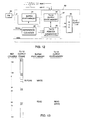
- 238000010586 diagram Methods 0.000 description 4
- XUIMIQQOPSSXEZ-UHFFFAOYSA-N Silicon Chemical compound [Si] XUIMIQQOPSSXEZ-UHFFFAOYSA-N 0.000 description 3
- 238000013507 mapping Methods 0.000 description 3
- 229910052710 silicon Inorganic materials 0.000 description 3
- 239000010703 silicon Substances 0.000 description 3
- ZAIPMKNFIOOWCQ-UEKVPHQBSA-N cephalexin Chemical compound C1([C@@H](N)C(=O)N[C@H]2[C@@H]3N(C2=O)C(=C(CS3)C)C(O)=O)=CC=CC=C1 ZAIPMKNFIOOWCQ-UEKVPHQBSA-N 0.000 description 2
- 238000010276 construction Methods 0.000 description 2
- 238000005516 engineering process Methods 0.000 description 2
- 239000000284 extract Substances 0.000 description 2
- 238000012546 transfer Methods 0.000 description 2
- 230000003247 decreasing effect Effects 0.000 description 1
- 230000001934 delay Effects 0.000 description 1
- 238000013461 design Methods 0.000 description 1
- 230000000694 effects Effects 0.000 description 1
- 239000011159 matrix material Substances 0.000 description 1
- 238000004148 unit process Methods 0.000 description 1
Images


Classifications
-
- H—ELECTRICITY
- H04—ELECTRIC COMMUNICATION TECHNIQUE
- H04J—MULTIPLEX COMMUNICATION
- H04J3/00—Time-division multiplex systems
- H04J3/02—Details
- H04J3/06—Synchronising arrangements
- H04J3/062—Synchronisation of signals having the same nominal but fluctuating bit rates, e.g. using buffers
- H04J3/0623—Synchronous multiplexing systems, e.g. synchronous digital hierarchy/synchronous optical network (SDH/SONET), synchronisation with a pointer process
-
- H—ELECTRICITY
- H04—ELECTRIC COMMUNICATION TECHNIQUE
- H04Q—SELECTING
- H04Q11/00—Selecting arrangements for multiplex systems
- H04Q11/04—Selecting arrangements for multiplex systems for time-division multiplexing
- H04Q11/0428—Integrated services digital network, i.e. systems for transmission of different types of digitised signals, e.g. speech, data, telecentral, television signals
- H04Q11/0478—Provisions for broadband connections
-
- H—ELECTRICITY
- H04—ELECTRIC COMMUNICATION TECHNIQUE
- H04J—MULTIPLEX COMMUNICATION
- H04J2203/00—Aspects of optical multiplex systems other than those covered by H04J14/05 and H04J14/07
- H04J2203/0001—Provisions for broadband connections in integrated services digital network using frames of the Optical Transport Network [OTN] or using synchronous transfer mode [STM], e.g. SONET, SDH
- H04J2203/0003—Switching fabrics, e.g. transport network, control network
- H04J2203/0012—Switching modules and their interconnections
-
- H—ELECTRICITY
- H04—ELECTRIC COMMUNICATION TECHNIQUE
- H04J—MULTIPLEX COMMUNICATION
- H04J2203/00—Aspects of optical multiplex systems other than those covered by H04J14/05 and H04J14/07
- H04J2203/0001—Provisions for broadband connections in integrated services digital network using frames of the Optical Transport Network [OTN] or using synchronous transfer mode [STM], e.g. SONET, SDH
- H04J2203/0089—Multiplexing, e.g. coding, scrambling, SONET
Definitions
- the invention relates to a method according to the preamble portion of the accompanying claim 1 and to an equipment according to the preamble portion of the accompanying claim 3 for elastic buffering in a synchronous digital telecommunication system.
- the current digital transmission network is plesiochronous, that is, e.g. each 2-Mbit/s basic multiplex system has a dedicated clock independent of any other system. It is therefore impossible to locate a single 2-Mbit/s signal in the bit stream of a higher-order system, but the higher-level signal has to be demultiplexed through each intermediate level down to the 2 Mbit/s level to extract the 2-Mbit/s signal. For this reason, especially the construction of branch connections requiring several multiplexers and demultiplexers has been expensive.
- Another disadvantage of the plesiochronous transmission network is that equipments from two different manufacturers are not usually compatible.
- the above drawbacks have led to the introduction of the new synchronous digital hierarchy SDH specified e.g. in the CCITT specifications G.707, G.708 and G.709.
- STM-N transfer frames Synchronous Transport Modules
- the bit rates are multiples of the bit rate of the lowest level.
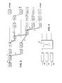
- Figure 1 illustrates the structure of the STM-N frame
- Figure 2 illustrates a single STM-1 frame
- the STM-N frame comprises a matrix with 9 rows and N x 270 columns so that there is one byte at the junction point between each row and the column.
- Rows 1-3 and rows 5-9 of the N x 9 first columns comprise a section overhead SOH, and the row 4 comprises an AU pointer.
- the rest of the frame structure is formed of a section having the length of N x 261 columns and containing the payload section of the STM-N frame.
- FIG. 2 illustrates a single STM-1 frame which is 270 bytes in length, as described above.
- the payload section comprises one or more administration units AU.
- the payload section consists of the administration unit AU-4, into which a virtual container VC-4 is inserted.
- the STM-1 transfer frame may contain several lower-level administration units (AU-3) each containing a corresponding lower-level virtual container (VC-3)).
- the VC-4 in turn consists of a path overhead POH located at the beginning of each row and having the length of one byte (9 bytes altogether), and of the payload section in which there are lower-level frames also comprising bytes allowing the interface justification to be performed in connection with mapping when the rate of the information signal to be mapped deviates from its nominal value to some extent. Mapping of the information signal into the STM-1 frame is described e.g. in the patent applications AU-B-34689/89 and FI-914746.
- Each byte in the AU-4 unit has its own location number.
- the above-mentioned AU pointer contains the location of the first byte of the VC-4 container in the AU-4 unit.
- the pointers allow positive or negative pointer justifications to be performed at different points in the SDH network. If a virtual container having a certain clock frequency is applied to a network node operating at a clock frequency lower than the above-mentioned clock frequency of the virtual container, the data buffer will be filled up. This requires negative justification: one byte is transferred from the received virtual container into the overhead section while the pointer value is decreased by one. If the rate of the received virtual container is lower than the clock rate of the node, the data buffer tends to be emptied, which calls for positive justification: a stuff byte is added to the received virtual container and the pointer value is incremented by one.
- Figure 3 shows how the STM-N frame can be formed of existing asynchronous bit streams.
- bit streams 1.5, 2, 6, 8, 34, 45 or 140 Mbit/s, shown in the right in the figure
- C containers C specified by CCITT.
- overhead bytes containing control data are inserted into the containers, thus obtaining the above-described virtual container VC-11, VC-12, VC-2, VC-3 or VC-4 (the first suffix in the abbreviations represents the level of hierarchy and the second suffix represents the bit rate).
- This virtual container remains intact while it passes through the synchronous network up to its point of delivery.
- the virtual containers are further formed either into tributary units TU or into AU units (AU-3 and AU-4) already mentioned above by providing them with pointers.
- the AU unit can be mapped directly into the STM-1 frame, whereas the TU units have to be assembled through tributary unit groups TUG and VC-3 and VC-4 units to form AU units which then can be mapped into the STM-1 frame.
- the mapping is indicated by a continuous thin line, the aligning with a broken line, and the multiplexing with a continuous thicker line.
- the STM-1 frame may be assembled in a number of alternative ways, and the content of the highest-level virtual container VC-4, for instance, may vary, depending on the level from which the assembly has been started and in which way the assembly has been performed.
- the STM-1 signal may thus contain e.g. 3 TU-3 units or 21 TU-2 units or 63 TU-12 units.
- the higher-level unit contains several lower-level units, e.g. the VC-4 unit contains TU-12 units (there are 63 such units in a single VC-4 unit, cf.
- the lower-level units are mapped into the higher-level frame by interleaving so that the first bytes are first taken consecutively from each one of the lower-level units, then the second bytes, etc.
- the VC-4 signal contains e.g. the above-mentioned 63 TU-12 signals
- these signals are located in the VC-4 frame as shown in Figure 2, i.e. the first byte of the first TU-12 signal is located first, then the first byte of the second TU-12 signal, etc.
- the second byte of the first TU-12 signal follows, etc.
- the TU-12 frame comprises four pointer bytes Vl-V4 so that the first quarter of the TU-12 frame contains the pointer byte V1, the second quarter contains the pointer byte V2, etc.
- the first two bytes V1 and V2 form the actual TU pointer value; the byte V3 is used for justification; and the byte V4 is reserved for other purposes.
- the TU-12 pointer which consists of the bytes V1 and V2, points to the first byte in the VC-12 unit. This first byte is indicated generally by the reference V5.
- the structure of the TU-12 frame appears more clearly from Figures 8 and 13, which will be referred to in more detail below.
- the above-described synchronization may take place in the synchronizing unit 42 of each incoming line, where the payload of the signal coming to the cross-connect equipment 41 is stored in an elastic buffer in synchronization with a clock signal extracted from the incoming signal and is read from the elastic buffer in synchronization with the clock signal of the cross-connect equipment.
- the control data contained in the higher-level frames such as pointers, have to be disassembled.
- the payload of a certain level of hierarchy thus has to pass through the elastic buffer in order that the synchronization with the sync of the cross-connection would be successful. If there are several channels of the same level of hierarchy, each one of them must have a dedicated independent elastic buffer. For instance, the above-described synchronization of the 63 VC-12 signals contained in a single STM-1 frame requires 63 elastic buffers independent of each other.
- the buffering is thus effected by constructing a single elastic buffer on a desired level of hierarchy. This buffer is then reproduced in a required number.
- a schematic block diagram illustrating this arrangement is shown in Figure 5, where the buffering of 63 VC-12 channels in the synchronizing unit 42 is used as an example similarly as above.
- a signal with the STM-1 frame structure is first applied to a common interpretation unit 51, which interprets the AU pointer data and the H4 byte in the path overhead (POH) of the VC-4 container so as to locate the TU-12 frames contained in the frame structure.
- the interpretation unit 51 then forwards the bytes of each TU-12 channel to a dedicated interpretation unit 52, of which there are thus 63 altogether in this specific case.
- the interpretation unit interprets the pointer of each TU-12 channel so as to determine the phase of the VC-12 signal contained therein. Due to the interleaving of the TU-12 units in the frame structure, each interpretation unit operates for only about 1/63 of the available time.
- Each VC-12 signal is stored in a dedicated elastic buffer 53 independent of any other buffer 53.
- the pointer data of each new TU-12 unit are generated in a dedicated generation unit 54, whereafter the final frame structure is assembled in a common generation unit 55 by combining the payloads from the elastic buffer memories with the new pointers and the new control data.
- the fill rate of each elastic buffer 53 is monitored by a dedicated monitoring unit 56.
- DE-C1-4018687 discloses a method for the transmission of an STM-1 frame structure comprising either four AU-31 or three AU-32 signals on the same level of hierarchy.
- the frame structure is reshaped to a frame comprising only one signal and one associated pointer in order to avoid the use of a dedicated buffer memory for each signal on each level of hierarchy.
- DE-A1-4018536 discloses a method and circuit arrangement for performing justifications in a synchronous transmission net.
- the circuit comprises a buffer memory divided into three parallel buffer memories, each submemory comprising a dedicated input. Justification is performed without changing the order of the bytes and without buffering the signals on a time-division basis.
- a problem with the above-described prior art buffering method is the high requirement of hardware. With the 63 TU-12 channels, for instance, it is thus practically impossible to place any other logical means in the microcircuit in addition to the 63 elastic buffers (due to restrictions imposed by present design methods and microcircuit technology). In the prior art arrangement, it is the memory means (such as D flip-flops, latches, etc.) that have the highest requirement of hardware. Modern microcircuit technology does allow the use of RAM memories integrated in a small space, but savings in the silicon area are obtained only in the construction of memory means having the size of 100 bits or more. The utilization of RAM memories provides only little advantage in the prior art arrangement, as the size of an individual elastic buffer is not necessarily above 100 bits.
- the object of the present invention is to avoid the above-described problems and to provide a method and an equipment which allow elastic buffering with less hardware than previously and which further allow RAM memory blocks to be used more advantageously than previously.
- a method for elastic buffering in a synchronous digital telecommunication system such as the SDH or SONET system, in which system the frame structure comprises a predetermined number of bytes of fixed length and a plurality of pointers, each of the pointers corresponding to a payload signal on the same level of hierarchy and each of said pointers indicating the phase of the corresponding payload signal within the frame structure, wherein pointer data is separated from payload signals contained in the frame structure and the payload signals are stored in at least one elastic buffer memory, characterized in that after the separation of the elastic buffering of the payloads of at least two signals of the same level of hierarchy is performed on a time-division basis in a buffer memory (101) common to said signals and having a data input to which said payload signals are applied in a sequential order defined by the frame structure, whereby each one of the signals is subjected to buffering over the same physical line in separate segments of time.
- a buffer memory (101) common to said signals and having a data input to which said payload signals are applied in
- the frame structure comprises a predetermined number of bytes of fixed length and a plurality of pointers, each of the pointers corresponding to a payload signal on the same level of hierarchy and each of said pointers indicating the phase of the corresponding payload signal within the frame structure
- the equipment comprising means for separating pointer data from payload signals contained in the frame structure, and memory means for storing payload signals contained in the frame structure, characterized in that said memory means is common to at least two payload signals of the same level of hierarchy, the equipment further comprising selection means connected to the memory means, the selection means selecting, on a time-division basis controlled by write and read counters, the payload signals to be written into the memory and to be read from the memory, respectively, whereby each one of the signals is subjected to writing over the same input line of the common memory in separate segments of time and each one of the signals is subjected to reading over the same output line of the common memory in
- the basic idea of the invention is to utilize time-divisioned architecture in buffering so that the elastic buffering of at least two signals of the same level of hierarchy is performed on a time-division basis in a buffer memory common to said signals.
- FIG. 6 shows a single time-division synchronizing unit applying the buffering principle according to the invention.
- the time-division principle is also applied to the frame disassembly and assembly and the monitoring of the fill rate of the buffer memory performed in the synchronizing unit 42, which are the subject-matter in separate parallel patent applications.
- the synchronizing unit 42 comprises sequentially arranged disassembly and assembly units 61 and 62 for TU-12 channels.
- An elastic buffer memory 63 common to all TU-12 channels is provided between the disassembly and assembly units, and the fill rate of the buffer memory is monitored by a common monitoring unit 64.
- the synchronizing unit 42 synchronizes an incoming AU-4 signal with another AU-4-level clock.
- the STM-1 signal is first applied to a common AU interpretation unit 51 which interprets AU-4 pointer data in a known manner (in compliance with the CCITT specifications, Ref. [1]), extracts the TU-12 signals from the AU-4 frame and applies the TU-12 signals to the disassembly unit 61 for further processing.
- the disassembly unit 61 interprets the TU-12 pointers and extracts VC-12 data from the TU-12 frame structure. Pointers are processed at one or more processing stages on a time-division basis, that is, the processing of at least two signals on the same level of hierarchy is performed over the same physical line.
- the disassembly unit 61 thus comprises a subprocessing unit 67 formed of at least one subprocessor 65 and a temporary memory 66.
- the subprocessing unit processes the pointers of the frame structure of at least two signals on the same level of hierarchy.
- all 63 TU-12 channels are buffered in the same buffer, but this is not necessary as several buffers may as well be positioned in parallel or in succession, provided that the elastic buffering of at least two TU-12 signals is performed on a time-division basis in a buffer memory common to said channels.
- the VC-12 payload coming to the TU disassembly unit 61 propagates through it unchanged, and is stored in the buffer memory 63 common to all TU-12 channels.
- the fill rate of the buffer memory 63 is monitored by the common monitoring unit 64.
- the reassembly of the TU-12 pointers and frames is performed in the assembly unit 62 at one or more processing stages on a time-division basis, that is, the signals of at least two channels are processed over the same physical line.
- the TU assembly unit 62 comprises a subprocessing unit 67 consisting of at least one subprocessor 65 and a temporary memory 66.
- the subprocessing unit 67 processes the pointers of the frame structure of at least two signals on the same level of hierarchy. In the present example all 63 channels are processed in the same assembly unit but this is not necessary as it is equally possible to position several assembly units in parallel or in succession.
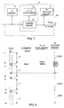
- FIG. 7 shows in more detail a single disassembly unit 61 comprising a V1 memory 71; a subprocessing unit formed of a TU-12 state memory 73 and a pointer read unit 72; and a V5 location memory 74.
- the disassembly unit will be described for a single frame of a single TU-12 signal while referring to Figure 8, in which there is a single TU-12 frame drawn in the left-hand side column; as is known per se the TU-12 frame comprises 140 data bytes (numbered beside the frame) and four pointer bytes V1 to V4.
- the length of one TU-12 frame is 500 ⁇ s so that it will be transmitted in four STM-1 frames in a basic case.
- the first byte of the TU-12 frame applied to the TU disassembly unit is first stored in the V1 memory 71.
- the data bytes coming after the V1 byte are stored in the buffer memory 63 as well as all other data bytes.
- the periods during which VC-12 data is stored in the buffer memory are indicated by the arrows A.
- the V1 byte is read from the memory and a new pointer word is generated for the pointer read unit 72 by combining the V1 and V2 bytes. A little before the generation of the new pointer word the old state of the pointer is read from the state memory 73 to the read unit.
- the old state comprises data on the values of the preceding (valid) pointer.
- the pointer read unit 72 processes the data received by it, as a result of which new state data is produced and stored in the state memory 73.
- a V5 flag (1 bit) is written concurrently in the V5 location memory 74 to an address determined by the new state.
- the location memory 74 comprises 63 x 140 memory locations having the length of one bit, that is, each channel has a memory location for each data byte of the TU-12 frame.
- the V5 flag that is, the logical one, is written to an address corresponding to the data byte to which the new pointer points.
- the other 139 memory locations contain the logical zero.
- the V5 location memory is read during the data bytes of the TU-12 frame, a value deviating from zero being obtained at a certain point (indicating the location of the V5 byte).
- Information about the location of the V5 byte (V5 loc. signal, Figure 7) is stored in the buffer memory.
- the incoming V1 and V2 bytes also indicate whether pointer justification mentioned above is required. With a negative justification, the content of the V3 byte is written in the buffer memory; with a positive justification, the data byte following the V3 byte is not written in the buffer memory.
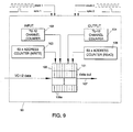
- FIG. 9 is a more detailed view of the elastic buffer 63 according to the invention, in which e.g. the VC-12 data is stored.
- the buffer comprises a buffer memory 101 itself and counter units controlling the buffer memory.
- the counter units include a first channel counter 102 and a first address counter unit 103; on the output side, there are a second channel counter 104 and a second address counter unit 105.
- the units on the input side control the writing of data into the memory while the units on the output side control the reading from the memory.
- the writing is synchronized by clock and synchronizing signals clockl and syncl, and on the output side by clock and synchronizing signals clock2 and sync2, which are independent of the corresponding signals on the input side.
- the buffer memory 101 comprises 63 memory units 106 (one for each channel), each comprising (in this specific case) 10 consecutive memory locations 106a having the width of 8 bits (i.e. the width of one byte). (In this specific case, a memory space of ten memory locations is reserved in each memory unit to allow for gaps in the SDH frame structures and various delays, among other things; the number of memory locations may be other than ten, e.g. sixteen).
- the address counter unit 103 comprises 63 address counters each one of which counts from one to ten, addressing a corresponding memory location in one memory unit. The phase of each address counter may be different as the fill rate of each channel in the buffer may vary.
- the first channel counter 102 counts continuously from one to sixty-three (1-63), and it is synchronized by the synchronizing signal syncl.
- the channel counter 102 selects one of the first address counters on a time-division basis, and a corresponding byte is written in the memory location 1 to 10 addressed by the selected address counter in the respective memory unit.
- the channel counter 104 selects one of the second address counters on a time-division basis, and the byte is read from the memory location addressed by the selected address counter to the output 107 of the buffer memory.
- FIGs 10 and 11 are more detailed views illustrating the monitoring of the fill rate of the elastic buffer, which according to the invention is performed by the common monitoring unit 64.
- the fill rate of each memory unit 106 i.e. that of each TU-12 channel
- the monitoring unit subtracts from the value of the read counter the value of the write counter and compares a resulting difference value E with predetermined limit values, which may be e.g. 2 and 8, as in Figure 11. In an ideal situation the difference value E is about 5 (a medium value).
- the monitoring of the fill rate is effected in synchronization with the output side (the read side).
- the address data obtained from the write counter 103 should be in phase with the address data from the read counter 105, i.e. the counters should correspond to the same channel (the channel to be selected on the write side is not the channel to which data is being written).
- the fill monitoring unit outputs data about the fill rate of each channel by using three different states indicated by 2 bits (full/empty/appropriate), and the data is applied to the TU assembly unit.
- Figures 12 and 13 illustrate the structure and operation of the TU assembly unit 62 of the synchronizing unit 42 similarly as the operation of the disassembly unit is illustrated in Figures 7 and 8.
- the assembly unit 62 generates the above-described V bytes and decides whether justification is required.
- the only variable on the frame structure assembly side is the TU-12 pointer.
- the above-described V5 byte may be at any location in the TU-12 frame, and this location has to be indicated by the V1 and V2 bytes (the time instant of the V5 flag obtained from the buffer memory has to be converted into a pointer number).
- the clock and synchronizing signals clock2 and sync2 for the assembly side ( Figure 9) are independent of the respective signals of the disassembly unit, whereas they are equal to those used on the read side of the buffering.
- a reference counter 92 and a buffer state memory 91 connected to it are provided at the input of the assembly unit.
- the buffer state memory 91 in turn is connected to a TU-12 pointer generator 93 which constitutes its own subprocessing unit 67 together with the state memory 94 of the output.
- the output of the state memory is connected to a multiplexer 95 having another input to which data bytes from the buffer memory 63 are connected directly.
- the reference counter 92 counts the bytes 0 to 139 of the VC-12 frame ( Figure 10, the left-hand side column).
- the V5 location data signal (V5 loc.) is applied to the input of the assembly unit. This signal corresponds to the signal generated in the disassembly unit.
- the current value of the reference counter is stored in the state memory 91 of the buffer.
- the TU-12 pointer generator 93 performs the processing. For the processing the value of the reference counter from the state memory 91 of the buffer, and the old state data of the TU-12 pointer from the state memory 94 of the output are read into the pointer generator.
- the processing produces new pointer state data containing e.g. the values of the V1 and V2 bytes.
- the new state data is stored in place of the old data in the state memory of the output.
- the state data of the pointer and the data from the buffer memory are combined in the multiplexer 95, which outputs the reassembled TU-12 channels.
- Pointer justification is performed in the assembly unit by applying data on the fill rate of the buffer from the monitor 64 to the TU-12 pointer generator 93.
- the data indicating one of the three possible states (full, empty, appropriate, as described above) is represented by two bits.
- the pointer generator 93 interprets the fill rate so as to decide whether justification is required.
- the signal obtained at the output of the TU assembly unit is applied to the AU generation unit 55 ( Figures 5 and 6), where the final AU-4 signal is generated in a manner known per se.
- frames such as VC-11, VC-21, VC-22, VC-31, VC-32, VC-3 and VC-4 can be buffered in the SDH system; and frames such as VC-1.5, VC-2, VC-3, VC-4, or VC-6 can be buffered in the SONET system.
- the frame disassembly and assembly and the monitoring of the fill rate of the buffer memory need not necessarily be time-divisional, as above, although it is advantageous to effect them as described above.
- the common unit performing the buffering of the channels according to the invention may also form part of a larger buffering unit irrespective of the way in which the data to be buffered is applied to the input of the larger unit or the way in which the buffered data is applied to the output of the larger unit.
Landscapes
- Engineering & Computer Science (AREA)
- Computer Networks & Wireless Communication (AREA)
- Computer Hardware Design (AREA)
- Signal Processing (AREA)
- Time-Division Multiplex Systems (AREA)
- Financial Or Insurance-Related Operations Such As Payment And Settlement (AREA)
- Mobile Radio Communication Systems (AREA)
Claims (4)
- Verfahren zur elastischen Pufferung in einem synchronen digitalen Fernmeldesystem, wie beispielsweise das SDH- oder SONET-System, wobei in dem System die Rahmenstruktur eine vorbestimmte Zahl von Bytes mit fester Länge und eine Vielzahl von Zeigern aufweist, wobei jeder der Zeiger einem Nutzlastsignal auf derselben Hierarchieebene entspricht und jeder der Zeiger die Phase des entsprechenden Nutzlastsignals innerhalb der Rahmenstruktur anzeigt, wobei Zeigerdaten von in der Rahmenstruktur enthaltenen Nutzlastsignalen getrennt und die Nutzlastsignale in zumindest einem elastischen Pufferspeicher gespeichert werden,
dadurch gekennzeichnet, daß
nach der Trennung die elastische Pufferung der Nutzlasten zumindest zweier Signale auf derselben Hierarchieebene auf einer Zeitmultiplexbasis in einem den Signalen gemeinsamen Pufferspeicher (101) durchgeführt wird, der einen Dateneingang aufweist, dem die Nutzlastsignale in einer durch die Rahmenstruktur definierten sequentiellen Reihenfolge zugeführt werden, wodurch jedes der Signale der Pufferung über derselben physikalischen Leitung in getrennten Zeitsegmenten unterzogen wird. - Verfahren nach Anspruch 1,
dadurch gekennzeichnet, daß
die elastische Pufferung der Nutzlasten aller Signale auf derselben Hierarchieebene auf einer Zeitmultiplexbasis in dem gemeinsamen Pufferspeicher (101) durchgeführt wird. - Einrichtung zum Realisieren des Verfahrens nach Patentanspruch 1 zur elastischen Pufferung in einem synchronen digitalen Fernmeldesystem, bei dem die Rahmenstruktur eine vorbestimmte Zahl von Bytes mit fester Länge und eine Vielzahl von Zeigern umfaßt, wobei jeder der Zeiger einem Nutzlastsignal auf derselben Hierarchieebene entspricht und jeder der Zeiger die Phase des entsprechenden Nutzlastsignals innerhalb der Rahmenstruktur anzeigt, wobei die Einrichtung umfaßtdadurch gekennzeichnet, daßeine Einrichtung (71, 72) zum Trennen der Zeigerdaten von den in der Rahmenstruktur enthaltenen Nutzlastsignalen, undeine Speichereinrichtung (101) zum Speichern der in der Rahmenstruktur enthaltenen Nutzlastsignale,
die Speichereinrichtung (101) von zumindest zwei Nutzlastsignalen auf derselben Hierarchieebene gemeinsam genutzt wird, wobei die Einrichtung des weiteren umfaßt eine Auswahleinrichtung (102, 104), die mit der Speichereinrichtung (101) verbunden ist, wobei die Auswahleinrichtung (102, 104) auf einer durch Schreib- und Lesezähler (103, 105) gesteuerten Zeitmultiplexbasis die in den Speicher zu schreibenden bzw. aus dem Speicher zu lesenden Nutzlastsignale auswählt, wobei jedes der Signale einem Schreiben über dieselbe Eingangsleitung des gemeinsamen Speichers in getrennten Zeitsegmenten unterzogen wird und jedes der Signale einem Lesen über dieselbe Ausgangsleitung des gemeinsamen Speichers in getrennten Zeitsegmenten unterzogen wird. - Einrichtung nach Anspruch 3,
dadurch gekennzeichnet, daß
die Auswahleinrichtung Kanalzähler (102, 104) aufweist mit einem alle Nutzlastsignale auf derselben Hierarchieebene enthaltenden Zählzyklus.
Applications Claiming Priority (3)
| Application Number | Priority Date | Filing Date | Title |
|---|---|---|---|
| FI922569 | 1992-06-03 | ||
| FI922569A FI90486C (fi) | 1992-06-03 | 1992-06-03 | Menetelmä ja laite synkronisessa digitaalisessa tietoliikennejärjestelmässä suoritettavan elastisen puskuroinnin toteuttamiseksi |
| PCT/FI1993/000236 WO1993025029A1 (en) | 1992-06-03 | 1993-06-01 | Method and equipment for elastic buffering in a synchronous digital telecommunication system |
Publications (2)
| Publication Number | Publication Date |
|---|---|
| EP0788694A1 EP0788694A1 (de) | 1997-08-13 |
| EP0788694B1 true EP0788694B1 (de) | 1999-12-22 |
Family
ID=8535415
Family Applications (1)
| Application Number | Title | Priority Date | Filing Date |
|---|---|---|---|
| EP93910065A Expired - Lifetime EP0788694B1 (de) | 1992-06-03 | 1993-06-01 | Verfahren und einrichtung zur elastischen pufferung in einem synchronen digitalen fernmeldesystem |
Country Status (9)
| Country | Link |
|---|---|
| US (1) | US5687318A (de) |
| EP (1) | EP0788694B1 (de) |
| JP (1) | JP3429307B2 (de) |
| AU (1) | AU671453B2 (de) |
| DE (1) | DE69327412T2 (de) |
| DK (1) | DK0788694T3 (de) |
| FI (1) | FI90486C (de) |
| NZ (1) | NZ252188A (de) |
| WO (1) | WO1993025029A1 (de) |
Families Citing this family (15)
| Publication number | Priority date | Publication date | Assignee | Title |
|---|---|---|---|---|
| US5885489A (en) * | 1992-11-03 | 1999-03-23 | Eta Process Plant Limited | Packing elements |
| IT1264582B1 (it) * | 1993-06-11 | 1996-10-04 | Alcatel Italia | Metodo e circuiti per la realizzazione e la programmazione delle funzioni di connessione in un apparato sincrono |
| JP3271444B2 (ja) | 1994-11-11 | 2002-04-02 | 富士通株式会社 | Bip−2演算回路およびbip−2チェック回路 |
| GB9509216D0 (en) * | 1995-05-05 | 1995-06-28 | Plessey Telecomm | Retiming arrangement for SDH data transmission system |
| DE19542230C2 (de) * | 1995-11-13 | 1998-08-27 | Siemens Ag | Verfahren zur Auswahl von verketteten Signalen aus Empfangssignalen der Synchron-Digital-Hierarchie |
| GB2312353B (en) * | 1996-04-16 | 2000-12-06 | Gpt Ltd | Digital telecommunications transmision systems |
| DE19640547B4 (de) * | 1996-10-01 | 2005-11-03 | Marconi Communications Gmbh | Verfahren und Einrichtung zur Durchschaltung von digitalen Signalen |
| JP3425046B2 (ja) * | 1996-11-29 | 2003-07-07 | 富士通株式会社 | 受信ポインタ処理装置 |
| US6625653B1 (en) * | 2000-06-08 | 2003-09-23 | Eci Telecom Ltd. | Network protection architecture |
| US20020027929A1 (en) * | 2000-06-15 | 2002-03-07 | John Eaves | System and method for mapping signals to a data structure having a fixed frame size |
| KR100399413B1 (ko) * | 2001-08-06 | 2003-09-26 | 삼성전자주식회사 | 동기식 디지털 계위 전송 시스템의 고계위 신호 연결 장치 |
| JP3818884B2 (ja) * | 2001-09-19 | 2006-09-06 | 富士通株式会社 | 伝送装置 |
| US7353288B1 (en) * | 2001-10-17 | 2008-04-01 | Ciena Corporation | SONET/SDH payload re-mapping and cross-connect |
| DE102010045518A1 (de) | 2010-09-15 | 2012-03-15 | Volkswagen Aktiengesellschaft | Verfahren und Vorrichtung zum Betrieb einer elektromechanischen Lenkung |
| DE102012014305A1 (de) | 2012-07-19 | 2014-01-23 | Volkswagen Aktiengesellschaft | Fahrzeuglenksystem mit einer Energieanpassung an Fahrzeugbordnetz |
Family Cites Families (10)
| Publication number | Priority date | Publication date | Assignee | Title |
|---|---|---|---|---|
| CA1326719C (en) * | 1989-05-30 | 1994-02-01 | Telecommunications Research Laboratories | Ds3 to 28 vt1.5 sonet interface circuit |
| DE4018687A1 (de) * | 1989-07-18 | 1991-01-31 | Siemens Ag | Verfahren und anordnung zur uebertragung eines blocks aus vier verwaltungseinheiten au-31 oder aus drei verwaltungseinheiten au-32 in einem synchronen transport-modul stm-1 |
| DE3934248A1 (de) * | 1989-10-13 | 1991-04-18 | Standard Elektrik Lorenz Ag | Multiplexer und demultiplexer, insbesondere fuer nachrichtenuebertragungs-netze mit einer synchronen hierarchie der digitalsignale |
| LU87714A1 (de) * | 1989-11-29 | 1990-07-24 | Siemens Ag | Verfahren zum uebertragen eines digitalen breitbandsignals in einer untersystemeinheitenkette ueber ein netz einer synchron-digital-multiplexhierarchie |
| FR2656479B1 (de) * | 1989-12-27 | 1994-04-08 | Alcatel Cit | |
| ES2146576T3 (es) * | 1990-03-14 | 2000-08-16 | Cit Alcatel | Disposicion de bucle con enganche de pase. |
| US5111485A (en) * | 1990-05-18 | 1992-05-05 | Northern Telecom Limited | Method of and circuit for synchronizing data |
| DE4018536A1 (de) | 1990-06-09 | 1991-12-19 | Ant Nachrichtentech | Verfahren und schaltungsanordnung zur taktanpassung |
| JP2599819B2 (ja) * | 1990-11-02 | 1997-04-16 | 富士通株式会社 | データリンク終端方式 |
| US5390180A (en) * | 1991-10-10 | 1995-02-14 | Nec America, Inc. | SONET DS-N desynchronizer |
-
1992
- 1992-06-03 FI FI922569A patent/FI90486C/fi active
-
1993
- 1993-06-01 JP JP50024394A patent/JP3429307B2/ja not_active Expired - Fee Related
- 1993-06-01 WO PCT/FI1993/000236 patent/WO1993025029A1/en not_active Ceased
- 1993-06-01 US US08/360,776 patent/US5687318A/en not_active Expired - Lifetime
- 1993-06-01 DK DK93910065T patent/DK0788694T3/da active
- 1993-06-01 AU AU40726/93A patent/AU671453B2/en not_active Ceased
- 1993-06-01 DE DE69327412T patent/DE69327412T2/de not_active Expired - Lifetime
- 1993-06-01 NZ NZ252188A patent/NZ252188A/en not_active IP Right Cessation
- 1993-06-01 EP EP93910065A patent/EP0788694B1/de not_active Expired - Lifetime
Also Published As
| Publication number | Publication date |
|---|---|
| FI90486C (fi) | 1999-08-11 |
| HK1002378A1 (en) | 1998-08-21 |
| DK0788694T3 (da) | 2000-05-08 |
| JPH07507424A (ja) | 1995-08-10 |
| DE69327412D1 (de) | 2000-01-27 |
| AU671453B2 (en) | 1996-08-29 |
| DE69327412T2 (de) | 2000-05-18 |
| US5687318A (en) | 1997-11-11 |
| FI922569A0 (fi) | 1992-06-03 |
| EP0788694A1 (de) | 1997-08-13 |
| JP3429307B2 (ja) | 2003-07-22 |
| FI90486B (fi) | 1993-10-29 |
| WO1993025029A1 (en) | 1993-12-09 |
| AU4072693A (en) | 1993-12-30 |
| NZ252188A (en) | 1995-12-21 |
Similar Documents
| Publication | Publication Date | Title |
|---|---|---|
| EP0788695B1 (de) | Verfahren zum zerlegen und zusammensetzen von rahmenstrukturen mit zeigern | |
| EP0788694B1 (de) | Verfahren und einrichtung zur elastischen pufferung in einem synchronen digitalen fernmeldesystem | |
| US5570358A (en) | Method for Implementing switching in time or space domain | |
| EP0645065B1 (de) | Verfahren und einrichtung zur überwachung der füllrate eines elastischen pufferspeichers in einem synchronen digitalen fernmeldesystem | |
| EP0699363B1 (de) | Verfahren und vorrichtung zum bestimmen einer stopfentscheidung in einem knoten eines synchronen digitalen nachrichtenübertragungssystems (sdh) | |
| US5535203A (en) | Method for implementing time switching, and a time switch | |
| WO1994003022A1 (en) | Method for implementing time switching and a time switch | |
| HK1002378B (en) | Method and equipment for elastic buffering in a synchronous digital telecommunication system | |
| HK1011805B (en) | Method and equipment for monitoring the fill rate of an elastic buffer memory in a synchronous digital telecommunication system | |
| HK1002380B (en) | Method for disassembling and assembling frame structures containing pointers | |
| HK1011820B (en) | Method for implementing switching in time or space domain | |
| HK1011821B (en) | Method for implementing time switching and a time switch |
Legal Events
| Date | Code | Title | Description |
|---|---|---|---|
| PUAI | Public reference made under article 153(3) epc to a published international application that has entered the european phase |
Free format text: ORIGINAL CODE: 0009012 |
|
| 17P | Request for examination filed |
Effective date: 19941219 |
|
| AK | Designated contracting states |
Kind code of ref document: A1 Designated state(s): BE CH DE DK FR GB IT LI NL PT SE |
|
| RAP1 | Party data changed (applicant data changed or rights of an application transferred) |
Owner name: NOKIA TELECOMMUNICATIONS OY |
|
| 17Q | First examination report despatched |
Effective date: 19980205 |
|
| GRAG | Despatch of communication of intention to grant |
Free format text: ORIGINAL CODE: EPIDOS AGRA |
|
| GRAG | Despatch of communication of intention to grant |
Free format text: ORIGINAL CODE: EPIDOS AGRA |
|
| GRAH | Despatch of communication of intention to grant a patent |
Free format text: ORIGINAL CODE: EPIDOS IGRA |
|
| GRAH | Despatch of communication of intention to grant a patent |
Free format text: ORIGINAL CODE: EPIDOS IGRA |
|
| GRAA | (expected) grant |
Free format text: ORIGINAL CODE: 0009210 |
|
| AK | Designated contracting states |
Kind code of ref document: B1 Designated state(s): BE CH DE DK FR GB IT LI NL PT SE |
|
| RAP2 | Party data changed (patent owner data changed or rights of a patent transferred) |
Owner name: NOKIA NETWORKS OY |
|
| REG | Reference to a national code |
Ref country code: CH Ref legal event code: EP |
|
| ITF | It: translation for a ep patent filed | ||
| REG | Reference to a national code |
Ref country code: CH Ref legal event code: NV Representative=s name: ICB INGENIEURS CONSEILS EN BREVETS SA |
|
| REF | Corresponds to: |
Ref document number: 69327412 Country of ref document: DE Date of ref document: 20000127 |
|
| ET | Fr: translation filed | ||
| NLT2 | Nl: modifications (of names), taken from the european patent patent bulletin |
Owner name: NOKIA NETWORKS OY |
|
| REG | Reference to a national code |
Ref country code: PT Ref legal event code: SC4A Free format text: AVAILABILITY OF NATIONAL TRANSLATION Effective date: 19991223 |
|
| REG | Reference to a national code |
Ref country code: DK Ref legal event code: T3 |
|
| PLBE | No opposition filed within time limit |
Free format text: ORIGINAL CODE: 0009261 |
|
| STAA | Information on the status of an ep patent application or granted ep patent |
Free format text: STATUS: NO OPPOSITION FILED WITHIN TIME LIMIT |
|
| 26N | No opposition filed | ||
| REG | Reference to a national code |
Ref country code: GB Ref legal event code: IF02 |
|
| REG | Reference to a national code |
Ref country code: GB Ref legal event code: 732E |
|
| PGFP | Annual fee paid to national office [announced via postgrant information from national office to epo] |
Ref country code: CH Payment date: 20070530 Year of fee payment: 15 |
|
| PGFP | Annual fee paid to national office [announced via postgrant information from national office to epo] |
Ref country code: PT Payment date: 20070531 Year of fee payment: 15 |
|
| PGFP | Annual fee paid to national office [announced via postgrant information from national office to epo] |
Ref country code: NL Payment date: 20070603 Year of fee payment: 15 |
|
| PGFP | Annual fee paid to national office [announced via postgrant information from national office to epo] |
Ref country code: SE Payment date: 20070607 Year of fee payment: 15 |
|
| PGFP | Annual fee paid to national office [announced via postgrant information from national office to epo] |
Ref country code: DK Payment date: 20070618 Year of fee payment: 15 |
|
| PGFP | Annual fee paid to national office [announced via postgrant information from national office to epo] |
Ref country code: IT Payment date: 20070625 Year of fee payment: 15 |
|
| PGFP | Annual fee paid to national office [announced via postgrant information from national office to epo] |
Ref country code: BE Payment date: 20070821 Year of fee payment: 15 |
|
| REG | Reference to a national code |
Ref country code: GB Ref legal event code: 732E |
|
| REG | Reference to a national code |
Ref country code: FR Ref legal event code: TP Ref country code: FR Ref legal event code: CD |
|
| REG | Reference to a national code |
Ref country code: PT Ref legal event code: MM4A Free format text: LAPSE DUE TO NON-PAYMENT OF FEES Effective date: 20081202 |
|
| BERE | Be: lapsed |
Owner name: SCHOFIELD TECHNOLOGIES LLC Effective date: 20080630 |
|
| PG25 | Lapsed in a contracting state [announced via postgrant information from national office to epo] |
Ref country code: PT Free format text: LAPSE BECAUSE OF NON-PAYMENT OF DUE FEES Effective date: 20081202 |
|
| REG | Reference to a national code |
Ref country code: CH Ref legal event code: PL |
|
| REG | Reference to a national code |
Ref country code: DK Ref legal event code: EBP |
|
| EUG | Se: european patent has lapsed | ||
| NLV4 | Nl: lapsed or anulled due to non-payment of the annual fee |
Effective date: 20090101 |
|
| PG25 | Lapsed in a contracting state [announced via postgrant information from national office to epo] |
Ref country code: BE Free format text: LAPSE BECAUSE OF NON-PAYMENT OF DUE FEES Effective date: 20080630 |
|
| PG25 | Lapsed in a contracting state [announced via postgrant information from national office to epo] |
Ref country code: NL Free format text: LAPSE BECAUSE OF NON-PAYMENT OF DUE FEES Effective date: 20090101 |
|
| PG25 | Lapsed in a contracting state [announced via postgrant information from national office to epo] |
Ref country code: LI Free format text: LAPSE BECAUSE OF NON-PAYMENT OF DUE FEES Effective date: 20080630 Ref country code: CH Free format text: LAPSE BECAUSE OF NON-PAYMENT OF DUE FEES Effective date: 20080630 |
|
| PG25 | Lapsed in a contracting state [announced via postgrant information from national office to epo] |
Ref country code: IT Free format text: LAPSE BECAUSE OF NON-PAYMENT OF DUE FEES Effective date: 20080601 |
|
| PG25 | Lapsed in a contracting state [announced via postgrant information from national office to epo] |
Ref country code: DK Free format text: LAPSE BECAUSE OF NON-PAYMENT OF DUE FEES Effective date: 20090106 |
|
| PG25 | Lapsed in a contracting state [announced via postgrant information from national office to epo] |
Ref country code: DK Free format text: LAPSE BECAUSE OF NON-PAYMENT OF DUE FEES Effective date: 20080630 |
|
| PG25 | Lapsed in a contracting state [announced via postgrant information from national office to epo] |
Ref country code: SE Free format text: LAPSE BECAUSE OF NON-PAYMENT OF DUE FEES Effective date: 20080602 |
|
| PGFP | Annual fee paid to national office [announced via postgrant information from national office to epo] |
Ref country code: GB Payment date: 20120525 Year of fee payment: 20 Ref country code: FR Payment date: 20120614 Year of fee payment: 20 |
|
| PGFP | Annual fee paid to national office [announced via postgrant information from national office to epo] |
Ref country code: DE Payment date: 20120629 Year of fee payment: 20 |
|
| REG | Reference to a national code |
Ref country code: DE Ref legal event code: R071 Ref document number: 69327412 Country of ref document: DE |
|
| REG | Reference to a national code |
Ref country code: GB Ref legal event code: PE20 Expiry date: 20130531 |
|
| PG25 | Lapsed in a contracting state [announced via postgrant information from national office to epo] |
Ref country code: DE Free format text: LAPSE BECAUSE OF EXPIRATION OF PROTECTION Effective date: 20130604 Ref country code: GB Free format text: LAPSE BECAUSE OF EXPIRATION OF PROTECTION Effective date: 20130531 |