EP0786801A1 - Procédé de transfert d'une couche mince d'un substrat initial sur un substrat final - Google Patents
Procédé de transfert d'une couche mince d'un substrat initial sur un substrat final Download PDFInfo
- Publication number
- EP0786801A1 EP0786801A1 EP97400151A EP97400151A EP0786801A1 EP 0786801 A1 EP0786801 A1 EP 0786801A1 EP 97400151 A EP97400151 A EP 97400151A EP 97400151 A EP97400151 A EP 97400151A EP 0786801 A1 EP0786801 A1 EP 0786801A1
- Authority
- EP
- European Patent Office
- Prior art keywords
- substrate
- thin layer
- face
- layer
- initial
- Prior art date
- Legal status (The legal status is an assumption and is not a legal conclusion. Google has not performed a legal analysis and makes no representation as to the accuracy of the status listed.)
- Granted
Links
Images

Classifications
-
- H—ELECTRICITY
- H10—SEMICONDUCTOR DEVICES; ELECTRIC SOLID-STATE DEVICES NOT OTHERWISE PROVIDED FOR
- H10P—GENERIC PROCESSES OR APPARATUS FOR THE MANUFACTURE OR TREATMENT OF DEVICES COVERED BY CLASS H10
- H10P90/00—Preparation of wafers not covered by a single main group of this subclass, e.g. wafer reinforcement
- H10P90/19—Preparing inhomogeneous wafers
- H10P90/1904—Preparing vertically inhomogeneous wafers
- H10P90/1906—Preparing SOI wafers
- H10P90/1914—Preparing SOI wafers using bonding
- H10P90/1916—Preparing SOI wafers using bonding with separation or delamination along an ion implanted layer, e.g. Smart-cut
-
- H—ELECTRICITY
- H10—SEMICONDUCTOR DEVICES; ELECTRIC SOLID-STATE DEVICES NOT OTHERWISE PROVIDED FOR
- H10W—GENERIC PACKAGES, INTERCONNECTIONS, CONNECTORS OR OTHER CONSTRUCTIONAL DETAILS OF DEVICES COVERED BY CLASS H10
- H10W10/00—Isolation regions in semiconductor bodies between components of integrated devices
- H10W10/10—Isolation regions comprising dielectric materials
- H10W10/181—Semiconductor-on-insulator [SOI] isolation regions, e.g. buried oxide regions of SOI wafers
-
- H—ELECTRICITY
- H10—SEMICONDUCTOR DEVICES; ELECTRIC SOLID-STATE DEVICES NOT OTHERWISE PROVIDED FOR
- H10P—GENERIC PROCESSES OR APPARATUS FOR THE MANUFACTURE OR TREATMENT OF DEVICES COVERED BY CLASS H10
- H10P72/00—Handling or holding of wafers, substrates or devices during manufacture or treatment thereof
- H10P72/70—Handling or holding of wafers, substrates or devices during manufacture or treatment thereof for supporting or gripping
- H10P72/74—Handling or holding of wafers, substrates or devices during manufacture or treatment thereof for supporting or gripping using temporarily an auxiliary support
- H10P72/7434—Handling or holding of wafers, substrates or devices during manufacture or treatment thereof for supporting or gripping using temporarily an auxiliary support used in a transfer process involving at least two transfer steps, i.e. including an intermediate handle substrate
-
- Y—GENERAL TAGGING OF NEW TECHNOLOGICAL DEVELOPMENTS; GENERAL TAGGING OF CROSS-SECTIONAL TECHNOLOGIES SPANNING OVER SEVERAL SECTIONS OF THE IPC; TECHNICAL SUBJECTS COVERED BY FORMER USPC CROSS-REFERENCE ART COLLECTIONS [XRACs] AND DIGESTS
- Y10—TECHNICAL SUBJECTS COVERED BY FORMER USPC
- Y10S—TECHNICAL SUBJECTS COVERED BY FORMER USPC CROSS-REFERENCE ART COLLECTIONS [XRACs] AND DIGESTS
- Y10S438/00—Semiconductor device manufacturing: process
- Y10S438/977—Thinning or removal of substrate
Definitions
- the present invention relates to a method of transferring a thin layer from an initial substrate to a final substrate.
- thin layer is meant a layer whose thickness is of the order of a few micrometers and whose diameter, or other dimension, can reach 100 mm or more.
- Thin film transfer finds applications in particular in the production of microelectronics devices.
- the method can be used, for example, to transfer thin layers of monocrystalline semiconductor, comprising electronic circuits, onto a glass plate such as a plate of a flat display screen with active matrix.
- Another application of thin film transfer can be the fabrication of three-dimensional structures of integrated circuits.
- a thin layer within the meaning of the present invention cannot, because of its dimensions and its too great brittleness, be transported as it is.
- a transfer substrate which has a thickness of several hundred microns.
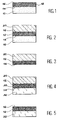
- Figures 1 to 5 illustrate a known method of transferring a thin layer from an initial substrate to a final substrate without inversion of the thin layer.
- FIG. 1 shows the initial substrate 10 and the thin layer 12.
- the thin layer in which one has manufactured, for example electronic circuits, is integral with the substrate 10 by a first face 14.
- a handle substrate 20 is bonded to the second face 16 of the thin layer in order to obtain the structure of FIG. 2.
- FIGS. 3 and 4 show successively the elimination of the initial substrate 10 and the bonding of the first face of the thin layer 12 to one face 30 of a final substrate 32.
- the initial substrate is removed, for example, by mechanical abrasion.
- a last step of the known method represented in FIG. 5, consists in eliminating the handle substrate.
- the handle substrate is completely destroyed by mechanical abrasion or by chemical attack. It can also be eliminated by combining these two means.
- the structure of FIG. 5 is obtained with the final substrate 32 and the thin layer 12.
- the handle substrate is destroyed during its elimination. It cannot therefore be reused for another transfer operation.
- An object of the present invention is to provide a method of transfer without reversing a thin layer, using a handle substrate in which the handle substrate is not destroyed, but can be reused.
- Another object of the present invention is to provide a method for transferring a thin layer in which the thin layer does not undergo significant stress when removing the handle support.
- the thin layer may contain active elements.
- this layer is made of semiconductor material and the active elements are produced before the step of joining with the handle substrate.
- Cleavage thus eliminates the massive part of the handle substrate. Only the surface layer of the handle substrate remains on the second face of the thin layer. This very thin surface layer can, in certain cases, be left in place on the thin layer. It can then play the role of a passivation layer of the thin layer, for example.
- the thin layer does not undergo significant stress.
- it does not undergo the constraints of a mechanical abrasion treatment.
- the joining between the thin layer and the handle substrate, as well as the joining of the thin layer on the final substrate can be carried out either by an adhesive bonding using an adhesive, or by a direct bonding, that is to say without adhesive compound.
- the elimination of the initial substrate can be done by detaching this substrate from the thin layer or by destroying the substrate.
- FIGS. 6A, 6B and 7 to 10 identical or similar to elements of FIGS. 1 to 5, bear, in the following description, identical references to which the value 100 has been added.
- the handle substrate 120 used in the method of the invention has a solid part 122 and a surface layer 124.
- the solid part and the surface layer are separated by a cleavage zone 126.
- the cleavage zone is obtained, for example, by implantation through a face 128 of the substrate 120 of hydrogen ions H + at a dose greater than 3.10 16 cm -2 and an energy less than 50 keV. These implanted ions form, at the average depth of penetration of the ions, a layer of gaseous microbubbles which defines the cleavage zone 126.
- the cleavage zone is located at a depth of the order of 0.5 ⁇ m from the face 128 of the substrate. This therefore corresponds to the thickness of the surface layer 124.
- FIG. 6B shows the initial substrate 110 and the thin layer. It is similar to Figure 1 already described.
- the thin layer has a first face 114 secured to the substrate and a second face 116, which is free.
- the structure formed of the initial substrate 110 and of the thin layer can be a SOI (silicon on insulator) type structure. It then comprises a thin layer of silicon possibly containing integrated circuits and forming said thin layer, a layer of silicon oxide which can be considered as also forming part of the thin layer, and a massive part of silicon which constitutes the initial substrate.
- SOI silicon on insulator
- FIG. 7 illustrates the step of joining the handle substrate 120 to the structure comprising the initial substrate 110 and the thin layer 112.
- the surface layer 124 of the substrate 120 is bonded to the face 116 of the thin layer.
- the bonding can be adhesive, that is to say bonding by means of an adhesive of a type resistant to high temperatures.
- Bonding can also be direct.
- the faces 116 and 128 are prepared by mechanochemical polishing and / or chemical cleaning.
- the surfaces thus prepared are brought into contact and the structure obtained is annealed under a nitrogen atmosphere.
- the annealing temperature is chosen so as to obtain good mechanical strength of the assembly formed by the handle substrate and the thin layer. However, it is chosen to be low enough not to degrade any integrated circuits formed in the thin layer. For example, if the thin layer contains conductive aluminum parts, the annealing temperature should not exceed 450 ° C.
- the annealing temperature should be chosen in such a way that it does not cause premature cleavage of the handle substrate 120.
- the annealing is carried out at a temperature of the order of 350 °. vs.
- a next step in the process is the removal of the initial substrate. It is illustrated in Figure 8.
- the initial substrate can be detached by tearing off.
- opposite tensile forces are exerted on the initial substrate and the handle substrate. able to cause tearing of the initial substrate along the first face of the thin layer.
- a layer of sacrificial material can be provided in the initial substrate.
- This layer is preferably provided on the face of the initial substrate in contact with the first face 114 of the thin layer, that is to say at the interface between the initial substrate and the thin layer.
- the initial substrate can also be totally destroyed by mechanical abrasion, by chemical attack or even by a combination of these two means.
- the initial substrate is of the silicon on insulator type
- its elimination involves mechanical abrasion, that is to say running in or rectification of the massive part of silicon.
- TMAH Tetra Methyl Ammonium Hydroxide
- the silicon oxide layer of the SOI structure serves as an etching stop layer.
- FIG. 9 shows the structure obtained after the first face 114 of the thin layer has been joined to the surface face 134 of the final substrate 132.
- the final substrate 132 is for example a glass plate.
- the attachment of the handle substrate to the thin layer it is possible for the attachment to the final substrate of make either an adhesive bonding with glue or a direct bonding.
- Direct bonding involves preparing the faces 114 and 134 by mechanochemical polishing and / or chemical cleaning, bringing these surfaces into contact and, optionally annealing the structure thus obtained under nitrogen atmosphere.
- Annealing carried out at a temperature of the order of 350 ° C., improves the adhesion.
- a next step in the process of the invention is the elimination of the handle substrate which is carried out by cleavage in the cleavage zone 126 (see FIG. 6A).
- the cleavage of the handle substrate is caused by heat treatment.
- This heat treatment causes a crystalline rearrangement effect in the handle substrate and a pressure effect in the layer of gas microbubbles to separate the solid part from the surface layer.
- the structure shown in FIG. 10 is thus obtained in which only the surface layer 124 of the handle substrate remains on the face 116 of the thin layer.
- the heat treatment may be common with the annealing corresponding to the bonding of the thin layer on the final substrate.
- the conditions of the heat treatment and / or of the bonding annealing that is to say their temperature and their duration are chosen to be sufficient to cause cleavage and to obtain good mechanical strength of the thin layer on the final substrate.
- the temperature is chosen, however, low enough not to degrade any circuits or electronic devices formed in the thin layer.
- the heat treatment can be carried out at 450 ° C for 30 minutes.
- the cleavage can be completed by an etching step to remove the surface layer 124 remaining on the thin layer. It can for example be eliminated by a TMAH chemical attack.
- the layer 124 can also, in certain cases, be preserved as a passivation layer of the thin layer.
Landscapes
- Element Separation (AREA)
- Thin Film Transistor (AREA)
Abstract
Description
- La présente invention se rapporte à un procédé de transfert d'une couche mince d'un substrat initial sur un substrat final.
- On entend par couche mince une couche dont l'épaisseur est de l'ordre de quelques micromètres et dont le diamètre, ou une autre dimension, peut atteindre 100 mm ou plus.
- Le transfert de couches minces trouve des applications en particulier dans la réalisation de dispositifs de microélectronique.
- Le procédé peut être utilisé, par exemple, pour transférer des couches minces de semiconducteur monocristallin, comportant des circuits électroniques, sur une plaque de verre telle qu'une plaque d'un écran d'affichage plat à matrice active.
- Une autre application du transfert de couches minces peut être la fabrication de structures tridimensionnelles de circuits intégrés.
- Une couche mince, au sens de la présente invention ne peut, en raison de ses dimensions et de sa trop grande fragilité être transportée telle quelle.
- Aussi, pour transporter la couche, et en particulier la transférer d'un substrat initial à un substrat final, il faut la rendre solidaire d'un substrat de transfert qui présente une épaisseur de plusieurs centaines de microns.
- Un tel substrat permet alors de manipuler la couche mince. Il joue en quelque sorte le rôle d'une "poignée" et sera désigné dans la suite du texte par "substrat poignée".
- Les figures 1 à 5 illustrent un procédé connu de transfert d'une couche mince d'un substrat initial à un substrat final sans retournement de la couche mince.
- La figure 1 montre le substrat initial 10 et la couche mince 12.
- La couche mince dans laquelle on a fabriqué, par exemple des circuits électroniques, est solidaire du substrat 10 par une première face 14. Une deuxième face 16 de la couche mince 12, opposée à la première face 14, est libre.
- Un substrat poignée 20 est collé sur la deuxième face 16 de la couche mince pour obtenir la structure de la figure 2.
- Les figures 3 et 4 montrent successivement l'élimination du substrat initial 10 et le collage de la première face de la couche mince 12 sur une face 30 d'un substrat final 32.
- Le substrat initial est éliminé, par exemple, par abrasion mécanique.
- Enfin, une dernière étape du procédé connu, représentée à la figure 5, consiste à éliminer le substrat poignée.
- Le substrat poignée est totalement détruit par abrasion mécanique ou par attaque chimique. Il peut également être éliminé par combinaison de ces deux moyens. On obtient la structure de la figure 5 avec le substrat final 32 et la couche mince 12.
- Au sujet de ce procédé et de l'élimination du substrat poignée on peut se reporter, par exemple, au document (1) dont la référence est indiquée à la fin de la présente description.
- Le procédé décrit ci-dessus présente cependant un certain nombre de limitations.
- En effet, l'abrasion mécanique du substrat poignée, dont l'épaisseur peut être de l'ordre de 500 µm ou plus, nécessite souvent plusieurs heures de traitement. Or, un tel traitement est susceptible d'endommager la couche mince et/ou les circuits qui y sont réalisés.
- Par ailleurs, le substrat poignée est détruit lors de son élimination. Il ne peut donc pas être réutilisé pour une autre opération de transfert.
- Un but de la présente invention est de proposer un procédé de transfert sans retournement d'une couche mince, à l'aide d'un substrat poignée dans lequel le substrat poignée n'est pas détruit, mais peut être réutilisé.
- Un autre but de la présente invention est de proposer un procédé de transfert d'une couche mince dans lequel la couche mince ne subit pas de contrainte importante lors de l'élimination du support poignée.
- Pour atteindre les buts mentionnés, l'invention à plus spécialement pour objet un procédé de transfert d'une couche mince d'un substrat initial sur un substrat final par l'intermédiaire d'un substrat dit substrat poignée, la couche mince présentant une première face solidaire du substrat initial et une deuxième face, opposée, libre, caractérisé en ce qu'il comporte les étapes successives suivantes :
- solidarisation de la couche mince par sa face libre, avec une couche superficielle du substrat poignée, la couche superficielle du substrat poignée étant solidaire d'une partie massive du substrat poignée par l'intermédiaire d'une zone de clivage,
- élimination du substrat initial,
- solidarisation de la première face de la couche mince avec une face du substrat final,
- clivage du substrat poignée selon la zone de clivage.
- La couche mince peut contenir des éléments actifs. Dans ce cas, cette couche est en matériau semiconducteur et les éléments actifs sont réalisés avant l'étape de solidarisation avec le substrat poignée.
- Le clivage permet ainsi d'éliminer la partie massive du substrat poignée. Il ne reste sur la deuxième face de la couche mince que la couche superficielle du substrat poignée. Cette couche superficielle, très fine, peut, dans certains cas, être laissée en place sur la couche mince. Elle peut jouer alors le rôle d'une couche de passivation de la couche mince, par exemple.
- Il est possible aussi d'éliminer la couche superficielle par gravure ou toute autre technique adaptée.
- Ainsi, grâce au procédé de l'invention, la couche mince ne subit pas de contrainte importante. En particulier, elle ne subit pas les contraintes d'un traitement d'abrasion mécanique.
- La solidarisation entre la couche mince et le substrat poignée, de même que la solidarisation de la couche mince sur le substrat final peuvent être réalisés soit par un collage adhésif utilisant une colle, soit par un collage direct, c'est-à-dire sans composé adhésif. Ces opérations sont expliquées plus en détail dans la suite de la description.
- Selon un autre aspect de l'invention, l'élimination du substrat initial peut se faire par détachement de ce substrat de la couche mince ou par destruction du substrat.
- D'autres caractéristiques et avantages de la présente invention ressortiront mieux de la description qui va suivre, en référence aux figures des dessins annexés, donnée à titre purement illustratif et non limitatif.
-
- les figures 1 à 5 sont des coupes schématiques de structures comprenant une couche mince et illustrent différentes étapes d'un procédé connu de transfert d'une couche mince d'un substrat initial vers un substrat final,
- la figure 6A est une coupe schématique d'un substrat dit substrat poignée tel qu'utilisé dans le procédé de l'invention,
- la figure 6B est une coupe schématique d'une structure comportant le substrat initial et une couche mince, telle qu'utilisée dans le procédé de l'invention, et
- les figures 7 à 10 sont des coupes schématiques de structures comportant la couche mince et illustrant des étapes du procédé de l'invention.
- Des éléments des figures 6A, 6B et 7 à 10, identiques ou similaires à des éléments des figures 1 à 5, portent, dans la suite de la description, des références identiques auxquelles on a ajouté la valeur 100.
- Comme le montre la figure 6A, le substrat poignée 120 utilisé dans le procédé de l'invention présente une partie massive 122 et une couche superficielle 124. La partie massive et la couche superficielle sont séparées par une zone de clivage 126.
- La zone de clivage est obtenue, par exemple, par implantation à travers une face 128 du substrat 120 d'ions hydrogène H+ à une dose supérieure à 3.1016cm-2 et une énergie inférieure à 50 keV. Ces ions implantés forment, à la profondeur moyenne de pénétration des ions, une couche de microbulles gazeuses qui définit la zone de clivage 126.
- Lorsque le substrat poignée 120 est en silicium, avec les valeurs indiquées pour la dose et l'énergie d'implantation, la zone de clivage est située à une profondeur de l'ordre de 0,5 µm de la face 128 du substrat. Ceci correspond donc à l'épaisseur de la couche superficielle 124.
- Pour la réalisation d'une zone de clivage par implantation ionique d'ions de gaz rare ou d'hydrogène, dans un substrat, on peut se reporter au document (2) dont la référence est indiquée à la fin de la présente description.
- La figure 6B montre le substrat initial 110 et la couche mince. Elle est semblable à la figure 1 déjà décrite. La couche mince présente une première face 114 solidaire du substrat et une deuxième face 116, libre.
- La structure formée du substrat initial 110 et de la couche mince peut être une structure de type SOI (silicium sur isolant). Elle comporte alors une fine couche de silicium contenant éventuellement des circuits intégrés et formant ladite couche mince, une couche d'oxyde de silicium que l'on peut considérer comme faisant partie également de la couche mince, et une partie massive de silicium qui constitue le substrat initial.
- La figure 7 illustre l'étape de solidarisation du substrat poignée 120 sur la structure comprenant le substrat initial 110 et la couche mince 112.
- La couche superficielle 124 du substrat 120 est collée sur la face 116 de la couche mince.
- Le collage peut être adhésif, c'est-à-dire un collage par l'intermédiaire d'une colle d'un type résistant à des températures élevées.
- Le collage peut aussi être direct. Dans ce cas, on effectue une préparation des faces 116 et 128 par polissage mécanochimique et/ou nettoyage chimique.
- Les surfaces ainsi préparées sont mises en contact et la structure obtenue est recuite sous atmosphère d'azote.
- La température du recuit est choisie de façon à obtenir une bonne tenue mécanique de l'ensemble formé par le substrat poignée et la couche mince. Elle est toutefois choisie suffisamment basse pour ne pas dégrader d'éventuels circuits intégrés formés dans la couche mince. Par exemple, si la couche mince contient des parties conductrices en aluminium, il convient que la température de recuit n'excède pas 450°C.
- De la même façon, il convient de choisir la température de recuit de telle façon qu'elle ne provoque pas un clivage prématuré du substrat poignée 120. A titre d'exemple, le recuit est réalisé à une température de l'ordre de 350°C.
- Une étape suivante du procédé est l'élimination du substrat initial. Elle est illustrée par la figure 8.
- Plusieurs possibilités de mise en oeuvre de l'invention peuvent être envisagées pour cette étape.
- Lorsque la solidarisation du substrat poignée avec la couche mince est réalisée avec une énergie de liaison supérieure à l'énergie de liaison entre la couche mince et le substrat initial, on peut détacher le substrat initial par arrachement.
- A cet effet, on exerce sur le substrat initial et le substrat poignée des forces de traction opposées aptes à provoquer un arrachement du substrat initial selon la première face de la couche mince.
- Selon une variante de mise en oeuvre de l'invention, on peut prévoir dans le substrat initial, une couche de matériau sacrificiel. Cette couche est de préférence prévue sur la face du substrat initial en contact avec la première face 114 de la couche mince, c'est-à-dire à l'interface substrat initial-couche mince.
- L'élimination par voie chimique de cette couche sacrificielle permet de libérer le substrat initial qui peut éventuellement être réutilisé. On peut à ce sujet se reporter au document (3) dont la référence est indiquée à la fin de la présente description.
- Selon une autre variante, le substrat initial peut aussi être totalement détruit par abrasion mécanique, par attaque chimique ou encore par combinaison de ces deux moyens.
- A titre d'exemple, lorsque le substrat initial est du type silicium sur isolant, son élimination comporte une abrasion mécanique, c'est-à-dire un rodage ou une rectification de la partie massive de silicium. Ensuite, une attaque chimique par TMAH (Tetra Methyl Ammonium Hydroxyde) permet d'éliminer l'épaisseur restante de silicium qui est de l'ordre de quelques dizaines de microns. Lors de cette attaque chimique, la couche d'oxyde de silicium de la structure SOI sert de couche d'arrêt de gravure.
- La figure 9 montre la structure obtenue après solidarisation de la première face 114 de la couche mince avec la face superficielle 134 du substrat final 132. Le substrat final 132 est par exemple une plaque de verre. De même que pour la solidarisation du substrat poignée sur la couche mince, il est possible pour la solidarisation avec le substrat final de réaliser soit un collage adhésif avec de la colle soit un collage direct.
- Le collage direct comporte la préparation des faces 114 et 134 par polissage mécanochimique et/ou nettoyage chimique, la mise en contact de ces surfaces et, éventuellement un recuit sous atmosphère d'azote de la structure ainsi obtenue.
- Le recuit, effectué à une température de l'ordre de 350°C, permet d'améliorer l'adhérence.
- Une étape suivante du procédé de l'invention est l'élimination du substrat poignée qui s'effectue par clivage dans la zone de clivage 126 (voir figure 6A).
- Le clivage du substrat poignée est provoquée par un traitement thermique. Ce traitement thermique provoque par un effet de réarrangement cristallin dans le substrat poignée et par un effet de pression dans la couche de microbulles gazeuses une séparation de la partie massive de la couche superficielle. On obtient ainsi la structure représentée à la figure 10 où seule la couche superficielle 124 du substrat poignée reste sur la face 116 de la couche mince.
- Le traitement thermique peut être commun avec le recuit correspondant au collage de la couche mince sur le substrat final.
- Les conditions du traitement thermique et/ou du recuit de collage, c'est-à-dire leur température et leur durée sont choisies suffisantes pour provoquer le clivage et obtenir une bonne tenue mécanique de la couche mince sur le substrat final.
- La température est choisie cependant suffisamment basse pour ne pas dégrader d'éventuels circuits ou dispositifs électroniques formés dans la couche mince.
- A titre d'exemple, le traitement thermique peut être effectué à 450°C pendant 30 minutes.
- Le clivage peut être complété par une étape de gravure pour éliminer la couche superficielle 124 restant sur la couche mince. Elle peut par exemple être éliminée par une attaque chimique TMAH.
- La couche 124 peut aussi, dans certains cas, être préservée comme une couche de passivation de la couche mince.
-
- 1)
Evaluation of cubic (cumulatively bonded IC) devices de Y. HAYASHI, 9th Symposium on future electron devices, November 14-15, 1990, pages 267-272 - 2)
FR-A-2 681 472 - 3)
FR-A-2 715 503
Claims (13)
- Procédé de transfert d'une couche mince (112) d'un substrat initial (110) sur un substrat final (132) par un substrat (120) dit substrat poignée, la couche mince présentant une première face (114) solidaire du substrat initial (110) et une deuxième face (116), opposée, libre, caractérisé en ce qu'il comporte les étapes successives suivantes :- solidarisation de la couche mince par sa face libre (116), avec une couche superficielle (124) du substrat poignée (120), la couche superficielle (124) du substrat poignée étant solidaire d'une partie massive (122) du substrat poignée (120) par l'intermédiaire d'une zone de clivage (126),- élimination du substrat initial (110),- solidarisation de la première face (114) de la couche mince (112) avec une face (134) du substrat final (132),- clivage du substrat poignée (120) selon la zone de clivage (126).
- Procédé selon la revendication 1, caractérisé en ce qu'on élimine en outre la couche superficielle (124) du substrat poignée restant en contact avec la deuxième face (116) de la couche mince (112) après clivage.
- Procédé selon la revendication 1, caractérisé en ce qu'on élimine le substrat initial (110) par au moins un moyen choisi parmi l'abrasion mécanique et l'attaque chimique.
- Procédé selon la revendication 3, caractérisé en ce qu'on utilise un substrat initial (110) en silicium, relié à la couche mince (112) par l'intermédiaire d'une couche d'oxyde de silicium et en ce qu'on élimine le substrat initial (110) successivement par :- une abrasion mécanique, et- une attaque chimique avec arrêt sur la couche d'oxyde de silicium.
- Procédé selon la revendication 1, caractérisé en ce qu'on élimine le substrat initial (110) en le détachant de la couche mince (112) selon sa première face (114).
- Procédé selon la revendication 5, caractérisé en ce qu'on détache le substrat initial (110) en exerçant sur le substrat initial et le substrat poignée (120) des forces de traction opposées aptes à provoquer un arrachement du substrat initial selon la première face (114) de la couche mince (112).
- Procédé selon la revendication 5, caractérisé en ce qu'on détache le substrat initial (110) par élimination d'une couche sacrificielle de surface du substrat initial, en contact avec la première face de la couche mince.
- Procédé selon la revendication 1, caractérisé en ce que la solidarisation de la couche mince (112) sur le substrat poignée (120) comporte :- le polissage mécanochimique et/ou le nettoyage chimique de la deuxième face (116) de la couche mince (112),- le polissage mécanochimique et/ou nettoyage chimique d'une face (128) de la couche superficielle (124) du substrat poignée (120),- mise en contact de la deuxième face (116) de la couche mince (112) et de la face (128) de la couche superficielle (124) du substrat poignée,- recuit de la structure ainsi obtenue.
- Procédé selon la revendication 1, caractérisé en ce que la solidarisation de la couche mince (112) sur le substrat final (132) comporte :- le polissage mécanochimique et/ou le nettoyage chimique de la première face (114) de la couche mince (112) et de ladite face (134) du substrat final (132),- la mise en contact desdites faces (114, 134),- le recuit de la structure ainsi obtenue.
- Procédé selon la revendication 8 ou 9, caractérisé en ce que le recuit est effectué à une température de l'ordre de 350°C.
- Procédé selon la revendication 1, caractérisé en ce qu'au moins l'une des solidarisations de la couche mince (112) sur le substrat poignée (120) et de la couche mince (112) sur le substrat final (132) est un collage adhésif utilisant une colle.
- Procédé selon la revendication 1, caractérisé en ce que le clivage comprend un traitement thermique pour provoquer une séparation de la partie massive (112) et de couche superficielle (124) du substrat poignée (120) selon une couche de microbulles formant la zone de clivage (126).
- Procédé selon la revendication 9 et la revendication 12, caractérisé en ce que le recuit de l'étape de solidarisation de la couche mince (112) sur le substrat final (132) comprend ledit traitement thermique de clivage.
Applications Claiming Priority (2)
| Application Number | Priority Date | Filing Date | Title |
|---|---|---|---|
| FR9600852A FR2744285B1 (fr) | 1996-01-25 | 1996-01-25 | Procede de transfert d'une couche mince d'un substrat initial sur un substrat final |
| FR9600852 | 1996-01-25 |
Publications (2)
| Publication Number | Publication Date |
|---|---|
| EP0786801A1 true EP0786801A1 (fr) | 1997-07-30 |
| EP0786801B1 EP0786801B1 (fr) | 2003-06-18 |
Family
ID=9488458
Family Applications (1)
| Application Number | Title | Priority Date | Filing Date |
|---|---|---|---|
| EP97400151A Expired - Lifetime EP0786801B1 (fr) | 1996-01-25 | 1997-01-23 | Procédé de transfert d'une couche mince d'un substrat initial sur un substrat final |
Country Status (6)
| Country | Link |
|---|---|
| US (1) | US5993677A (fr) |
| EP (1) | EP0786801B1 (fr) |
| JP (1) | JP4028017B2 (fr) |
| KR (1) | KR100491356B1 (fr) |
| DE (1) | DE69722832T2 (fr) |
| FR (1) | FR2744285B1 (fr) |
Cited By (24)
| Publication number | Priority date | Publication date | Assignee | Title |
|---|---|---|---|---|
| DE19730975A1 (de) * | 1997-06-30 | 1999-01-07 | Max Planck Gesellschaft | Verfahren zur Herstellung von schichtartigen Gebilden auf einem Substrat, Substrat sowie mittels des Verfahrens hergestellte Halbleiterbauelemente |
| WO1999008316A1 (fr) * | 1997-08-12 | 1999-02-18 | Commissariat A L'energie Atomique | Procede de fabrication d'un film mince de materiau solide |
| EP0905767A1 (fr) * | 1997-09-26 | 1999-03-31 | Shin-Etsu Handotai Company Limited | Procédé de fabrication d'une pastille SOI et la pastille SOI fabriqué par ce procédé |
| EP0955671A1 (fr) * | 1998-04-23 | 1999-11-10 | Shin-Etsu Handotai Company Limited | Procédé de recyclage d'une plaquette délaminée et plaquette de silicium utilisée pour le recyclage |
| FR2782572A1 (fr) * | 1998-04-17 | 2000-02-25 | Nec Corp | Substrat "silicium-sur-isolant" (soi) et methode de fabrication dudit substrat |
| US6326285B1 (en) | 2000-02-24 | 2001-12-04 | International Business Machines Corporation | Simultaneous multiple silicon on insulator (SOI) wafer production |
| FR2821697A1 (fr) * | 2001-03-02 | 2002-09-06 | Commissariat Energie Atomique | Procede de fabrication de couches minces sur un support specifique et une application |
| US6645833B2 (en) | 1997-06-30 | 2003-11-11 | Max-Planck-Gesellschaft Zur Foerderung Der Wissenschaften E. V. | Method for producing layered structures on a substrate, substrate and semiconductor components produced according to said method |
| FR2847075A1 (fr) * | 2002-11-07 | 2004-05-14 | Commissariat Energie Atomique | Procede de formation d'une zone fragile dans un substrat par co-implantation |
| US7176108B2 (en) | 2002-11-07 | 2007-02-13 | Soitec Silicon On Insulator | Method of detaching a thin film at moderate temperature after co-implantation |
| US7439092B2 (en) | 2005-05-20 | 2008-10-21 | Commissariat A L'energie Atomique | Thin film splitting method |
| US7615463B2 (en) | 2001-10-11 | 2009-11-10 | Commissariat A L'energie Atomique | Method for making thin layers containing microcomponents |
| US7670930B2 (en) | 2006-03-29 | 2010-03-02 | Commissariat A L 'energie Atomique | Method of detaching a thin film by melting precipitates |
| US7772087B2 (en) | 2003-12-19 | 2010-08-10 | Commissariat A L'energie Atomique | Method of catastrophic transfer of a thin film after co-implantation |
| US7960248B2 (en) | 2007-12-17 | 2011-06-14 | Commissariat A L'energie Atomique | Method for transfer of a thin layer |
| US8048766B2 (en) | 2003-06-24 | 2011-11-01 | Commissariat A L'energie Atomique | Integrated circuit on high performance chip |
| US8142593B2 (en) | 2005-08-16 | 2012-03-27 | Commissariat A L'energie Atomique | Method of transferring a thin film onto a support |
| US8193069B2 (en) | 2003-07-21 | 2012-06-05 | Commissariat A L'energie Atomique | Stacked structure and production method thereof |
| US8252663B2 (en) | 2009-06-18 | 2012-08-28 | Commissariat A L'energie Atomique Et Aux Energies Alternatives | Method of transferring a thin layer onto a target substrate having a coefficient of thermal expansion different from that of the thin layer |
| US8309431B2 (en) | 2003-10-28 | 2012-11-13 | Commissariat A L'energie Atomique | Method for self-supported transfer of a fine layer by pulsation after implantation or co-implantation |
| EP2538438A1 (fr) | 2011-06-23 | 2012-12-26 | Soitec | Procédé de fabrication d'une structure semi-conductrice mettant en oeuvre un collage temporaire |
| US8470712B2 (en) | 1997-12-30 | 2013-06-25 | Commissariat A L'energie Atomique | Process for the transfer of a thin film comprising an inclusion creation step |
| US8664084B2 (en) | 2005-09-28 | 2014-03-04 | Commissariat A L'energie Atomique | Method for making a thin-film element |
| US8778775B2 (en) | 2006-12-19 | 2014-07-15 | Commissariat A L'energie Atomique | Method for preparing thin GaN layers by implantation and recycling of a starting substrate |
Families Citing this family (80)
| Publication number | Priority date | Publication date | Assignee | Title |
|---|---|---|---|---|
| FR2748851B1 (fr) * | 1996-05-15 | 1998-08-07 | Commissariat Energie Atomique | Procede de realisation d'une couche mince de materiau semiconducteur |
| FR2755537B1 (fr) * | 1996-11-05 | 1999-03-05 | Commissariat Energie Atomique | Procede de fabrication d'un film mince sur un support et structure ainsi obtenue |
| US6191007B1 (en) | 1997-04-28 | 2001-02-20 | Denso Corporation | Method for manufacturing a semiconductor substrate |
| US6251754B1 (en) | 1997-05-09 | 2001-06-26 | Denso Corporation | Semiconductor substrate manufacturing method |
| US6033974A (en) | 1997-05-12 | 2000-03-07 | Silicon Genesis Corporation | Method for controlled cleaving process |
| US20070122997A1 (en) | 1998-02-19 | 2007-05-31 | Silicon Genesis Corporation | Controlled process and resulting device |
| US8835282B2 (en) * | 1997-05-12 | 2014-09-16 | Silicon Genesis Corporation | Controlled process and resulting device |
| US5994207A (en) | 1997-05-12 | 1999-11-30 | Silicon Genesis Corporation | Controlled cleavage process using pressurized fluid |
| US6534380B1 (en) * | 1997-07-18 | 2003-03-18 | Denso Corporation | Semiconductor substrate and method of manufacturing the same |
| US6548382B1 (en) | 1997-07-18 | 2003-04-15 | Silicon Genesis Corporation | Gettering technique for wafers made using a controlled cleaving process |
| US6788866B2 (en) | 2001-08-17 | 2004-09-07 | Nanogram Corporation | Layer materials and planar optical devices |
| US7227176B2 (en) | 1998-04-10 | 2007-06-05 | Massachusetts Institute Of Technology | Etch stop layer system |
| FR2784795B1 (fr) * | 1998-10-16 | 2000-12-01 | Commissariat Energie Atomique | Structure comportant une couche mince de materiau composee de zones conductrices et de zones isolantes et procede de fabrication d'une telle structure |
| US20040229443A1 (en) * | 1998-12-31 | 2004-11-18 | Bower Robert W. | Structures, materials and methods for fabrication of nanostructures by transposed split of ion cut materials |
| US20040175901A1 (en) * | 1999-02-10 | 2004-09-09 | Commissariat A L'energie Atomique | Method for forming an optical silicon layer on a support and use of said method in the production of optical components |
| FR2795866B1 (fr) * | 1999-06-30 | 2001-08-17 | Commissariat Energie Atomique | Procede de realisation d'une membrane mince et structure a membrane ainsi obtenue |
| US6263941B1 (en) | 1999-08-10 | 2001-07-24 | Silicon Genesis Corporation | Nozzle for cleaving substrates |
| US6500732B1 (en) | 1999-08-10 | 2002-12-31 | Silicon Genesis Corporation | Cleaving process to fabricate multilayered substrates using low implantation doses |
| JP2003506883A (ja) | 1999-08-10 | 2003-02-18 | シリコン ジェネシス コーポレイション | 低打ち込みドーズ量を用いて多層基板を製造するための劈開プロセス |
| US6544862B1 (en) | 2000-01-14 | 2003-04-08 | Silicon Genesis Corporation | Particle distribution method and resulting structure for a layer transfer process |
| US6287891B1 (en) * | 2000-04-05 | 2001-09-11 | Hrl Laboratories, Llc | Method for transferring semiconductor device layers to different substrates |
| FR2811807B1 (fr) * | 2000-07-12 | 2003-07-04 | Commissariat Energie Atomique | Procede de decoupage d'un bloc de materiau et de formation d'un film mince |
| EP1309989B1 (fr) | 2000-08-16 | 2007-01-10 | Massachusetts Institute Of Technology | Procede de production d'articles semiconducteurs par croissance epitaxiale graduelle |
| FR2816445B1 (fr) | 2000-11-06 | 2003-07-25 | Commissariat Energie Atomique | Procede de fabrication d'une structure empilee comprenant une couche mince adherant a un substrat cible |
| US6940089B2 (en) | 2001-04-04 | 2005-09-06 | Massachusetts Institute Of Technology | Semiconductor device structure |
| FR2823599B1 (fr) | 2001-04-13 | 2004-12-17 | Commissariat Energie Atomique | Substrat demomtable a tenue mecanique controlee et procede de realisation |
| FR2823596B1 (fr) | 2001-04-13 | 2004-08-20 | Commissariat Energie Atomique | Substrat ou structure demontable et procede de realisation |
| US6956268B2 (en) * | 2001-05-18 | 2005-10-18 | Reveo, Inc. | MEMS and method of manufacturing MEMS |
| US7045878B2 (en) * | 2001-05-18 | 2006-05-16 | Reveo, Inc. | Selectively bonded thin film layer and substrate layer for processing of useful devices |
| US7033910B2 (en) * | 2001-09-12 | 2006-04-25 | Reveo, Inc. | Method of fabricating multi layer MEMS and microfluidic devices |
| US6875671B2 (en) * | 2001-09-12 | 2005-04-05 | Reveo, Inc. | Method of fabricating vertical integrated circuits |
| US7163826B2 (en) * | 2001-09-12 | 2007-01-16 | Reveo, Inc | Method of fabricating multi layer devices on buried oxide layer substrates |
| US6555451B1 (en) | 2001-09-28 | 2003-04-29 | The United States Of America As Represented By The Secretary Of The Navy | Method for making shallow diffusion junctions in semiconductors using elemental doping |
| US6593212B1 (en) | 2001-10-29 | 2003-07-15 | The United States Of America As Represented By The Secretary Of The Navy | Method for making electro-optical devices using a hydrogenion splitting technique |
| WO2003079415A2 (fr) | 2002-03-14 | 2003-09-25 | Amberwave Systems Corporation | Procedes de fabrication de couches contraintes sur des substrats semiconducteurs |
| US6607969B1 (en) | 2002-03-18 | 2003-08-19 | The United States Of America As Represented By The Secretary Of The Navy | Method for making pyroelectric, electro-optical and decoupling capacitors using thin film transfer and hydrogen ion splitting techniques |
| US7119365B2 (en) * | 2002-03-26 | 2006-10-10 | Sharp Kabushiki Kaisha | Semiconductor device and manufacturing method thereof, SOI substrate and display device using the same, and manufacturing method of the SOI substrate |
| US6767749B2 (en) | 2002-04-22 | 2004-07-27 | The United States Of America As Represented By The Secretary Of The Navy | Method for making piezoelectric resonator and surface acoustic wave device using hydrogen implant layer splitting |
| US6885781B2 (en) * | 2002-05-03 | 2005-04-26 | Fujitsu Limited | Thin film electro-optical deflector device and a method of fabrication of such a device |
| US6995430B2 (en) | 2002-06-07 | 2006-02-07 | Amberwave Systems Corporation | Strained-semiconductor-on-insulator device structures |
| US20030227057A1 (en) | 2002-06-07 | 2003-12-11 | Lochtefeld Anthony J. | Strained-semiconductor-on-insulator device structures |
| US7335545B2 (en) | 2002-06-07 | 2008-02-26 | Amberwave Systems Corporation | Control of strain in device layers by prevention of relaxation |
| US7307273B2 (en) | 2002-06-07 | 2007-12-11 | Amberwave Systems Corporation | Control of strain in device layers by selective relaxation |
| US7074623B2 (en) | 2002-06-07 | 2006-07-11 | Amberwave Systems Corporation | Methods of forming strained-semiconductor-on-insulator finFET device structures |
| US7902630B2 (en) * | 2002-08-14 | 2011-03-08 | Advanced Analogic Technologies, Inc. | Isolated bipolar transistor |
| US7939420B2 (en) * | 2002-08-14 | 2011-05-10 | Advanced Analogic Technologies, Inc. | Processes for forming isolation structures for integrated circuit devices |
| US8513087B2 (en) | 2002-08-14 | 2013-08-20 | Advanced Analogic Technologies, Incorporated | Processes for forming isolation structures for integrated circuit devices |
| US7956391B2 (en) * | 2002-08-14 | 2011-06-07 | Advanced Analogic Technologies, Inc. | Isolated junction field-effect transistor |
| US8089129B2 (en) | 2002-08-14 | 2012-01-03 | Advanced Analogic Technologies, Inc. | Isolated CMOS transistors |
| US7667268B2 (en) | 2002-08-14 | 2010-02-23 | Advanced Analogic Technologies, Inc. | Isolated transistor |
| US7825488B2 (en) | 2006-05-31 | 2010-11-02 | Advanced Analogic Technologies, Inc. | Isolation structures for integrated circuits and modular methods of forming the same |
| US8187377B2 (en) | 2002-10-04 | 2012-05-29 | Silicon Genesis Corporation | Non-contact etch annealing of strained layers |
| US20040065638A1 (en) * | 2002-10-07 | 2004-04-08 | Bishnu Gogoi | Method of forming a sensor for detecting motion |
| US7056815B1 (en) * | 2002-11-12 | 2006-06-06 | The Regents Of The University Of Michigan | Narrow energy band gap gallium arsenide nitride semi-conductors and an ion-cut-synthesis method for producing the same |
| FR2848336B1 (fr) * | 2002-12-09 | 2005-10-28 | Commissariat Energie Atomique | Procede de realisation d'une structure contrainte destinee a etre dissociee |
| CN100489569C (zh) | 2003-10-28 | 2009-05-20 | 株式会社半导体能源研究所 | 制作光学膜的方法 |
| US7601236B2 (en) * | 2003-11-28 | 2009-10-13 | Semiconductor Energy Laboratory Co., Ltd. | Method of manufacturing display device |
| US7393733B2 (en) | 2004-12-01 | 2008-07-01 | Amberwave Systems Corporation | Methods of forming hybrid fin field-effect transistor structures |
| US20060113603A1 (en) * | 2004-12-01 | 2006-06-01 | Amberwave Systems Corporation | Hybrid semiconductor-on-insulator structures and related methods |
| CN101223633A (zh) * | 2005-05-18 | 2008-07-16 | 科隆科技公司 | 穿过晶片的互连 |
| CA2607887A1 (fr) | 2005-05-18 | 2006-11-23 | Kolo Technologies, Inc. | Methodes pour la fabrication de dispositif micro-electro-mecanique |
| CA2608164A1 (fr) * | 2005-06-17 | 2006-12-21 | Kolo Technologies, Inc. | Transducteur microelectromecanique presentant une extension d'isolation |
| US7262112B2 (en) * | 2005-06-27 | 2007-08-28 | The Regents Of The University Of California | Method for producing dislocation-free strained crystalline films |
| US7754008B2 (en) * | 2005-07-19 | 2010-07-13 | The Regents Of The University Of California | Method of forming dislocation-free strained thin films |
| US7635637B2 (en) * | 2005-07-25 | 2009-12-22 | Fairchild Semiconductor Corporation | Semiconductor structures formed on substrates and methods of manufacturing the same |
| US20070029043A1 (en) * | 2005-08-08 | 2007-02-08 | Silicon Genesis Corporation | Pre-made cleavable substrate method and structure of fabricating devices using one or more films provided by a layer transfer process |
| US7863157B2 (en) * | 2006-03-17 | 2011-01-04 | Silicon Genesis Corporation | Method and structure for fabricating solar cells using a layer transfer process |
| US8293619B2 (en) | 2008-08-28 | 2012-10-23 | Silicon Genesis Corporation | Layer transfer of films utilizing controlled propagation |
| US8993410B2 (en) | 2006-09-08 | 2015-03-31 | Silicon Genesis Corporation | Substrate cleaving under controlled stress conditions |
| US9362439B2 (en) | 2008-05-07 | 2016-06-07 | Silicon Genesis Corporation | Layer transfer of films utilizing controlled shear region |
| US7811900B2 (en) | 2006-09-08 | 2010-10-12 | Silicon Genesis Corporation | Method and structure for fabricating solar cells using a thick layer transfer process |
| US7868414B2 (en) * | 2007-03-28 | 2011-01-11 | Advanced Analogic Technologies, Inc. | Isolated bipolar transistor |
| EP2167703A4 (fr) * | 2007-06-15 | 2011-03-16 | Nanogram Corp | Déposition à partir d'un courant réactif et synthèse de feuilles minérales inorganiques |
| JP5498670B2 (ja) * | 2007-07-13 | 2014-05-21 | 株式会社半導体エネルギー研究所 | 半導体基板の作製方法 |
| US8314011B2 (en) | 2008-05-30 | 2012-11-20 | Alta Devices, Inc. | Epitaxial lift off stack having a non-uniform handle and methods thereof |
| US8330126B2 (en) | 2008-08-25 | 2012-12-11 | Silicon Genesis Corporation | Race track configuration and method for wafering silicon solar substrates |
| US8329557B2 (en) | 2009-05-13 | 2012-12-11 | Silicon Genesis Corporation | Techniques for forming thin films by implantation with reduced channeling |
| US8461017B2 (en) | 2010-07-19 | 2013-06-11 | Soitec | Methods of forming bonded semiconductor structures using a temporary carrier having a weakened ion implant region for subsequent separation along the weakened region |
| FR2978600B1 (fr) | 2011-07-25 | 2014-02-07 | Soitec Silicon On Insulator | Procede et dispositif de fabrication de couche de materiau semi-conducteur |
| FR3019374A1 (fr) | 2014-03-28 | 2015-10-02 | Soitec Silicon On Insulator | Procede de separation et de transfert de couches |
Citations (3)
| Publication number | Priority date | Publication date | Assignee | Title |
|---|---|---|---|---|
| EP0533551A1 (fr) * | 1991-09-18 | 1993-03-24 | Commissariat A L'energie Atomique | Procédé de fabrication de films minces de matériau semiconducteur |
| EP0665587A1 (fr) * | 1994-01-26 | 1995-08-02 | Commissariat A L'energie Atomique | Substrat pour composants intégrés comportant une couche mince et son procédé de réalisation |
| EP0703609A1 (fr) * | 1994-09-22 | 1996-03-27 | Commissariat A L'energie Atomique | Procédé de fabrication d'une structure comportant une couche mince semi-conductrice sur un substrat |
Family Cites Families (7)
| Publication number | Priority date | Publication date | Assignee | Title |
|---|---|---|---|---|
| US5362682A (en) * | 1980-04-10 | 1994-11-08 | Massachusetts Institute Of Technology | Method of producing sheets of crystalline material and devices made therefrom |
| US5580407A (en) * | 1993-07-13 | 1996-12-03 | U.S. Philips Corporation | Method of bonding two objects, at least one of which comprises organic materials |
| US5391257A (en) * | 1993-12-10 | 1995-02-21 | Rockwell International Corporation | Method of transferring a thin film to an alternate substrate |
| FR2715501B1 (fr) * | 1994-01-26 | 1996-04-05 | Commissariat Energie Atomique | Procédé de dépôt de lames semiconductrices sur un support. |
| JP3257580B2 (ja) * | 1994-03-10 | 2002-02-18 | キヤノン株式会社 | 半導体基板の作製方法 |
| DE69525739T2 (de) * | 1994-12-23 | 2002-10-02 | Koninklijke Philips Electronics N.V., Eindhoven | Verfahren zur herstellung von halbleiterbauteilen mit halbleiterelementen, die in einer halbleiterschicht gebildet wurden, welche auf einen trägerwafer geklebt sind |
| FR2738671B1 (fr) * | 1995-09-13 | 1997-10-10 | Commissariat Energie Atomique | Procede de fabrication de films minces a materiau semiconducteur |
-
1996
- 1996-01-25 FR FR9600852A patent/FR2744285B1/fr not_active Expired - Lifetime
-
1997
- 1997-01-10 US US08/781,840 patent/US5993677A/en not_active Expired - Lifetime
- 1997-01-22 JP JP00960497A patent/JP4028017B2/ja not_active Expired - Lifetime
- 1997-01-23 EP EP97400151A patent/EP0786801B1/fr not_active Expired - Lifetime
- 1997-01-23 DE DE69722832T patent/DE69722832T2/de not_active Expired - Lifetime
- 1997-01-25 KR KR1019970002136A patent/KR100491356B1/ko not_active Expired - Lifetime
Patent Citations (3)
| Publication number | Priority date | Publication date | Assignee | Title |
|---|---|---|---|---|
| EP0533551A1 (fr) * | 1991-09-18 | 1993-03-24 | Commissariat A L'energie Atomique | Procédé de fabrication de films minces de matériau semiconducteur |
| EP0665587A1 (fr) * | 1994-01-26 | 1995-08-02 | Commissariat A L'energie Atomique | Substrat pour composants intégrés comportant une couche mince et son procédé de réalisation |
| EP0703609A1 (fr) * | 1994-09-22 | 1996-03-27 | Commissariat A L'energie Atomique | Procédé de fabrication d'une structure comportant une couche mince semi-conductrice sur un substrat |
Non-Patent Citations (1)
| Title |
|---|
| HAMAGUCHI T ET AL: "Device layer transfer technique using chemi-mechanical polishing", JAPANESE JOURNAL OF APPLIED PHYSICS, PART 2 (LETTERS), OCT. 1984, JAPAN, VOL. 23, NR. 10, PAGE(S) L815 - L817, ISSN 0021-4922, XP002017016 * |
Cited By (33)
| Publication number | Priority date | Publication date | Assignee | Title |
|---|---|---|---|---|
| DE19730975A1 (de) * | 1997-06-30 | 1999-01-07 | Max Planck Gesellschaft | Verfahren zur Herstellung von schichtartigen Gebilden auf einem Substrat, Substrat sowie mittels des Verfahrens hergestellte Halbleiterbauelemente |
| US6645833B2 (en) | 1997-06-30 | 2003-11-11 | Max-Planck-Gesellschaft Zur Foerderung Der Wissenschaften E. V. | Method for producing layered structures on a substrate, substrate and semiconductor components produced according to said method |
| WO1999008316A1 (fr) * | 1997-08-12 | 1999-02-18 | Commissariat A L'energie Atomique | Procede de fabrication d'un film mince de materiau solide |
| FR2767416A1 (fr) * | 1997-08-12 | 1999-02-19 | Commissariat Energie Atomique | Procede de fabrication d'un film mince de materiau solide |
| US6303468B1 (en) | 1997-08-12 | 2001-10-16 | Commissariat A L'energie Atomique | Method for making a thin film of solid material |
| US6140210A (en) * | 1997-09-26 | 2000-10-31 | Shin-Etsu Handotai Co., Ltd. | Method of fabricating an SOI wafer and SOI wafer fabricated thereby |
| EP0905767A1 (fr) * | 1997-09-26 | 1999-03-31 | Shin-Etsu Handotai Company Limited | Procédé de fabrication d'une pastille SOI et la pastille SOI fabriqué par ce procédé |
| US8609514B2 (en) | 1997-12-10 | 2013-12-17 | Commissariat A L'energie Atomique | Process for the transfer of a thin film comprising an inclusion creation step |
| US8470712B2 (en) | 1997-12-30 | 2013-06-25 | Commissariat A L'energie Atomique | Process for the transfer of a thin film comprising an inclusion creation step |
| FR2782572A1 (fr) * | 1998-04-17 | 2000-02-25 | Nec Corp | Substrat "silicium-sur-isolant" (soi) et methode de fabrication dudit substrat |
| FR2834821A1 (fr) * | 1998-04-17 | 2003-07-18 | Nec Corp | Substrat "silicium-sur-isolant" (soi) et methode de fabrication dudit substrat |
| US6284628B1 (en) | 1998-04-23 | 2001-09-04 | Shin-Etsu Handotai Co., Ltd. | Method of recycling a delaminated wafer and a silicon wafer used for the recycling |
| EP0955671A1 (fr) * | 1998-04-23 | 1999-11-10 | Shin-Etsu Handotai Company Limited | Procédé de recyclage d'une plaquette délaminée et plaquette de silicium utilisée pour le recyclage |
| US6326285B1 (en) | 2000-02-24 | 2001-12-04 | International Business Machines Corporation | Simultaneous multiple silicon on insulator (SOI) wafer production |
| US6939782B2 (en) | 2001-03-02 | 2005-09-06 | Commissariat A L'energie Atomique | Method for producing thin layers on a specific support and an application thereof |
| FR2821697A1 (fr) * | 2001-03-02 | 2002-09-06 | Commissariat Energie Atomique | Procede de fabrication de couches minces sur un support specifique et une application |
| WO2002071475A1 (fr) * | 2001-03-02 | 2002-09-12 | Commissariat A L'energie Atomique | Procede de fabrication de couches minces sur un support specifique et une application |
| US7615463B2 (en) | 2001-10-11 | 2009-11-10 | Commissariat A L'energie Atomique | Method for making thin layers containing microcomponents |
| WO2004044976A1 (fr) * | 2002-11-07 | 2004-05-27 | Commissariat A L'energie Atomique | Procede de formation d'une zone fragile dans un substrat par co-implantation |
| FR2847075A1 (fr) * | 2002-11-07 | 2004-05-14 | Commissariat Energie Atomique | Procede de formation d'une zone fragile dans un substrat par co-implantation |
| US7176108B2 (en) | 2002-11-07 | 2007-02-13 | Soitec Silicon On Insulator | Method of detaching a thin film at moderate temperature after co-implantation |
| US8048766B2 (en) | 2003-06-24 | 2011-11-01 | Commissariat A L'energie Atomique | Integrated circuit on high performance chip |
| US8193069B2 (en) | 2003-07-21 | 2012-06-05 | Commissariat A L'energie Atomique | Stacked structure and production method thereof |
| US8309431B2 (en) | 2003-10-28 | 2012-11-13 | Commissariat A L'energie Atomique | Method for self-supported transfer of a fine layer by pulsation after implantation or co-implantation |
| US7772087B2 (en) | 2003-12-19 | 2010-08-10 | Commissariat A L'energie Atomique | Method of catastrophic transfer of a thin film after co-implantation |
| US7439092B2 (en) | 2005-05-20 | 2008-10-21 | Commissariat A L'energie Atomique | Thin film splitting method |
| US8142593B2 (en) | 2005-08-16 | 2012-03-27 | Commissariat A L'energie Atomique | Method of transferring a thin film onto a support |
| US8664084B2 (en) | 2005-09-28 | 2014-03-04 | Commissariat A L'energie Atomique | Method for making a thin-film element |
| US7670930B2 (en) | 2006-03-29 | 2010-03-02 | Commissariat A L 'energie Atomique | Method of detaching a thin film by melting precipitates |
| US8778775B2 (en) | 2006-12-19 | 2014-07-15 | Commissariat A L'energie Atomique | Method for preparing thin GaN layers by implantation and recycling of a starting substrate |
| US7960248B2 (en) | 2007-12-17 | 2011-06-14 | Commissariat A L'energie Atomique | Method for transfer of a thin layer |
| US8252663B2 (en) | 2009-06-18 | 2012-08-28 | Commissariat A L'energie Atomique Et Aux Energies Alternatives | Method of transferring a thin layer onto a target substrate having a coefficient of thermal expansion different from that of the thin layer |
| EP2538438A1 (fr) | 2011-06-23 | 2012-12-26 | Soitec | Procédé de fabrication d'une structure semi-conductrice mettant en oeuvre un collage temporaire |
Also Published As
| Publication number | Publication date |
|---|---|
| DE69722832D1 (de) | 2003-07-24 |
| KR970060444A (ko) | 1997-08-12 |
| DE69722832T2 (de) | 2004-05-19 |
| EP0786801B1 (fr) | 2003-06-18 |
| FR2744285A1 (fr) | 1997-08-01 |
| KR100491356B1 (ko) | 2005-08-24 |
| JP4028017B2 (ja) | 2007-12-26 |
| JPH09213594A (ja) | 1997-08-15 |
| US5993677A (en) | 1999-11-30 |
| FR2744285B1 (fr) | 1998-03-06 |
Similar Documents
| Publication | Publication Date | Title |
|---|---|---|
| EP0786801B1 (fr) | Procédé de transfert d'une couche mince d'un substrat initial sur un substrat final | |
| EP1155442B1 (fr) | Procede de realisation d'une structure multicouche a contraintes internes controlees | |
| FR2797347A1 (fr) | Procede de transfert d'une couche mince comportant une etape de surfragililisation | |
| EP0703609A1 (fr) | Procédé de fabrication d'une structure comportant une couche mince semi-conductrice sur un substrat | |
| EP1344249A1 (fr) | Procede de fabrication d'une structure empilee comprenant une couche mince adherant a un substrat cible | |
| EP2065906B1 (fr) | Procédé de modération de déformation | |
| FR2828762A1 (fr) | Procede d'obtention d'une couche mince d'un materiau semi-conducteur supportant au moins un composant et/ou circuit electronique | |
| FR2855909A1 (fr) | Procede d'obtention concomitante d'au moins une paire de structures comprenant au moins une couche utile reportee sur un substrat | |
| WO2005064657A1 (fr) | Procede de scellement de deux plaques avec formation d'un contact ohmique entre celles-ci | |
| FR2823599A1 (fr) | Substrat demomtable a tenue mecanique controlee et procede de realisation | |
| WO2002005344A1 (fr) | Procede de decoupage d'un bloc de materiau et de formation d'un film mince | |
| EP0763849A1 (fr) | Procédé de fabrication de films minces à matériau semi-conducteur | |
| FR2767604A1 (fr) | Procede de traitement pour le collage moleculaire et le decollage de deux structures | |
| EP2572374B1 (fr) | Procédé de réalisation d'un support de substrat | |
| FR2889887A1 (fr) | Procede de report d'une couche mince sur un support | |
| WO2022195225A1 (fr) | Procédé de transfert d'une couche d'une hétérostructure | |
| EP2105958B1 (fr) | Procédé de réalisation d'une couche contrainte | |
| WO2020188169A1 (fr) | Procede de transfert d'une couche utile sur une substrat support | |
| JP2000030993A (ja) | Soiウェーハの製造方法およびsoiウェーハ | |
| EP4235749A1 (fr) | Procédé de collage par activation de surface par bombardement d'ions ou d'atomes d'une première surface d'un premier substrat à une deuxième surface d'un deuxième substrat | |
| FR2883659A1 (fr) | Procede de fabrication d'une hetero-structure comportant au moins une couche epaisse de materiau semi-conducteur | |
| EP4199040A1 (fr) | Procede de transfert d'une couche utile en diamant cristallin sur un substrat support | |
| EP4258324A1 (fr) | Procédé de collage d'un premier substrat au niveau d'une surface présentant une nanotopologie élastique | |
| WO2002076881A1 (fr) | Procede de fabrication d'une structure a membrane micro-usinee | |
| WO2023117997A1 (fr) | Procede de fabrication de substrats demontables |
Legal Events
| Date | Code | Title | Description |
|---|---|---|---|
| PUAI | Public reference made under article 153(3) epc to a published international application that has entered the european phase |
Free format text: ORIGINAL CODE: 0009012 |
|
| AK | Designated contracting states |
Kind code of ref document: A1 Designated state(s): BE DE GB IT NL |
|
| 17P | Request for examination filed |
Effective date: 19980108 |
|
| 111L | Licence recorded |
Free format text: 19990629 0100 SILICON ON INSULATOR TECHNOLOGIES (SOITEC SA) |
|
| 17Q | First examination report despatched |
Effective date: 19990921 |
|
| GRAH | Despatch of communication of intention to grant a patent |
Free format text: ORIGINAL CODE: EPIDOS IGRA |
|
| RIC1 | Information provided on ipc code assigned before grant |
Free format text: 7H 01L 21/20 A, 7H 01L 21/762 B |
|
| RIC1 | Information provided on ipc code assigned before grant |
Ipc: 7H 01L 21/762 B Ipc: 7H 01L 21/20 A |
|
| GRAH | Despatch of communication of intention to grant a patent |
Free format text: ORIGINAL CODE: EPIDOS IGRA |
|
| GRAA | (expected) grant |
Free format text: ORIGINAL CODE: 0009210 |
|
| AK | Designated contracting states |
Designated state(s): BE DE GB IT NL |
|
| PG25 | Lapsed in a contracting state [announced via postgrant information from national office to epo] |
Ref country code: NL Free format text: LAPSE BECAUSE OF FAILURE TO SUBMIT A TRANSLATION OF THE DESCRIPTION OR TO PAY THE FEE WITHIN THE PRESCRIBED TIME-LIMIT Effective date: 20030618 |
|
| REG | Reference to a national code |
Ref country code: GB Ref legal event code: FG4D Free format text: NOT ENGLISH |
|
| REF | Corresponds to: |
Ref document number: 69722832 Country of ref document: DE Date of ref document: 20030724 Kind code of ref document: P |
|
| GBT | Gb: translation of ep patent filed (gb section 77(6)(a)/1977) |
Effective date: 20031025 |
|
| NLV1 | Nl: lapsed or annulled due to failure to fulfill the requirements of art. 29p and 29m of the patents act | ||
| PG25 | Lapsed in a contracting state [announced via postgrant information from national office to epo] |
Ref country code: BE Free format text: LAPSE BECAUSE OF NON-PAYMENT OF DUE FEES Effective date: 20040131 |
|
| PLBE | No opposition filed within time limit |
Free format text: ORIGINAL CODE: 0009261 |
|
| STAA | Information on the status of an ep patent application or granted ep patent |
Free format text: STATUS: NO OPPOSITION FILED WITHIN TIME LIMIT |
|
| 26N | No opposition filed |
Effective date: 20040319 |
|
| BERE | Be: lapsed |
Owner name: COMMISSARIAT A L'ENERGIE *ATOMIQUE Effective date: 20040131 |
|
| PGFP | Annual fee paid to national office [announced via postgrant information from national office to epo] |
Ref country code: IT Payment date: 20160113 Year of fee payment: 20 Ref country code: DE Payment date: 20160108 Year of fee payment: 20 |
|
| PGFP | Annual fee paid to national office [announced via postgrant information from national office to epo] |
Ref country code: GB Payment date: 20160118 Year of fee payment: 20 |
|
| REG | Reference to a national code |
Ref country code: DE Ref legal event code: R071 Ref document number: 69722832 Country of ref document: DE |
|
| REG | Reference to a national code |
Ref country code: GB Ref legal event code: PE20 Expiry date: 20170122 |
|
| PG25 | Lapsed in a contracting state [announced via postgrant information from national office to epo] |
Ref country code: GB Free format text: LAPSE BECAUSE OF EXPIRATION OF PROTECTION Effective date: 20170122 |