EP0785629B1 - Level conversion circuit having differential circuit employing MOSFET - Google Patents
Level conversion circuit having differential circuit employing MOSFET Download PDFInfo
- Publication number
- EP0785629B1 EP0785629B1 EP97100638A EP97100638A EP0785629B1 EP 0785629 B1 EP0785629 B1 EP 0785629B1 EP 97100638 A EP97100638 A EP 97100638A EP 97100638 A EP97100638 A EP 97100638A EP 0785629 B1 EP0785629 B1 EP 0785629B1
- Authority
- EP
- European Patent Office
- Prior art keywords
- mos transistor
- drain
- coupled
- level
- channel type
- Prior art date
- Legal status (The legal status is an assumption and is not a legal conclusion. Google has not performed a legal analysis and makes no representation as to the accuracy of the status listed.)
- Expired - Lifetime
Links
Images

Classifications
-
- H—ELECTRICITY
- H03—ELECTRONIC CIRCUITRY
- H03K—PULSE TECHNIQUE
- H03K19/00—Logic circuits, i.e. having at least two inputs acting on one output; Inverting circuits
- H03K19/0175—Coupling arrangements; Interface arrangements
-
- H—ELECTRICITY
- H03—ELECTRONIC CIRCUITRY
- H03K—PULSE TECHNIQUE
- H03K19/00—Logic circuits, i.e. having at least two inputs acting on one output; Inverting circuits
- H03K19/0175—Coupling arrangements; Interface arrangements
- H03K19/017509—Interface arrangements
- H03K19/017518—Interface arrangements using a combination of bipolar and field effect transistors [BIFET]
- H03K19/017527—Interface arrangements using a combination of bipolar and field effect transistors [BIFET] with at least one differential stage
Definitions
- the present invention relates to a level conversion circuit and, more particularly, to such a circuit that converts an ECL level or CML level signal to a MOS level signal.
- a level conversion circuit is widely employed to convert an input signal having an ECL level or a CML level signal to into an internal signal having a MOS level signal.
- Such a circuit generally employs a differential circuit composed of bipolar transistors.
- a conventional level conversion circuit includes an emitter follower section 101, an amplitude amplification section 102, and a level conversion section 103.
- the emitter follower section 101 is an emitter follower constructed such that the base of an NPN transistor Q1 is connected to an input terminal IN, the collector is connected to a high power-supply terminal VCC, and the connection node 001 of the emitter is connected to a first low power-supply terminal GND1 through a resistor R1.
- the amplitude amplification section 102 is a differential amplifier constructed such that the base of an NPN transistor Q2 is connected to the node 001, the connection node 002 of the collector is connected to the high power-supply terminal VCC through a resistor R2, and the emitter is connected to a node 004.
- the base of an NPN transistor Q3 is connected to a reference power-supply terminal VR, the connection node 003 of the collector is connected to the high power-supply terminal VCC through a resistor R3, and the emitter is connected to a node 004.
- the base of an NPN transistor Q4 is connected to a reference power-supply terminal VCSI, the collector is connected to the node 004, and the emitter is connected to the first low power-supply terminal GND1 through a resistor R4.
- the level conversion section 103 is a level conversion section constructed such that the gate of a P-channel MOS transistor P1 is connected to the node 003, the source is connected to the high power-supply terminal VCC, and the drain is connected to a node 006.
- the gate of a P-channel MOS transistor P2 is connected to the node 002, the source is connected to the high power-supply terminal VCC, and the drain is connected to an output terminal OUT.
- the gate and drain of an N-channel MOS transistor N1 are connected to a node 006, and the source is connected to a second low power-supply terminal GND2.
- the gate of an N-channel MOS transistor N2 is connected to the node 006, the source is connected to the second low power-supply terminal GND2, and the drain is connected to the output terminal OUT.
- the level of the signal is shifted by the amount of the ON-state base-emitter voltage of the NPN transistor by the emitter follower section 101.
- the shifted signal is input to the node 001 which is the input of the amplitude amplification section 102, and the NPN transistor Q2 is turned on.
- the NPN transistor Q3 is turned off and current flows through the resistor R2.
- a level lower by the amount of the voltage drop of the resistor than the high power-supply potential is output to the node 002, and the high power-supply potential is output to the node 003.
- These levels are input to the level conversion section 103.
- the P-channel MOS transistor P2 is turned on and the P-channel MOS transistor P1 is turned off.
- the electric charges on the node 006 are pulled out by the N-channel MOS transistor N1, and the N-channel MOS transistor N2 is turned off.
- the high level of the same CMOS level as the high power-supply potential is output to the output terminal OUT.
- the low level of the CML level lower by the amount of a logic amplitude than the high power-supply potential is input to the input terminal IN, the low level of the same CMOS level as the second low power-supply potential is output to the output terminal OUT.
- the low level on the output of the amplitude amplification section 102 must be a sufficiently low level so that one transistor of the input transistors of the level conversion section 103 can be completely turned on even when the value fluctuates and becomes the highest value.
- the low level of the output is set to a sufficiently low value in view of the case where it is the maximum value, there will be the problem that the collector potentials of the NPN transistors Q2 and Q3, which constitute the current switches of the amplitude amplification section 102, will be overreduced and that the transistors will be saturated and the operating speeds will be reduced, when the low level of the output fluctuates conversely in the lowest direction.
- US-A-5332935 discloses to use MOS-transistors for the differential amplifier of an amplitude amplification section (102).
- the amplitude amplification section comprises a pair of MOS-transistors forming a differential amplifier, the source thereof being coupled to a current source and the drain thereof being coupled through load elements with a potential line.
- P-MOS transistors are used as load elements.
- the source of both transistors forming the differential amplifier are connected to a current source formed by a further N-MOS transistor.
- EP-A-0 436 823 teaches to avoid saturation of bipolar transistors by using fet-transistors.
- US-A-4779016 discloses a further level conversion circuit.
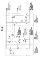
- a level conversion circuit includes an emitter follower section 101, an amplitude amplification section 102, and a level conversion section 103.
- the emitter follower section 101 is an emitter follower constructed such that the base of an NPN transistor Q1 is connected to an input terminal IN, the collector is connected to a high power-supply terminal VCC, and the connection node 001 of the emitter is connected to a first low power-supply terminal GND1 through a resistor R1.
- the amplitude amplification section 102 is a differential amplifier constructed such that the gate of an N-channel MOS transistor M1 is connected to the node 001, the connection node 002 of the drain is connected to the high power-supply terminal VCC through a resistor R2, and the source is connected to a node 004.
- the base of an N-channel MOS transistor M2 is connected to a reference power-supply terminal VR, the connection node 003 of the drain is connected to the high power-supply terminal VCC through a resistor R3, and the source is connected to a node 004.
- the base of an NPN transistor Q4 is connected to a reference power-supply terminal VCSI, the collector is connected to the node 004, and the emitter is connected to the first low power-supply terminal GND1 through a resistor R4.
- the level conversion section 103 is a level conversion section constructed such that the gate of a P-channel MOS transistor P1 is connected to the node 003, the source is connected to the high power-supply terminal VCC, and the drain is connected to a node 006.
- the gate of a P-channel MOS transistor P2 is connected to the node 002, the source is connected to the high power-supply terminal VCC, and the drain is connected to an output terminal OUT,
- the gate and drain of an N-channel MOS transistor N1 are connected to a node 006, and the source is connected to a second low power-supply terminal GND2.
- the gate of an N-channel MOS transistor N2 is connected to the node 006, the source is connected to the second low power-supply terminal GND2, and the drain is connected to the output terminal OUT.
- the level of the signal is shifted by the amount of the ON-state base-emitter voltage of the NPN transistor by the emitter follower section 101.
- the shifted signal is input to the node 001 which is the input of the amplitude amplification section 102, and the N-channel MOS transistor M1 is turned on.
- the N-channel MOS transistor M2 is turned off and current flows through the resistor R2.
- a level lower by the amount of the voltage drop of the resistor than the high power-supply potential is output to the node 002, and the high power-supply potential is output to the node 003.
- the P-channel MOS transistor P2 is turned on and the P-channel MOS transistor P1 is turned off.
- the electric charges on the node 006 are pulled out by the N-channel MOS transistor N1, and the N-channel MOS transistor N2 is turned off.
- the high level of the same CMOS level as the high power supply potential is output to the output terminal OUT.
- the low level of the CML level lower by the amount of a logic amplitude than the high power-supply potential is input to the input terminal IN, the low level of the same CMOS level as the second low power-supply potential is output to the output terminal OUT.
- MOS transistors are used in the transistors which constitute the current switches of the amplitude amplification section. Therefore, in the case where an output level is set to a sufficiently low value so that the input transistors P1 and P2 of the level conversion section 103 can be completely turned on or off when the low level on the output of the amplitude amplification section 102 fluctuates and assumes the highest value, the output level can be set to a sufficiently low value without causing a reduction in an operating speed which is caused due to saturation, unlike bipolar transistors, even when the low level on the output fluctuates conversely in the lowest direction, and consequently the high-speed operation of the level conversion section 103 also becomes possible. Because a low level can be output at the logic amplitude section without reducing the level of an input signal, it is possible to operate the NPN transistor of the current source without saturating it even at a low voltage.
- the level conversion circuit according to the present invention constitutes the current switches of the differential amplifier, which is the amplitude amplification section, by MOS transistors, whereby there is no reduction in the speed which is caused by the saturation of the current switches resulting from a fluctuation in the output level in the amplitude amplification section and the output level can be set so as to be sufficiently low. Accordingly, there is the advantage that high-speed operation is made possible even when power-supply voltage is reduced.
Landscapes
- Engineering & Computer Science (AREA)
- Computer Hardware Design (AREA)
- Physics & Mathematics (AREA)
- Computing Systems (AREA)
- General Engineering & Computer Science (AREA)
- Mathematical Physics (AREA)
- Logic Circuits (AREA)
- Amplifiers (AREA)
- Manipulation Of Pulses (AREA)
Applications Claiming Priority (3)
| Application Number | Priority Date | Filing Date | Title |
|---|---|---|---|
| JP5905/96 | 1996-01-17 | ||
| JP8005905A JPH09200004A (ja) | 1996-01-17 | 1996-01-17 | レベル変換回路 |
| JP590596 | 1996-01-17 |
Publications (2)
| Publication Number | Publication Date |
|---|---|
| EP0785629A1 EP0785629A1 (en) | 1997-07-23 |
| EP0785629B1 true EP0785629B1 (en) | 1999-12-22 |
Family
ID=11623923
Family Applications (1)
| Application Number | Title | Priority Date | Filing Date |
|---|---|---|---|
| EP97100638A Expired - Lifetime EP0785629B1 (en) | 1996-01-17 | 1997-01-16 | Level conversion circuit having differential circuit employing MOSFET |
Country Status (5)
| Country | Link |
|---|---|
| US (1) | US6340911B1 (ko) |
| EP (1) | EP0785629B1 (ko) |
| JP (1) | JPH09200004A (ko) |
| KR (1) | KR100236255B1 (ko) |
| DE (1) | DE69700965T2 (ko) |
Families Citing this family (8)
| Publication number | Priority date | Publication date | Assignee | Title |
|---|---|---|---|---|
| DE19930178C1 (de) * | 1999-06-30 | 2001-01-11 | Siemens Ag | ECL/CMOS-Pegelwandler |
| DE102004060212A1 (de) * | 2004-12-14 | 2006-07-06 | Infineon Technologies Ag | Pegelumsetzer |
| US9379709B2 (en) * | 2014-06-30 | 2016-06-28 | Finisar Corporation | Signal conversion |
| CN107086861B (zh) * | 2017-05-25 | 2023-11-10 | 北京航天动力研究所 | 一种电平转换双态输出驱动电路 |
| CN111191474B (zh) * | 2019-12-30 | 2023-04-25 | 成都达安众科技有限公司 | 一种rfid抗干扰解调器 |
| CN113595546B (zh) * | 2021-07-01 | 2022-05-17 | 深圳市汇芯通信技术有限公司 | 宽带高速电平转换电路及高速时钟芯片 |
| CN114400975B (zh) * | 2021-12-15 | 2022-09-27 | 陕西亚成微电子股份有限公司 | 一种基于包络追踪技术的功率放大电路及设计方法 |
| CN116827320B (zh) * | 2023-07-27 | 2024-01-26 | 江苏润石科技有限公司 | 一种快速响应的自适应电源转换电路 |
Family Cites Families (7)
| Publication number | Priority date | Publication date | Assignee | Title |
|---|---|---|---|---|
| JPH07118642B2 (ja) | 1986-01-08 | 1995-12-18 | 株式会社東芝 | レベル変換回路 |
| DE4000780C1 (ko) | 1990-01-12 | 1991-07-25 | Siemens Ag, 1000 Berlin Und 8000 Muenchen, De | |
| JPH04278719A (ja) * | 1991-03-06 | 1992-10-05 | Toshiba Corp | ソース電極結合形論理回路 |
| JPH05160709A (ja) | 1991-12-04 | 1993-06-25 | Hitachi Ltd | 高速論理入力回路 |
| EP0590818A3 (en) * | 1992-10-02 | 1994-05-11 | Nat Semiconductor Corp | Ecl-to-bicmos/cmos translator |
| US5332935A (en) * | 1993-04-12 | 1994-07-26 | Sierra Semiconductor | ECL and TTL to CMOS logic converter |
| US5434516A (en) | 1993-07-09 | 1995-07-18 | Future Domain Corporation | Automatic SCSI termination circuit |
-
1996
- 1996-01-17 JP JP8005905A patent/JPH09200004A/ja active Pending
-
1997
- 1997-01-16 EP EP97100638A patent/EP0785629B1/en not_active Expired - Lifetime
- 1997-01-16 US US08/784,775 patent/US6340911B1/en not_active Expired - Fee Related
- 1997-01-16 DE DE69700965T patent/DE69700965T2/de not_active Expired - Fee Related
- 1997-01-17 KR KR1019970001274A patent/KR100236255B1/ko not_active IP Right Cessation
Also Published As
| Publication number | Publication date |
|---|---|
| KR100236255B1 (ko) | 1999-12-15 |
| DE69700965T2 (de) | 2000-07-27 |
| US6340911B1 (en) | 2002-01-22 |
| KR970060698A (ko) | 1997-08-12 |
| JPH09200004A (ja) | 1997-07-31 |
| EP0785629A1 (en) | 1997-07-23 |
| DE69700965D1 (de) | 2000-01-27 |
Similar Documents
| Publication | Publication Date | Title |
|---|---|---|
| US4437171A (en) | ECL Compatible CMOS memory | |
| KR920003597B1 (ko) | 레벨변환회로 | |
| US4703203A (en) | BICMOS logic having three state output | |
| JP3079515B2 (ja) | ゲ−トアレイ装置及び入力回路及び出力回路及び降圧回路 | |
| US5900745A (en) | Semiconductor device including input buffer circuit capable of amplifying input signal with low amplitude in high speed and under low current consumption | |
| CA2051928A1 (en) | Apparatus and method for translating ecl signals to cmos signals | |
| US5929679A (en) | Voltage monitoring circuit capable of reducing power dissipation | |
| EP0785629B1 (en) | Level conversion circuit having differential circuit employing MOSFET | |
| EP0307323B1 (en) | Bipolar-complementary metal oxide semiconductor inverter | |
| US6281731B1 (en) | Control of hysteresis characteristic within a CMOS differential receiver | |
| US4716310A (en) | Logical biMOS gate circuit having low power dissipation | |
| US5315179A (en) | BICMOS level converter circuit | |
| EP0439158B1 (en) | High speed level conversion circuit | |
| US4806797A (en) | bi-CMOS buffer cascaded to CMOS driver having PMOS pull-up transistor with threshold voltage greater than VBE of bi-CMOS bipolar pull-up transistor | |
| EP0768762B1 (en) | Output circuit | |
| EP0529545B1 (en) | Level shifting CMOS integrated circuits | |
| US4977339A (en) | Semiconductor integrated circuit having a MOS transistor with a threshold level to enable a level conversion | |
| US5329183A (en) | ECL-CMOS level converter circuit | |
| US5945843A (en) | Semiconductor integrated circuit | |
| US5132566A (en) | BiMOS semiconductor integrated circuit having short-circuit protection | |
| KR940005975B1 (ko) | 출력회로 | |
| US5289061A (en) | Output gate for a semiconductor IC | |
| US5218244A (en) | Logic level converter circuit | |
| JP2864949B2 (ja) | レベル変換回路 | |
| JPH0645910A (ja) | BiCMOS論理回路 |
Legal Events
| Date | Code | Title | Description |
|---|---|---|---|
| PUAI | Public reference made under article 153(3) epc to a published international application that has entered the european phase |
Free format text: ORIGINAL CODE: 0009012 |
|
| 17P | Request for examination filed |
Effective date: 19970512 |
|
| AK | Designated contracting states |
Kind code of ref document: A1 Designated state(s): DE FR |
|
| 17Q | First examination report despatched |
Effective date: 19970917 |
|
| GRAG | Despatch of communication of intention to grant |
Free format text: ORIGINAL CODE: EPIDOS AGRA |
|
| GRAG | Despatch of communication of intention to grant |
Free format text: ORIGINAL CODE: EPIDOS AGRA |
|
| GRAH | Despatch of communication of intention to grant a patent |
Free format text: ORIGINAL CODE: EPIDOS IGRA |
|
| GRAH | Despatch of communication of intention to grant a patent |
Free format text: ORIGINAL CODE: EPIDOS IGRA |
|
| GRAA | (expected) grant |
Free format text: ORIGINAL CODE: 0009210 |
|
| AK | Designated contracting states |
Kind code of ref document: B1 Designated state(s): DE FR |
|
| REF | Corresponds to: |
Ref document number: 69700965 Country of ref document: DE Date of ref document: 20000127 |
|
| ET | Fr: translation filed | ||
| PLBE | No opposition filed within time limit |
Free format text: ORIGINAL CODE: 0009261 |
|
| STAA | Information on the status of an ep patent application or granted ep patent |
Free format text: STATUS: NO OPPOSITION FILED WITHIN TIME LIMIT |
|
| 26N | No opposition filed | ||
| PGFP | Annual fee paid to national office [announced via postgrant information from national office to epo] |
Ref country code: FR Payment date: 20030110 Year of fee payment: 7 |
|
| PGFP | Annual fee paid to national office [announced via postgrant information from national office to epo] |
Ref country code: DE Payment date: 20030123 Year of fee payment: 7 |
|
| REG | Reference to a national code |
Ref country code: FR Ref legal event code: TP |
|
| PG25 | Lapsed in a contracting state [announced via postgrant information from national office to epo] |
Ref country code: DE Free format text: LAPSE BECAUSE OF NON-PAYMENT OF DUE FEES Effective date: 20040803 |
|
| PG25 | Lapsed in a contracting state [announced via postgrant information from national office to epo] |
Ref country code: FR Free format text: LAPSE BECAUSE OF NON-PAYMENT OF DUE FEES Effective date: 20040930 |
|
| REG | Reference to a national code |
Ref country code: FR Ref legal event code: ST |