EP0785629A1 - Level conversion circuit having differential circuit employing MOSFET - Google Patents
Level conversion circuit having differential circuit employing MOSFET Download PDFInfo
- Publication number
- EP0785629A1 EP0785629A1 EP97100638A EP97100638A EP0785629A1 EP 0785629 A1 EP0785629 A1 EP 0785629A1 EP 97100638 A EP97100638 A EP 97100638A EP 97100638 A EP97100638 A EP 97100638A EP 0785629 A1 EP0785629 A1 EP 0785629A1
- Authority
- EP
- European Patent Office
- Prior art keywords
- drain
- mos transistor
- coupled
- supply terminal
- level
- Prior art date
- Legal status (The legal status is an assumption and is not a legal conclusion. Google has not performed a legal analysis and makes no representation as to the accuracy of the status listed.)
- Granted
Links
Images

Classifications
-
- H—ELECTRICITY
- H03—ELECTRONIC CIRCUITRY
- H03K—PULSE TECHNIQUE
- H03K19/00—Logic circuits, i.e. having at least two inputs acting on one output; Inverting circuits
- H03K19/0175—Coupling arrangements; Interface arrangements
-
- H—ELECTRICITY
- H03—ELECTRONIC CIRCUITRY
- H03K—PULSE TECHNIQUE
- H03K19/00—Logic circuits, i.e. having at least two inputs acting on one output; Inverting circuits
- H03K19/0175—Coupling arrangements; Interface arrangements
- H03K19/017509—Interface arrangements
- H03K19/017518—Interface arrangements using a combination of bipolar and field effect transistors [BIFET]
- H03K19/017527—Interface arrangements using a combination of bipolar and field effect transistors [BIFET] with at least one differential stage
Definitions
- the present invention relates to a level conversion circuit and, more particularly, to such a circuit that converts an ECL level or CML level signal to a MOS level signal.
- a level conversion circuit is widely employed to convert an input signal having an ECL level or a CML level signal to into an internal signal having a MOS level signal.
- Such a circuit generally employs a differential circuit composed of bipolar transistors.
- a conventional level conversion circuit includes an emitter follower section 101, an amplitude amplification section 102, and a level conversion section 103.
- the emitter follower section 101 is an emitter follower constructed such that the base of an NPN transistor Q1 is connected to an input terminal IN, the collector is connected to a high power-supply terminal VCC, and the connection node 001 of the emitter is connected to a first low power-supply terminal GND1 through a resistor R1.
- the amplitude amplification section 102 is a differential amplifier constructed such that the base of an NPN transistor Q2 is connected to the node 001, the connection node 002 of the collector is connected to the high power-supply terminal VCC through a resistor R2, and the emitter is connected to a node 004.
- the base of an NPN transistor Q3 is connected to a reference power-supply terminal VR, the connection node 003 of the collector is connected to the high power-supply terminal VCC through a resistor R3, and the emitter is connected to a node 004.
- the base of an NPN transistor Q4 is connected to a reference power-supply terminal VCSI, the collector is connected to the node 004, and the emitter is connected to the first low power-supply terminal GND1 through a resistor R4.
- the level conversion section 103 is a level conversion section constructed such that the gate of a P-channel MOS transistor P1 is connected to the node 003, the source is connected to the high power-supply terminal VCC, and the drain is connected to a node 006.
- the gate of a P-channel MOS transistor P2 is connected to the node 002, the source is connected to the high power-supply terminal VCC, and the drain is connected to an output terminal OUT.
- the gate and drain of an N-channel MOS transistor N1 are connected to a node 006, and the source is connected to a second low power-supply terminal GND2.
- the gate of an N-channel MOS transistor N2 is connected to the node 006, the source is connected to the second low power-supply terminal GND2, and the drain is connected to the output terminal OUT.
- the level of the signal is shifted by the amount of the ON-state base-emitter voltage of the NPN transistor by the emitter follower section 101.
- the shifted signal is input to the node 001 which is the input of the amplitude amplification section 102, and the NPN transistor Q2 is turned on.
- the NPN transistor Q3 is turned off and current flows through the resistor R2.
- a level lower by the amount of the voltage drop of the resistor than the high power-supply potential is output to the node 002, and the high power-supply potential is output to the node 003.
- These levels are input to the level conversion section 103.
- the P-channel MOS transistor P2 is turned on and the P-channel MOS transistor P1 is turned off.
- the electric charges on the node 006 are pulled out by the N-channel MOS transistor N1, and the N-channel MOS transistor N2 is turned off.
- the high level of the same CMOS level as the high power-supply potential is output to the output terminal OUT.
- the low level of the CML level lower by the amount of a logic amplitude than the high power-supply potential is input to the input terminal IN, the low level of the same CMOS level as the second low power-supply potential is output to the output terminal OUT.
- the low level on the output of the amplitude amplification section 102 must be a sufficiently low level so that one transistor of the input transistors of the level conversion section 103 can be completely turned on even when the value fluctuates and becomes the highest value.
- the low level of the output is set to a sufficiently low value in view of the case where it is the maximum value, there will be the problem that the collector potentials of the NPN transistors Q2 and Q3, which constitute the current switches of the amplitude amplification section 102, will be overreduced and that the transistors will be saturated and the operating speeds will be reduced, when the low level of the output fluctuates conversely in the lowest direction.
- a level conversion circuit includes an emitter follower section for receiving an ECL or a CML level signal and outputting a level-shifted signal, a differential amplitude amplification section provided with a pair of MOS transistors of one channel type, their sources being connected in common and also being connected to a first low power-supply terminal through a current source, an output of said emitter follower section being input to the gate of one transistor of the pair of MOS transistors, a complementary signal of the output of the emitter follower section or an input reference voltage being input to the gate of the other transistor, and their drains being connected to a high power-supply terminal through road devices, respectively and outputting differentially.
- the circuit further includes a level conversion section provided with a current mirror circuit which comprises a pair of MOS transistors of an opposite channel type, where their sources are connected to the high power-supply terminal and their gates receive a differential output of the amplitude amplification section and a pair of MOS transistors of the one channel type having their drains respectively connected to the drains of the MOS transistors, sources connected to a second low power-supply terminal, and gates connected in common and also connected to one drain thereof.
- a level conversion section provided with a current mirror circuit which comprises a pair of MOS transistors of an opposite channel type, where their sources are connected to the high power-supply terminal and their gates receive a differential output of the amplitude amplification section and a pair of MOS transistors of the one channel type having their drains respectively connected to the drains of the MOS transistors, sources connected to a second low power-supply terminal, and gates connected in common and also connected to one drain thereof.
- a level conversion circuit includes an emitter follower section 101, an amplitude amplification section 102, and a level conversion section 103.
- the emitter follower section 101 is an emitter follower constructed such that the base of an NPN transistor Q1 is connected to an input terminal IN, the collector is connected to a high power-supply terminal VCC, and the connection node 001 of the emitter is connected to a first low power-supply terminal GND1 through a resistor R1.
- the amplitude amplification section 102 is a differential amplifier constructed such that the gate of an N-channel MOS transistor M1 is connected to the node 001, the connection node 002 of the drain is connected to the high power-supply terminal VCC through a resistor R2, and the source is connected to a node 004.
- the base of an N-channel MOS transistor M2 is connected to a reference power-supply terminal VR, the connection node 003 of the drain is connected to the high power-supply terminal VCC through a resistor R3, and the source is connected to a node 004.
- the base of an NPN transistor Q4 is connected to a reference power-supply terminal VCSI, the collector is connected to the node 004, and the emitter is connected to the first low power-supply terminal GND1 through a resistor R4.
- the level conversion section 103 is a level conversion section constructed such that the gate of a P-channel MOS transistor P1 is connected to the node 003, the source is connected to the high power-supply terminal VCC, and the drain is connected to a node 006.
- the gate of a P-channel MOS transistor P2 is connected to the node 002, the source is connected to the high power-supply terminal VCC, and the drain is connected to an output terminal OUT,
- the gate and drain of an N-channel MOS transistor N1 are connected to a node 006, and the source is connected to a second low power-supply terminal GND2.
- the gate of an N-channel MOS transistor N2 is connected to the node 006, the source is connected to the second low power-supply terminal GND2, and the drain is connected to the output terminal OUT.
- the level of the signal is shifted by the amount of the ON-state base-emitter voltage of the NPN transistor by the emitter follower section 101.
- the shifted signal is input to the node 001 which is the input of the amplitude amplification section 102, and the N-channel MOS transistor M1 is turned on.
- the N-channel MOS transistor M2 is turned off and current flows through the resistor R2.
- a level lower by the amount of the voltage drop of the resistor than the high power-supply potential is output to the node 002, and the high power-supply potential is output to the node 003.
- the P-channel MOS transistor P2 is turned on and the P-channel MOS transistor P1 is turned off.
- the electric charges on the node 006 are pulled out by the N-channel MOS transistor N1, and the N-channel MOS transistor N2 is turned off.
- the high level of, the same CMOS level as the high power supply potential is output to the output terminal OUT.
- the low level of the CML level lower by the amount of a logic amplitude than the high power-supply potential is input to the input terminal IN, the low level of the same CMOS level as the second low power-supply potential is output to the output terminal OUT.
- MOS transistors are used in the transistors which constitute the current switches of the amplitude amplification section. Therefore, in the case where an output level is set to a sufficiently low value so that the input transistors P1 and P2 of the level conversion section 103 can be completely turned on or off when the low level on the output of the amplitude amplification section 102 fluctuates and assumes the highest value, the output level can be set to a sufficiently low value without causing a reduction in an operating speed which is caused due to saturation, unlike bipolar transistors, even when the low level on the output fluctuates conversely in the lowest direction, and consequently the high-speed operation of the level conversion section 103 also becomes possible. Because a low level can be output at the logic amplitude section without reducing the level of an input signal, it is possible to operate the NPN transistor of the current source without saturating it even at a low voltage.
- the level conversion circuit according to the present invention constitutes the current switches of the differential amplifier, which is the amplitude amplification section, by MOS transistors, whereby there is no reduction in the speed which is caused by the saturation of the current switches resulting from a fluctuation in the output level in the amplitude amplification section and the output level can be set so as to be sufficiently low. Accordingly, there is the advantage that high-speed operation is made possible even when power-supply voltage is reduced.
Abstract
Description
- The present invention relates to a level conversion circuit and, more particularly, to such a circuit that converts an ECL level or CML level signal to a MOS level signal.
- As a signal input circuit of a MOS-IC or MOS-LSI, a level conversion circuit is widely employed to convert an input signal having an ECL level or a CML level signal to into an internal signal having a MOS level signal. Such a circuit generally employs a differential circuit composed of bipolar transistors.
- Specifically, as shown in Fig. 2, a conventional level conversion circuit includes an
emitter follower section 101, anamplitude amplification section 102, and alevel conversion section 103. Theemitter follower section 101 is an emitter follower constructed such that the base of an NPN transistor Q1 is connected to an input terminal IN, the collector is connected to a high power-supply terminal VCC, and theconnection node 001 of the emitter is connected to a first low power-supply terminal GND1 through a resistor R1. - The
amplitude amplification section 102 is a differential amplifier constructed such that the base of an NPN transistor Q2 is connected to thenode 001, theconnection node 002 of the collector is connected to the high power-supply terminal VCC through a resistor R2, and the emitter is connected to anode 004. The base of an NPN transistor Q3 is connected to a reference power-supply terminal VR, theconnection node 003 of the collector is connected to the high power-supply terminal VCC through a resistor R3, and the emitter is connected to anode 004. The base of an NPN transistor Q4 is connected to a reference power-supply terminal VCSI, the collector is connected to thenode 004, and the emitter is connected to the first low power-supply terminal GND1 through a resistor R4. - The
level conversion section 103 is a level conversion section constructed such that the gate of a P-channel MOS transistor P1 is connected to thenode 003, the source is connected to the high power-supply terminal VCC, and the drain is connected to anode 006. The gate of a P-channel MOS transistor P2 is connected to thenode 002, the source is connected to the high power-supply terminal VCC, and the drain is connected to an output terminal OUT. The gate and drain of an N-channel MOS transistor N1 are connected to anode 006, and the source is connected to a second low power-supply terminal GND2. The gate of an N-channel MOS transistor N2 is connected to thenode 006, the source is connected to the second low power-supply terminal GND2, and the drain is connected to the output terminal OUT. - In operation, when the high level of the same current mode logic (CML) level as the high power-supply potential is input to the input terminal IN, the level of the signal is shifted by the amount of the ON-state base-emitter voltage of the NPN transistor by the
emitter follower section 101. The shifted signal is input to thenode 001 which is the input of theamplitude amplification section 102, and the NPN transistor Q2 is turned on. The NPN transistor Q3 is turned off and current flows through the resistor R2. A level lower by the amount of the voltage drop of the resistor than the high power-supply potential is output to thenode 002, and the high power-supply potential is output to thenode 003. These levels are input to thelevel conversion section 103. The P-channel MOS transistor P2 is turned on and the P-channel MOS transistor P1 is turned off. The electric charges on thenode 006 are pulled out by the N-channel MOS transistor N1, and the N-channel MOS transistor N2 is turned off. The high level of the same CMOS level as the high power-supply potential is output to the output terminal OUT. - When the low level of the CML level lower by the amount of a logic amplitude than the high power-supply potential is input to the input terminal IN, the low level of the same CMOS level as the second low power-supply potential is output to the output terminal OUT.
- In this conventional level conversion circuit, the levels on the
nodes amplitude amplification section 102, have to be sufficiently low in order to completely turn on one transistor of the P-channel MOS transistors P1 and P2 of the input section of thelevel conversion section 103 and completely turn off the other transistor. If this requirement is not met, the level conversion section will not be operated, or even if it were operated, the operating speed would become slow. - The low level on the output of the
amplitude amplification section 102 must be a sufficiently low level so that one transistor of the input transistors of thelevel conversion section 103 can be completely turned on even when the value fluctuates and becomes the highest value. However, if the low level of the output is set to a sufficiently low value in view of the case where it is the maximum value, there will be the problem that the collector potentials of the NPN transistors Q2 and Q3, which constitute the current switches of theamplitude amplification section 102, will be overreduced and that the transistors will be saturated and the operating speeds will be reduced, when the low level of the output fluctuates conversely in the lowest direction. - In order to avoid the saturation of the NPN transistors Q2 and Q3 at the current switch section of the
amplitude amplification section 102, there is a method where a diode is inserted between the emitter of the NPN transistor Q1 and thenode 001 so that the input signal level to a transistor constituting the current switch section is further reduced by the amount of the ON-state base-emitter voltage of the transistor. When the first low power-supply terminal GND2 is sufficiently low and the potential on the reference power-supply terminal VCSI is also low, there is no problem. However, when the first power-supply potential GND1 is high and becomes equal to the potential of the second low power-supply terminal GND2 and when the power-supply voltage, which is the potential difference between the high power-supply potential and the low power-supply potential, is low, there arises the problem that the collector potential of the NPN transistor Q4 constituting a current source falls and that the NPN transistor Q4 is saturated, if an input signal level is lowered. - Making the low level on the output of the
amplitude amplification section 102 sufficiently large so that the MOS transistors P1 and P2 of thelevel conversion section 103 can be completely turned on or off and also preventing the saturation of the transistors of the current switch and current source sections become even more severe as the power-supply voltage becomes lower. - Accordingly, it is an object of the present invention to provide a level conversion circuit which operates at high speeds even at a low power-supply voltage.
- A level conversion circuit according to the present invention includes an emitter follower section for receiving an ECL or a CML level signal and outputting a level-shifted signal, a differential amplitude amplification section provided with a pair of MOS transistors of one channel type, their sources being connected in common and also being connected to a first low power-supply terminal through a current source, an output of said emitter follower section being input to the gate of one transistor of the pair of MOS transistors, a complementary signal of the output of the emitter follower section or an input reference voltage being input to the gate of the other transistor, and their drains being connected to a high power-supply terminal through road devices, respectively and outputting differentially. The circuit further includes a level conversion section provided with a current mirror circuit which comprises a pair of MOS transistors of an opposite channel type, where their sources are connected to the high power-supply terminal and their gates receive a differential output of the amplitude amplification section and a pair of MOS transistors of the one channel type having their drains respectively connected to the drains of the MOS transistors, sources connected to a second low power-supply terminal, and gates connected in common and also connected to one drain thereof.
- The present invention will be described in further detail with reference to the accompanying drawings, in which:
- FIG. 1 is a circuit diagram showing an embodiment of a level conversion circuit of the present invention; and
- FIG. 2 is a circuit diagram showing an example of a conventional level conversion circuit.
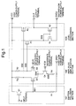
- Referring now to Fig. 1, a level conversion circuit according to an embodiment of the present invention includes an
emitter follower section 101, anamplitude amplification section 102, and alevel conversion section 103. Theemitter follower section 101 is an emitter follower constructed such that the base of an NPN transistor Q1 is connected to an input terminal IN, the collector is connected to a high power-supply terminal VCC, and theconnection node 001 of the emitter is connected to a first low power-supply terminal GND1 through a resistor R1. - The
amplitude amplification section 102 is a differential amplifier constructed such that the gate of an N-channel MOS transistor M1 is connected to thenode 001, theconnection node 002 of the drain is connected to the high power-supply terminal VCC through a resistor R2, and the source is connected to anode 004. The base of an N-channel MOS transistor M2 is connected to a reference power-supply terminal VR, theconnection node 003 of the drain is connected to the high power-supply terminal VCC through a resistor R3, and the source is connected to anode 004. The base of an NPN transistor Q4 is connected to a reference power-supply terminal VCSI, the collector is connected to thenode 004, and the emitter is connected to the first low power-supply terminal GND1 through a resistor R4. - The
level conversion section 103 is a level conversion section constructed such that the gate of a P-channel MOS transistor P1 is connected to thenode 003, the source is connected to the high power-supply terminal VCC, and the drain is connected to anode 006. The gate of a P-channel MOS transistor P2 is connected to thenode 002, the source is connected to the high power-supply terminal VCC, and the drain is connected to an output terminal OUT, The gate and drain of an N-channel MOS transistor N1 are connected to anode 006, and the source is connected to a second low power-supply terminal GND2. The gate of an N-channel MOS transistor N2 is connected to thenode 006, the source is connected to the second low power-supply terminal GND2, and the drain is connected to the output terminal OUT. - In operation, when the high level of the same current mode logic (CML) level as the high power-supply potential is input to the input terminal IN, the level of the signal is shifted by the amount of the ON-state base-emitter voltage of the NPN transistor by the
emitter follower section 101. The shifted signal is input to thenode 001 which is the input of theamplitude amplification section 102, and the N-channel MOS transistor M1 is turned on. The N-channel MOS transistor M2 is turned off and current flows through the resistor R2. A level lower by the amount of the voltage drop of the resistor than the high power-supply potential is output to thenode 002, and the high power-supply potential is output to thenode 003. These levels are input to thelevel conversion section 103. The P-channel MOS transistor P2 is turned on and the P-channel MOS transistor P1 is turned off. The electric charges on thenode 006 are pulled out by the N-channel MOS transistor N1, and the N-channel MOS transistor N2 is turned off. The high level of, the same CMOS level as the high power supply potential is output to the output terminal OUT. - When the low level of the CML level lower by the amount of a logic amplitude than the high power-supply potential is input to the input terminal IN, the low level of the same CMOS level as the second low power-supply potential is output to the output terminal OUT.
- In the level conversion circuit of the embodiment of the present invention, MOS transistors are used in the transistors which constitute the current switches of the amplitude amplification section. Therefore, in the case where an output level is set to a sufficiently low value so that the input transistors P1 and P2 of the
level conversion section 103 can be completely turned on or off when the low level on the output of theamplitude amplification section 102 fluctuates and assumes the highest value, the output level can be set to a sufficiently low value without causing a reduction in an operating speed which is caused due to saturation, unlike bipolar transistors, even when the low level on the output fluctuates conversely in the lowest direction, and consequently the high-speed operation of thelevel conversion section 103 also becomes possible. Because a low level can be output at the logic amplitude section without reducing the level of an input signal, it is possible to operate the NPN transistor of the current source without saturating it even at a low voltage. - As has been described above, the level conversion circuit according to the present invention constitutes the current switches of the differential amplifier, which is the amplitude amplification section, by MOS transistors, whereby there is no reduction in the speed which is caused by the saturation of the current switches resulting from a fluctuation in the output level in the amplitude amplification section and the output level can be set so as to be sufficiently low. Accordingly, there is the advantage that high-speed operation is made possible even when power-supply voltage is reduced.
- While the invention has been described with reference to a preferred embodiment thereof, the invention is not to be limited to the details given herein, but may be modified within the scope of the appended claim.
Claims (3)
- A level conversion circuit comprising a first MOS transistor of a first channel type having a gate coupled to a first input terminal, a source coupled to a current source and a drain coupled to a first load resistor, a second MOS transistor of said first channel type having a gate coupled to a second input terminal, a source coupled to said current source and a drain coupled to a second load resistor, a third MOS transistor of a second channel type having a gate coupled to the drain of said first MOS transistor, a source coupled to a first potential line and a drain, a fourth MOS transistor of said second channel type having a gate coupled to the drain of said second MOS transistor, a source coupled to said first potential line and a drain, a fifth MOS transistor of said first channel type having a gate coupled to the drain of said third MOS transistor, a drain coupled to the drain of said third MOS transistor and a source coupled to a second potential line, a sixth MOS transistor of said first channel type having a gate coupled to the gate of said fifth MOS transistor, a drain coupled to the drain of said fourth MOS transistor and a source coupled to said second potential line, and an output terminal coupled to the drain of said fourth MOS transistor.
- The circuit as claimed in claim 1, wherein said first channel type is an N channel type and said second channel type is a P channel type.
- A level conversion circuit for converting an ECL or CML level signal to a MOS level signal, comprising:an emitter follower section for receiving said ECL or CML level signal and outputtting a level-shifted signal;a differential amplitude amplification section provided with a pair of N-channel MOS transistors, their sources being connected in common and also being connected to a first low power-supply terminal through a current source, an output of said emitter follower section being input to the gate of one transistor of said pair of N-channel MOS transistors, a complementary signal of the output of said emitter follower section or an input reference voltage being input to the gate of the other transistor, and their drains being connected to a high power-supply terminal through road devices, respectively; anda level conversion section provided with a pair of P-channel MOS transistors where their sources are connected to said high power-supply terminal and their gates receive a differential output of said amplitude amplification section and a current mirror circuit which comprises a pair of N-channel MOS transistors where their drains are respectively connected to the drains of said P-channel MOS transistors, the sources of the N-channel MOS transistors being connected to a second low power-supply terminal, the gates of the N-channel MOS transistors being connected in common and also being connected to one drain of the N-channel MOS transistors, and the other drain being output.
Applications Claiming Priority (3)
| Application Number | Priority Date | Filing Date | Title |
|---|---|---|---|
| JP8005905A JPH09200004A (en) | 1996-01-17 | 1996-01-17 | Level conversion circuit |
| JP5905/96 | 1996-01-17 | ||
| JP590596 | 1996-01-17 |
Publications (2)
| Publication Number | Publication Date |
|---|---|
| EP0785629A1 true EP0785629A1 (en) | 1997-07-23 |
| EP0785629B1 EP0785629B1 (en) | 1999-12-22 |
Family
ID=11623923
Family Applications (1)
| Application Number | Title | Priority Date | Filing Date |
|---|---|---|---|
| EP97100638A Expired - Lifetime EP0785629B1 (en) | 1996-01-17 | 1997-01-16 | Level conversion circuit having differential circuit employing MOSFET |
Country Status (5)
| Country | Link |
|---|---|
| US (1) | US6340911B1 (en) |
| EP (1) | EP0785629B1 (en) |
| JP (1) | JPH09200004A (en) |
| KR (1) | KR100236255B1 (en) |
| DE (1) | DE69700965T2 (en) |
Cited By (4)
| Publication number | Priority date | Publication date | Assignee | Title |
|---|---|---|---|---|
| DE19930178C1 (en) * | 1999-06-30 | 2001-01-11 | Siemens Ag | Integrated circuit-type signal level changing circuit especially based on ECL-CMOS elements |
| WO2016004112A1 (en) * | 2014-06-30 | 2016-01-07 | Finisar Corporation | Signal conversion |
| CN107086861A (en) * | 2017-05-25 | 2017-08-22 | 北京航天动力研究所 | A kind of level conversion bifurcation output driving circuit |
| CN114400975A (en) * | 2021-12-15 | 2022-04-26 | 陕西亚成微电子股份有限公司 | Power amplification circuit based on envelope tracking technology and design method |
Families Citing this family (4)
| Publication number | Priority date | Publication date | Assignee | Title |
|---|---|---|---|---|
| DE102004060212A1 (en) * | 2004-12-14 | 2006-07-06 | Infineon Technologies Ag | Level converter for signal processing circuits has amplifier which generates difference signal after comparing potential at output with reference potential on which control signal is dependent |
| CN111191474B (en) * | 2019-12-30 | 2023-04-25 | 成都达安众科技有限公司 | RFID anti-interference demodulator |
| CN113595546B (en) * | 2021-07-01 | 2022-05-17 | 深圳市汇芯通信技术有限公司 | Broadband high-speed level switching circuit and high-speed clock chip |
| CN116827320B (en) * | 2023-07-27 | 2024-01-26 | 江苏润石科技有限公司 | Fast-response self-adaptive power supply conversion circuit |
Citations (4)
| Publication number | Priority date | Publication date | Assignee | Title |
|---|---|---|---|---|
| US4779016A (en) * | 1986-01-08 | 1988-10-18 | Kabushiki Kaisha Toshiba | Level conversion circuit |
| EP0436823A1 (en) * | 1990-01-12 | 1991-07-17 | Siemens Aktiengesellschaft | Signal level converter |
| US5332935A (en) * | 1993-04-12 | 1994-07-26 | Sierra Semiconductor | ECL and TTL to CMOS logic converter |
| US5434518A (en) * | 1992-10-02 | 1995-07-18 | National Semiconductor Corporation | ECL-to-BICOMS/CMOS translator |
Family Cites Families (3)
| Publication number | Priority date | Publication date | Assignee | Title |
|---|---|---|---|---|
| JPH04278719A (en) * | 1991-03-06 | 1992-10-05 | Toshiba Corp | Source electrode coupled logic circuit |
| JPH05160709A (en) | 1991-12-04 | 1993-06-25 | Hitachi Ltd | High speed logic input circuit |
| US5434516A (en) | 1993-07-09 | 1995-07-18 | Future Domain Corporation | Automatic SCSI termination circuit |
-
1996
- 1996-01-17 JP JP8005905A patent/JPH09200004A/en active Pending
-
1997
- 1997-01-16 US US08/784,775 patent/US6340911B1/en not_active Expired - Fee Related
- 1997-01-16 EP EP97100638A patent/EP0785629B1/en not_active Expired - Lifetime
- 1997-01-16 DE DE69700965T patent/DE69700965T2/en not_active Expired - Fee Related
- 1997-01-17 KR KR1019970001274A patent/KR100236255B1/en not_active IP Right Cessation
Patent Citations (4)
| Publication number | Priority date | Publication date | Assignee | Title |
|---|---|---|---|---|
| US4779016A (en) * | 1986-01-08 | 1988-10-18 | Kabushiki Kaisha Toshiba | Level conversion circuit |
| EP0436823A1 (en) * | 1990-01-12 | 1991-07-17 | Siemens Aktiengesellschaft | Signal level converter |
| US5434518A (en) * | 1992-10-02 | 1995-07-18 | National Semiconductor Corporation | ECL-to-BICOMS/CMOS translator |
| US5332935A (en) * | 1993-04-12 | 1994-07-26 | Sierra Semiconductor | ECL and TTL to CMOS logic converter |
Cited By (8)
| Publication number | Priority date | Publication date | Assignee | Title |
|---|---|---|---|---|
| DE19930178C1 (en) * | 1999-06-30 | 2001-01-11 | Siemens Ag | Integrated circuit-type signal level changing circuit especially based on ECL-CMOS elements |
| WO2016004112A1 (en) * | 2014-06-30 | 2016-01-07 | Finisar Corporation | Signal conversion |
| US9379709B2 (en) | 2014-06-30 | 2016-06-28 | Finisar Corporation | Signal conversion |
| CN106575963A (en) * | 2014-06-30 | 2017-04-19 | 菲尼萨公司 | Signal conversion |
| CN106575963B (en) * | 2014-06-30 | 2020-04-10 | 菲尼萨公司 | Signal conversion |
| CN107086861A (en) * | 2017-05-25 | 2017-08-22 | 北京航天动力研究所 | A kind of level conversion bifurcation output driving circuit |
| CN107086861B (en) * | 2017-05-25 | 2023-11-10 | 北京航天动力研究所 | Level conversion binary output driving circuit |
| CN114400975A (en) * | 2021-12-15 | 2022-04-26 | 陕西亚成微电子股份有限公司 | Power amplification circuit based on envelope tracking technology and design method |
Also Published As
| Publication number | Publication date |
|---|---|
| EP0785629B1 (en) | 1999-12-22 |
| US6340911B1 (en) | 2002-01-22 |
| DE69700965T2 (en) | 2000-07-27 |
| KR970060698A (en) | 1997-08-12 |
| JPH09200004A (en) | 1997-07-31 |
| KR100236255B1 (en) | 1999-12-15 |
| DE69700965D1 (en) | 2000-01-27 |
Similar Documents
| Publication | Publication Date | Title |
|---|---|---|
| KR920003597B1 (en) | Level converting circuit | |
| US5625308A (en) | Two input-two output differential latch circuit | |
| US4703203A (en) | BICMOS logic having three state output | |
| US5900745A (en) | Semiconductor device including input buffer circuit capable of amplifying input signal with low amplitude in high speed and under low current consumption | |
| US5929679A (en) | Voltage monitoring circuit capable of reducing power dissipation | |
| US6340911B1 (en) | Level conversion circuit having differential circuit employing MOSFET | |
| EP0441317A1 (en) | Bi-CMOS logic gate circuits for low-voltage semiconductor integrated circuits | |
| EP0439158B1 (en) | High speed level conversion circuit | |
| US5371421A (en) | Low power BiMOS amplifier and ECL-CMOS level converter | |
| US6753707B2 (en) | Delay circuit and semiconductor device using the same | |
| EP0590247A2 (en) | BICMOS level converter circuit | |
| US20070194830A1 (en) | High performance level shift circuit with low input voltage | |
| EP0529545B1 (en) | Level shifting CMOS integrated circuits | |
| US5138195A (en) | Bi-CMOS logic circuit having full voltage swing and rapid turn-off | |
| US4977339A (en) | Semiconductor integrated circuit having a MOS transistor with a threshold level to enable a level conversion | |
| KR100310883B1 (en) | Input circuit | |
| US5329183A (en) | ECL-CMOS level converter circuit | |
| US5329185A (en) | CMOS logic circuitry providing improved operating speed | |
| US5162677A (en) | ECL to CMOS level conversion circuit | |
| US5945843A (en) | Semiconductor integrated circuit | |
| US5218244A (en) | Logic level converter circuit | |
| JP2795046B2 (en) | Output buffer circuit | |
| JP2864949B2 (en) | Level conversion circuit | |
| US5563543A (en) | Low-voltage BiCMOS digital delay chain suitable for operation over a wide power supply range | |
| JP3583359B2 (en) | Logic level conversion circuit |
Legal Events
| Date | Code | Title | Description |
|---|---|---|---|
| PUAI | Public reference made under article 153(3) epc to a published international application that has entered the european phase |
Free format text: ORIGINAL CODE: 0009012 |
|
| 17P | Request for examination filed |
Effective date: 19970512 |
|
| AK | Designated contracting states |
Kind code of ref document: A1 Designated state(s): DE FR |
|
| 17Q | First examination report despatched |
Effective date: 19970917 |
|
| GRAG | Despatch of communication of intention to grant |
Free format text: ORIGINAL CODE: EPIDOS AGRA |
|
| GRAG | Despatch of communication of intention to grant |
Free format text: ORIGINAL CODE: EPIDOS AGRA |
|
| GRAH | Despatch of communication of intention to grant a patent |
Free format text: ORIGINAL CODE: EPIDOS IGRA |
|
| GRAH | Despatch of communication of intention to grant a patent |
Free format text: ORIGINAL CODE: EPIDOS IGRA |
|
| GRAA | (expected) grant |
Free format text: ORIGINAL CODE: 0009210 |
|
| AK | Designated contracting states |
Kind code of ref document: B1 Designated state(s): DE FR |
|
| REF | Corresponds to: |
Ref document number: 69700965 Country of ref document: DE Date of ref document: 20000127 |
|
| ET | Fr: translation filed | ||
| PLBE | No opposition filed within time limit |
Free format text: ORIGINAL CODE: 0009261 |
|
| STAA | Information on the status of an ep patent application or granted ep patent |
Free format text: STATUS: NO OPPOSITION FILED WITHIN TIME LIMIT |
|
| 26N | No opposition filed | ||
| PGFP | Annual fee paid to national office [announced via postgrant information from national office to epo] |
Ref country code: FR Payment date: 20030110 Year of fee payment: 7 |
|
| PGFP | Annual fee paid to national office [announced via postgrant information from national office to epo] |
Ref country code: DE Payment date: 20030123 Year of fee payment: 7 |
|
| REG | Reference to a national code |
Ref country code: FR Ref legal event code: TP |
|
| PG25 | Lapsed in a contracting state [announced via postgrant information from national office to epo] |
Ref country code: DE Free format text: LAPSE BECAUSE OF NON-PAYMENT OF DUE FEES Effective date: 20040803 |
|
| PG25 | Lapsed in a contracting state [announced via postgrant information from national office to epo] |
Ref country code: FR Free format text: LAPSE BECAUSE OF NON-PAYMENT OF DUE FEES Effective date: 20040930 |
|
| REG | Reference to a national code |
Ref country code: FR Ref legal event code: ST |