EP0590247A2 - BICMOS level converter circuit - Google Patents
BICMOS level converter circuit Download PDFInfo
- Publication number
- EP0590247A2 EP0590247A2 EP93110587A EP93110587A EP0590247A2 EP 0590247 A2 EP0590247 A2 EP 0590247A2 EP 93110587 A EP93110587 A EP 93110587A EP 93110587 A EP93110587 A EP 93110587A EP 0590247 A2 EP0590247 A2 EP 0590247A2
- Authority
- EP
- European Patent Office
- Prior art keywords
- emitter
- coupled
- transistor
- power supply
- voltage level
- Prior art date
- Legal status (The legal status is an assumption and is not a legal conclusion. Google has not performed a legal analysis and makes no representation as to the accuracy of the status listed.)
- Granted
Links
- 239000000872 buffer Substances 0.000 claims abstract description 14
- 230000004044 response Effects 0.000 claims description 18
- 230000001105 regulatory effect Effects 0.000 claims description 7
- 230000007704 transition Effects 0.000 abstract 1
- 230000001419 dependent effect Effects 0.000 description 15
- 238000010586 diagram Methods 0.000 description 12
- 230000007423 decrease Effects 0.000 description 6
- 230000008901 benefit Effects 0.000 description 5
- 238000006243 chemical reaction Methods 0.000 description 3
- 230000002411 adverse Effects 0.000 description 2
- 230000008859 change Effects 0.000 description 2
- 230000000295 complement effect Effects 0.000 description 2
- 230000003247 decreasing effect Effects 0.000 description 2
- 238000000034 method Methods 0.000 description 1
- 238000012986 modification Methods 0.000 description 1
- 230000004048 modification Effects 0.000 description 1
- 230000009467 reduction Effects 0.000 description 1
- 239000004065 semiconductor Substances 0.000 description 1
Images


Classifications
-
- H—ELECTRICITY
- H03—ELECTRONIC CIRCUITRY
- H03K—PULSE TECHNIQUE
- H03K19/00—Logic circuits, i.e. having at least two inputs acting on one output; Inverting circuits
-
- H—ELECTRICITY
- H03—ELECTRONIC CIRCUITRY
- H03K—PULSE TECHNIQUE
- H03K19/00—Logic circuits, i.e. having at least two inputs acting on one output; Inverting circuits
- H03K19/003—Modifications for increasing the reliability for protection
- H03K19/00369—Modifications for compensating variations of temperature, supply voltage or other physical parameters
-
- H—ELECTRICITY
- H03—ELECTRONIC CIRCUITRY
- H03K—PULSE TECHNIQUE
- H03K19/00—Logic circuits, i.e. having at least two inputs acting on one output; Inverting circuits
- H03K19/01—Modifications for accelerating switching
- H03K19/013—Modifications for accelerating switching in bipolar transistor circuits
- H03K19/0136—Modifications for accelerating switching in bipolar transistor circuits by means of a pull-up or down element
-
- H—ELECTRICITY
- H03—ELECTRONIC CIRCUITRY
- H03K—PULSE TECHNIQUE
- H03K19/00—Logic circuits, i.e. having at least two inputs acting on one output; Inverting circuits
- H03K19/0175—Coupling arrangements; Interface arrangements
- H03K19/017509—Interface arrangements
- H03K19/017518—Interface arrangements using a combination of bipolar and field effect transistors [BIFET]
- H03K19/017527—Interface arrangements using a combination of bipolar and field effect transistors [BIFET] with at least one differential stage
Definitions
- This invention relates generally to logic level conversion, and more particularly, to a BICMOS level converter circuit.
- Integrated circuits are required to operate at increasingly lower power supply voltages and increasingly higher speeds. Integrated circuits are often used in applications where low power consumption and high speed are important, such as in a battery powered computer, or the like. An effective method for decreasing power consumption is to use a lower power supply voltage (for example, 3.3 volts).
- ECL emitter-coupled logic
- BINMOS complementary metal-oxide-semiconductor
- a BICMOS circuit combines bipolar transistors with CMOS (complementary metal-oxide-semiconductor) transistors on the same integrated circuit.
- CMOS complementary metal-oxide-semiconductor
- the bipolar transistors of a BICMOS circuit provide the advantage of high speed and high drive capability, while the CMOS transistors provide the advantage of reduced power consumption.
- a level conversion circuit converts, or translates, a logic signal from ECL logic levels to BINMOS logic levels.
- a level conversion circuit should not cause excessive delay or consume a large amount of power.
- a conventional BICMOS level converter has a differential amplifier, emitter-follower input transistors for receiving an ECL level logic signal, and emitter-follower output transistors.
- the differential amplifier includes NPN transistors having their emitters coupled together, and a resistor coupled between each of the collectors and a positive power supply voltage terminal.
- N-channel MOSFET current sources are used to supply a relatively constant current.
- the conventional BICMOS level converter designed to operate with a power supply voltage of 5.0 volts, may not work reliability with a 3.3 volt power supply.
- a 3.3 volt power supply is used instead of the 5.0 volt power supply, the operating margins of some of the transistors in the level converter circuit may be reduced.
- the margins are reduced in the conventional BICMOS level converter because a V BE voltage drop across a forward biased bipolar transistor is independent of the power supply voltage, and remains relatively constant. Therefore, when the power supply voltage is reduced, there may not be sufficient voltage range to allow for all of the V BE voltage drops without adversely affecting the operation of the circuit. Also, the integrated circuit may be more vulnerable to noise and to fluctuations in power supply voltages.
- the conventional BICMOS level converter may be considerably slower when operated at a lower power supply voltage, because the bipolar transistors of the ECL portion of the level converter may now be operating in the saturation operating region. If the bipolar transistors are allowed to operate in saturation, increased switching time, and an undesirable reduction in speed may result.
- a level converter for converting signals operating within a first predetermined voltage level range to a second predetermined voltage level range.
- the level converter includes a differential amplifier, a first emitter-follower circuit, a second emitter-follower circuit, and cross-coupled half-latch means.
- the differential amplifier is coupled to a first power supply voltage terminal, and includes first and second resistors and first and second bipolar transistors, and receives first and second input signals within the first predetermined voltage level range.
- the differential amplifier provides first and second differential signals.
- the first emitter-follower circuit is coupled to the differential amplifier and receives the first differential signal.
- the first emitter-follower circuit provides a third signal within the second predetermined voltage level range.
- the second emitter-follower circuit is coupled to the differential amplifier and receives the second differential signal. In response, the second emitter-follower circuit provides a fourth signal within the second predetermined voltage level range.
- the cross-coupled half-latch means is coupled to the first and second emitter-follower circuits, and reduces the fourth signal from a high voltage level to a low voltage level within the range of said second predetermined voltage level range in response to a high voltage level being provided by the second emitter-follower circuit.
- the cross-coupled half-latch also reduces the third signal from a high voltage level to a low voltage level within the range of the second predetermined voltage level range in response to a high voltage level being provided by the first emitter-follower circuit.
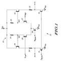
- FIG. 1 illustrates in schematic diagram form an input buffer in accordance with the present invention.
- FIG. 2 illustrates in schematic diagram form a power supply dependent bias voltage generator circuit in accordance with the present invention.
- FIG. 3 illustrates in partial schematic diagram form and partial logic diagram form a level converter in accordance with one embodiment of the present invention.
- FIG. 4 illustrates in partial schematic diagram form and partial logic diagram form a level converter in accordance with another embodiment of the present invention.
- FIG. 1 illustrates in schematic diagram form input buffer 20 in accordance with the present invention.
- Input buffer 20 includes differential amplifier 22, emitter-follower transistors 29 and 32, resistors 30 and 33, and N-channel transistors 31 and 34.
- Differential amplifier 22 includes resistors 24 and 25, NPN transistors 26 and 27, and N-channel transistor 28.
- Resistor 24 of differential amplifier 22 has a first terminal connected to a positive power supply voltage terminal labeled "V DD ", and a second terminal connected to node 101.
- Resistor 25 has a first terminal connected to V DD , and a second terminal connected to node 102.
- NPN transistor 26 has a collector connected to the second terminal of resistor 24 at node 101, a base for receiving an ECL level single-ended input signal labeled "A IN ", and an emitter.
- NPN transistor 27 has a collector connected to the second terminal of resistor 25 at node 102, a base for receiving a reference voltage labeled "V REF ", and emitter connected to the emitter of NPN transistor 26.
- N-channel transistor 28 has a drain connected to the emitters of NPN transistors 26 and 27, a gate for receiving a bias voltage labeled "N BIAS ", and a source connected to a negative power supply voltage terminal labeled "V SS ".
- Emitter-follower transistor 29 has a collector connected to V DD , a base connected to the second terminal of resistor 24 at node 101, and an emitter.
- Resistor 30 has a first terminal connected to the emitter of emitter-follower transistor 29, and a second terminal for providing a buffered signal labeled "A*".
- N-channel transistor 31 has a drain connected to the second terminal of resistor 30, a gate for receiving a power supply dependent bias voltage labeled "C BIAS ", and a source connected to V SS .
- Emitter-follower transistor 32 has a collector connected to V DD , a base connected to the second terminal of resistor 25 at node 102, and an emitter.
- Resistor 33 has a first terminal connected to the emitter of emitter-follower transistor 32, and a second terminal for providing a buffered signal labeled "A”.
- N-channel transistor 34 has a drain connected to the second terminal of resistor 33, a gate for receiving power supply dependent bias voltage C BIAS , and a source connected to V SS . Note that an asterisk (*) after the signal name indicates that the signal is active at a logic low.
- ECL level input signal A IN is received by input buffer 20 at the base of NPN transistor 26.
- ECL level input signal A IN swings between an ECL logic level high of 1.6 volts and an ECL logic low of about 0.8 volts.
- N-channel transistor 28 receives bias voltage N BIAS and provides a current source for differential amplifier 22.
- N BIAS is provided at about 1.2 to 1.4 volts.
- Reference voltage V REF is provided to the base of NPN transistor 27 at a voltage level approximately at the midpoint of the logic swing of ECL level input signal A IN . If input signal A IN is a logic low, it is more negative than reference voltage V REF , NPN transistor 26 will be substantially non-conductive and NPN transistor 27 will be conductive.
- a current designated as "I28”, through N-channel transistor 28, will be steered through NPN transistor 27, and the voltage at node 102 will be equal to V DD minus I28R25 where R25 is the resistance of resistor 25.
- the voltage at node 101 will be equal to approximately V DD since there is substantially no current flow through NPN transistor 26. If input signal A IN is equal to a logic high voltage, it is less negative than V REF , causing NPN transistor 26 to be conductive and NPN transistor 27 to be substantially non-conductive.
- Current I28 will be steered through NPN transistor 26 and the voltage at node 101 will be equal to V DD minus I28R24 where R24 is the resistance of resistor 24, and the voltage at node 102 will be equal to approximately V DD . Therefore, the difference between a logic high and a logic low voltage at nodes 101 and 102 of differential amplifier 22 is equal to the voltage drop across either of resistors 24 or 25. In the preferred embodiment, R24 is equal to approximately R25.
- Emitter-follower transistors 29 and 32 receive the voltage at nodes 101 and 102, respectively.
- the emitter of emitter-follower transistor 29 provides a voltage equal to the voltage at node 101 less one base-emitter diode voltage drop (V BE ), where one V BE is equal to approximately 0.8 volts.
- the emitter of transistor 32 provides a voltage equal to the voltage at node 102 less one V BE .
- Resistors 30 and 33 perform a level shift function by reducing the voltage provided by emitter-follower transistors 29 and 32. The amount of level shift, or voltage drop, provided by resistors 30 and 33 depends on the amount of current provided by N-channel transistors 31 and 34 and the resistance of resistors 30 and 33.
- Power supply dependent bias voltage C BIAS is provided to the gates of N-channel transistors 31 and 34, and determines the amount of current provided by N-channel transistors 31 and 34.
- N-channel transistors 31 and 34 function as power supply dependent current sources.
- Bias voltage C BIAS is variable, and dependent on power supply voltage V DD . That is, as V DD changes, bias voltage C BIAS changes. If V DD is chosen to be 3.3 volts, V DD may fluctuate between 2.8 and 4.0 volts. An increase in V DD causes bias voltage C BIAS to increase, and a decrease in V DD causes bias voltage C BIAS to decrease. When C BIAS increases, the current provided by N-channel transistors 31 and 34 increases.
- bias voltage C BIAS is chosen so that the drain-source current provided by N-channel transistors 31 and 34 causes buffered signals A and A* to remain constant with respect to V SS and independent of power supply voltage V DD .
- V DD is equal to about 3.0 volts
- the voltage drop across each of resistors 30 and 33 is equal to about 0.5 volts.
- V DD increases to about 3.5 volts
- the voltage drop across each of resistors 30 and 33 increases to about 1.0 volt.
- This causes buffered signals A and A* to always remain constant with respect to V SS , thereby ensuring that buffered signals A and A* have fixed margins independent of changes in V DD .
- the circuit that provides C BIAS is illustrated in FIG. 2 and will be discussed later. Providing buffered signals A and A* with respect to V SS allows ample margins on the following stages, even at low power supply voltages.
- buffered signals A and A* swing between a intermediate logic high voltage of 1.6 volts and a logic low voltage of 1.0 volt, and V SS is chosen to be ground.
- buffered signals A and A* are provided to level converter 60 of FIG. 3. Since buffered signals A and A* are referenced to V SS , better margins and increased signal swings in level converter 60 are realized.
- FIG. 2 illustrates in schematic diagram form, power supply dependent bias voltage generator circuit 40 in accordance with the present invention.
- Power supply dependent bias voltage circuit 40 includes resistors 41 and 54, NPN transistor 44, operational amplifier 46, N-channel transistors 42, 45, and 57, and current mirror 52.
- Operational amplifier 46 includes P-channel transistors 47 and 48, NPN transistors 49 and 50, and N-channel transistor 51.
- P-channel transistors 47 and 48 function as loads for operational amplifier 46.
- Current mirror 52 includes P-channel transistors 53 and 56.
- Resistor 41 has a first terminal connected to V DD , and a second terminal.
- N-channel transistor 42 has a drain connected to the second terminal of resistor 41, a gate for receiving N BIAS , and a source connected to V SS .
- NPN transistor 44 has a collector connected to V DD , a base connected to the second terminal of resistor 41, and an emitter connected to node 103.
- N-channel transistor 45 has a drain connected to the emitter of NPN transistor 44 at node 103, a gate for receiving power supply dependent bias voltage C BIAS , and a source connected to V SS .
- P-channel transistor 47 of operational amplifier 46 has a source connected to V DD , a gate, and a drain.
- P-channel transistor 48 has a source connected to V DD , and a gate and a drain connected to the gate of P-channel transistor 47.
- NPN transistor 49 has a collector connected to the drain of P-channel transistor 47, a base connected to the emitter of NPN transistor 44 at node 103, and an emitter.
- NPN transistor 50 has a collector connected to the drain of P-channel transistor 48, a base connected to node 104, and an emitter connected to the emitter of NPN transistor 49.
- N-channel transistor 51 has a drain connected to the emitters of NPN transistors 49 and 50, a gate for receiving bias voltage N BIAS , and a source connected to V SS .
- P-channel transistor 53 of current mirror 52 has a source connected to V DD , a gate connected to the drain of P-channel transistor 47, and a drain connected to the base of NPN transistor 50 at node 104.
- P-channel transistor 56 has a source connected to V DD , a gate connected to the gate of P-channel transistor 53, and a drain for providing power supply dependent bias voltage C BIAS .
- Resistor 54 has a first terminal connected to the base of transistor 50 at node 104, and a second terminal for receiving a band gap voltage labeled "V BG ".
- N-channel transistor 57 has a gate and a drain connected to the drain of P-channel transistor 56, and a source connected to V SS .
- N-channel transistor 42 and bias voltage N BIAS provide a relatively constant current source for resistor 41, making the voltage drop across resistor 41 relatively constant with respect to V DD .
- NPN transistor 44 provides a voltage to the base of NPN transistor 49 at node 103 approximately equal to the voltage at the second terminal of resistor 41, less one V BE . Since the voltage drop across resistor 41 is relatively constant with respect to V DD , the voltage at node 103 is also relatively constant with respect to V DD .
- P-channel transistors 47 and 48 form a current mirror, causing the collector current of NPN transistor 50 to follow the collector current of NPN transistor 49. Therefore, the voltage at node 104 follows the variations of the voltage at node 103 at approximately the same voltage.
- Bandgap voltage V BG is a conventional bandgap generated reference voltage and is provided to the second terminal of resistor 54.
- a bandgap generated reference voltage is substantially independent of changes in power supply voltage, temperature, and processing. Therefore, the voltage drop across resistor 54 varies proportionally to V DD , causing the drain-source current through P-channel transistor 53 to vary as V DD varies.
- P-channel transistors 53 and 56 form current mirror 52. As the drain-source current through P-channel transistor 53 changes, the drain-source current through P-channel transistor 56 "mirrors" the change.
- the gate-to-source voltage of N-channel transistor 57 provides power supply dependent bias voltage C BIAS . N-channel transistor 57 remains in saturation. Therefore, the drain-source current of N-channel transistor 57 changes as V DD changes. If V DD increases, power supply dependent bias voltage C BIAS increases, and if V DD decreases, bias voltage C BIAS decreases.
- Power supply dependent bias voltage generator circuit 40 matches the temperature variations of input buffer 20.
- NPN transistor 44 of power supply dependent bias voltage circuit 40 tracks the V BE voltage shifts of NPN transistors 29 and 32 of input buffer 20, illustrated in FIG. 1.
- the current provided to transistors 29 and 32 by N-channel transistors 31 and 34 changes with respect to V DD or temperature changes
- the current provided to NPN transistor 44 by N-channel transistor 45 also changes, causing the V BE voltage drop across NPN transistor 29 or 32 to be the same as the voltage drop across NPN transistor 44.
- current tracking is accomplished by providing bias voltage C BIAS to the gate of N-channel transistor 45.
- resistor 54 tracks the temperature variations of resistors 30 and 33 of input buffer 20 of FIG. 1.
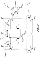
- FIG. 3 illustrates in partial schematic diagram form and partial logic diagram form level converter 60 in accordance with one embodiment of the present invention.
- Level converter 60 includes differential amplifier 61, cross-coupled pull-up circuit 67, NPN transistors 71, 72, 73, and 74, cross-coupled half-latch 75, and output driver portions 81 and 82.
- Differential amplifier 61 includes resistors 62 and 63, NPN transistors 64 and 65, and N-channel transistor 66.
- Cross-coupled half-latch 75 includes NPN transistors 76 and 77 and N-channel transistors 78 and 79.
- Resistor 62 of differential amplifier 61 has a first terminal connected to a regulated power supply voltage terminal labeled "V REG ", and a second terminal.
- Resistor 63 has a first terminal connected to V REG , and a second terminal.
- NPN transistor 64 has a collector connected to the second terminal of resistor 62, a base for receiving buffered signal A, and an emitter.
- NPN transistor 65 has a collector connected to the second terminal of resistor 63, a base for receiving buffered signal A*, and an emitter connected to the emitter of NPN transistor 64.
- N-channel transistor 66 has a drain connected to the emitters of transistors 64 and 65, a gate for receiving bias voltage N BIAS , and a source connected to V SS .
- Cross-coupled pull-up circuit 67 includes P-channel transistors 68 and 69.
- P-channel transistor 68 has a source connected to V REG , a gate connected to the emitter of NPN transistor 73 at node 105, and a drain connected to the second terminal of resistor 63.
- P-channel transistor 69 has a source connected to V REG , a gate connected to the emitter of transistor 74 at node 106, and a drain connected to the second terminal of resistor 62.
- NPN transistor 71 has a collector connected to V DD , a base for receiving a bias voltage labeled "V CLAMP ", and an emitter connected to the second terminal of resistor 62.
- NPN transistor 72 has a collector connected to V DD , a base for receiving bias voltage V CLAMP , and an emitter connected to the second terminal of resistor 63.
- Emitter-follower transistor 73 is an NPN transistor and has a collector connected to V DD , a base connected to the second terminal of resistor 62, and an emitter connected to node 105.
- Emitter-follower transistor 74 is also an NPN transistor and has a collector connected to V DD , a base connected to the second terminal of resistor 63, and an emitter connected to node 106.
- NPN transistor 76 has a base and a collector connected to the emitter of emitter-follower transistor 73 at node 105, and an emitter.
- NPN transistor 77 has a base and a collector connected to the emitter of emitter-follower transistor 74 at node 106, and an emitter.
- NPN transistors 76 and 77 are diode-connected transistors and function as diodes.
- N-channel transistor 78 has a drain connected to the emitter of NPN transistor 76, a gate connected to the collector of NPN transistor 77, and a source connected to V SS .
- N-channel transistor 79 has a drain connected to the emitter of NPN transistor 77, a gate connected to the collector of NPN transistor 76, and a source connected to V SS .
- Output driver portion 81 includes NPN transistor 82, P-channel transistor 83, N-channel transistor 85, and inverter 84.
- NPN transistor 82 has a collector connected to V DD , a base, and an emitter for providing a BINMOS level output signal labeled "A OUT1 ".
- Inverter 84 has an input terminal connected to the emitter of emitter-follower transistor 74 at node 106, and an output terminal connected to the base of NPN transistor 82.
- Inverter 84 is a conventional CMOS inverter.
- P-channel transistor 83 has a source connected to the base of transistor 82, a gate connected to V SS , and a drain connected to the emitter of NPN transistor 82
- N-channel transistor 85 has a drain connected to the emitter of NPN transistor 82, a gate connected to the input terminal of inverter 84 at node 106, and a source connected to V SS .
- Output driver portion 86 includes NPN transistor 87, P-channel transistor 88, N-channel transistor 90, and inverter 89.
- NPN transistor 87 has a collector connected to V DD , a base, and an emitter for providing a BINMOS level output signal labeled "A OUT1 *".
- Inverter 89 has an input terminal connected to the emitter of emitter-follower transistor 73 at node 105, and an output terminal connected to the base of NPN transistor 87.
- Inverter 89 is also be a conventional CMOS inverter.
- P-channel transistor 88 has a source connected to the base of transistor 87, a gate connected to V SS , and a drain connected to the emitter of NPN transistor 87
- N-channel transistor 90 has a drain connected to the emitter of NPN transistor 87, a gate connected to the input terminal of inverter 89 at node 105, and a source connected to V SS .
- level converter 60 receives buffered signals A and A* from input buffer 20 of FIG. 1, and provides BINMOS level output signals A OUT1 and A OUT1 *.
- Buffered signals A and A* are differential signals that swing between a logic high of 1.6 volts and a logic low of 1.0 volt, and are received by NPN transistors 64 and 65 of differential amplifier 61. If buffered signal A is an intermediate logic high and buffered signal A* is an intermediate logic low, then a current designated as I66 through N-channel transistor 66 will be steered through NPN transistor 64 so that the voltage at the base of emitter-follower transistor 73 is reduced low enough to result in emitter-follower transistor 73 becoming substantially non-conductive. The voltage at the base of emitter-follower transistor 74 will be increased to a voltage high enough to cause emitter-follower transistor 74 to be conductive.
- Node 106 will be a logic high voltage equal to approximately V REG minus one V BE .
- N-channel transistor 78 When node 106 is a logic high voltage, and emitter-follower transistor 73 is substantially non-conductive, N-channel transistor 78 is conductive, thus reducing the voltage at node 105 to a logic low voltage.
- node 105 When node 105 is reduced to a logic low voltage of about 0.6 volts, diode-connected NPN transistor 76 becomes substantially non-conductive, causing N-channel transistor 78 to become substantially non-conductive. If N-channel transistor 78 was allowed to remain conductive, current would continue to flow unnecessarily, thus increasing power consumption. Since node 105 is low, the voltage at the gate of N-channel transistor 79 is low enough to cause N-channel transistor 79 to be substantially non-conductive. Also, a low voltage at node 105 causes P-channel transistor 68 of cross-coupled pull-up circuit 67 to become conductive, which helps to increase the voltage at the base of emitter-follower transistor 74 more rapidly.
- buffered signal A is an intermediate logic low and buffered signal A* is an intermediate logic high
- a current designated as I66 through N-channel transistor 66 is steered through NPN transistor 65.
- the voltage at the base of emitter-follower transistor 74 is reduced low enough to result in emitter-follower transistor 74 becoming substantially non-conductive.
- the base of emitter-follower transistor 73 is increased to a voltage high enough to cause emitter-follower transistor 73 to become conductive, and node 105 will be equal to a logic high voltage of V REG minus one V BE .
- N-channel transistor 79 When node 105 is a logic high voltage and emitter follower transistor 74 is non-conductive, N-channel transistor 79 is conductive, thus reducing the voltage at node 106 to a logic low. Since node 106 is low, N-channel transistor 78 is substantially non-conductive. When the voltage at node 106 reduced to a logic low, P-channel transistor 69 becomes conductive, which helps to pull-up the base of NPN transistor 73 more rapidly.
- the gates of P-channel transistors 68 and 69 may be connected to the second terminals of resistors 62 and 63, respectively. This provides a higher voltage to the gates of transistors 68 and 69, thus causing them to be less conductive and reducing the amount of base drive provided to emitter-follower transistors 73 and 74.
- Resistors 62 and 63 are sized relatively large to prevent diode-connected NPN transistors 76 and 77 and N-channel transistors 85 and 90 (in output driver portions 81 and 86) from becoming conductive at high power supply voltages. As the power supply voltage increases, the voltage at nodes 105 and 106 increases. If a logic low voltage at node 105 or 106 increases above about 0.6 voltages, the base-emitter voltage of diode-connected NPN transistors 76 and 77 increases above 0.6 volts, and N-channel transistors 78 and 79 may become at least partially conductive when they should be substantially non-conductive. But, if resistors 62 and 63 are too large, the speed of level converter 60 may be adversely affected.
- differential amplifier 61 and cross-coupled pull-up circuit 67 are provided with regulated power supply voltage V REG .
- Regulating the power supply voltage allows the size of resistors 62 and 63 to be reduced. Resistors 62 and 63 are sized so that the voltage drop across each is equal to approximately 1.7 volts. Also, in the preferred embodiment, regulated power supply voltage V REG is supplied to provide 3.1 volts nominal with less than 50 millivolts of variation. Although a regulated power supply is used in the preferred embodiment, a non-regulated power supply voltage, such as V DD , may be used in other embodiments if resistors 62 and 63 are sized appropriately.
- a clamping circuit comprising NPN transistors 71 and 72 and bias voltage V CLAMP , prevents NPN transistors 64 and 65 from operating in the saturation region.
- a bipolar transistor operates in the saturation region when both the base-emitter and base-collector junctions are forward biased by more than approximately 0.7 volts.
- the base-collector junction of NPN transistors 64 and 65 may become forward biased as a result of several different conditions. For example, if buffered signals A and A* are allowed to increase to a high voltage level as a result of power supply fluctuations, NPN transistors 64 and 65 may operate in saturation.
- NPN transistors 64 and 65 will be reduced enough to cause NPN transistors 64 and 65 to operate in saturation.
- Bias voltage V CLAMP is provided to the bases of NPN transistors 71 and 72 at about 2.1 volts, preventing the collectors of NPN transistors 64 and 65 from going below about 1.3 volts. This causes NPN transistor 64 and 65 to stay in the active region of operation. Operating NPN transistors 64 and 65 in the active region provides the advantage of increased speeds.
- buffered signals A and A* are provided by input buffer 20 (see FIG. 1), and referenced to V SS so that buffered signals A and A* are not affected by variations of V DD .
- Cross-coupled half-latch 75 provides the advantage of reduced power consumption.
- N-channel transistors 78 and 79 are cross-coupled and made conductive only when necessary to reduce the voltage of nodes 105 or 106 to a logic low.
- Diode-connected NPN transistors 76 and 77 further reduce power consumption by preventing a leakage current from flowing and ensuring that N-channel transistors 78 and 79 remain non-conductive during a logic low state.
- Output driver portions 81 and 86 are conventional BICMOS output drivers. Output driver portions 81 and 86 receive the voltages at nodes 106 and 105, respectively, and provide complementary BINMOS level output signals A OUT1 and A OUT1 *. BINMOS level output signal A OUT1 is inverted from the voltage level provided by node 106 and BINMOS level output signal A OUT1 * is inverted from the voltage level provided by node 105.
- NPN transistor 82 functions as a pull-up transistor
- N-channel transistor 85 functions as a pull-down transistor.
- inverter 84 provides a logic high to the base of NPN transistor 82, making NPN transistor 82 conductive.
- N-channel transistor 85 is non-conductive, and output signal A OUT1 is pulled to a logic high voltage approximately equal to V DD minus one V BE (approximately 2.5 volts).
- P-channel transistor 83 helps to prevent excessive reverse-biasing of the base-emitter junction of NPN transistor 82 when the voltage at the base of NPN transistor 82 is reduced to a logic low.
- P-channel transistor 83 eventually increases the voltage of output signal A OUT1 to V DD , eliminating the V BE voltage drop across NPN transistor 82.
- inverter 84 provides a logic low to the base of NPN transistor 82, causing NPN transistor 82 to be substantially non-conductive.
- N-channel transistor 85 becomes conductive, causing output signal A OUT1 to be reduced to a logic low voltage approximately equal to V SS .
- output signal A OUT1 is provided as a logic low
- node 106 is a logic low
- output signal A OUT1 is provided as a logic high.
- Output driver portion 86 is the same as output driver portion 81 and operates in the same manner. Note that output driver portions 81 and 86 are presented as an example of an BICMOS output driver circuit. There are various other BICMOS output drivers circuits that can be substituted for output driver portions 81 and 86.
- FIG. 4 illustrates in partial schematic diagram form and partial logic diagram form level converter 110 in accordance with another embodiment of the present invention.
- Level converter 110 includes operational amplifier 111, cross-coupled half-latch 128, NPN transistors 117, 119, 121, and 122, resistor 118, and output driver portion 130.
- Operational amplifier 111 includes P-channel transistors 112 and 113, NPN transistors 114 and 115, and N-channel transistor 116.
- P-channel transistor 112 has a source connected to V REG , and a gate connected to its drain.
- P-channel transistor 113 has a source connected to V REG , a gate connected to the gate of P-channel transistor 112, and a drain.
- NPN transistor 114 has a collector connected to the drain of P-channel transistor 112, a base for receiving reference voltage V REF , and an emitter.
- NPN transistor 115 has a collector connected to the drain of P-channel transistor 113, a base for receiving single-ended signal A2, and an emitter connected to the emitter of NPN transistor 114.
- N-channel transistor 116 has a drain connected to the emitters of NPN transistors 114 and 115, a gate for receiving bias voltage N BIAS , and a source connected to V SS .
- NPN transistor 117 has a collector connected to V DD a base for receiving bias voltage V CLAMP , and an emitter connected to the collector of NPN transistor 114.
- Resistor 118 has a first terminal connected to V REG , and a second terminal connected to the collector of NPN transistor 114.
- NPN transistor 119 has a collector connected to V DD , a base connected to the base of NPN transistor 117 for receiving bias voltage V CLAMP , and an emitter connected to the collector of NPN transistor 115.
- Emitter-follower transistor 121 has a collector connected to V DD , a base connected to the collector of NPN transistor 114, and an emitter.
- Emitter-follower transistor 122 has a collector connected to V DD , a base connected to the collector of NPN transistor 115, and an emitter.
- Cross-coupled half-latch 128 includes NPN transistors 123 and 124, and N-channel transistors 126 and 127.
- NPN transistor 123 has a base and a collector connected to the emitter of emitter-follower transistor 121, and an emitter.
- NPN transistor 124 has a base and a collector connected to the emitter of emitter-follower transistor 122 at node 107, and an emitter.
- NPN transistors 123 and 124 are therefore diode-connected and perform the function of diodes.
- N-channel transistor 126 has a drain connected to the emitter of NPN transistor 123, a gate connected to the emitter of NPN transistor 122 at node 107, and a source connected to V SS .
- N-channel transistor 127 has a drain connected to the emitter of NPN transistor 124, a gate connected to the emitter of NPN transistor 121, and a source connected V SS .
- Output portion 130 includes NPN transistor 131, P-channel transistor 132, N-channel transistor 134, and inverter 133.
- NPN transistor 131 has a collector connected to V DD , a base, and an emitter for providing a BINMOS output signal labeled "A OUT2 ".
- Inverter 133 has an input terminal connected to the emitter of emitter-follower transistor 122 at node 107, and an output terminal connected to the base of NPN transistor 131.
- P-channel transistor 132 has a source connected to the base of transistor 131, a gate connected to V SS , and a drain connected to the emitter of NPN transistor 131
- N-channel transistor 134 has a drain connected to the emitter of NPN transistor 131, a gate connected to the input terminal of inverter 133 at node 107, and a source connected to V SS .
- level converter 110 receives buffered single-ended signal A2, reference voltage V REF , and provides single-ended BINMOS level output signal A OUT2 .
- Reference voltage V REF is provided to the base of NPN transistor 114 at a level approximately at the midpoint of the logic swing of buffered signal A2.
- P-channel transistors 112 and 113 are connected to form a current mirror, and provide the loads for operational amplifier 111.
- Buffered signal A2 is referenced to V SS and provided at a logic high of about 1.5 volts and a logic low of about 0.9 volts.
- a circuit similar to input buffer 20 of FIG. 1 (not shown) provides buffered signal A2. In other embodiments, other types of input buffers may supply a buffered signal to level converter 110.
- NPN transistor 115 When buffered signal A2 is equal to a logic high, NPN transistor 115 is conductive and NPN transistor 114 is substantially non-conductive. P-channel transistors 112 and 113 are substantially non-conductive. Emitter-follower transistor 122 is substantially non-conductive, and the voltage at node 107 is reduced to about 0.6 volts by cross-coupled half-latch 128.
- Cross-coupled half-latch 128 is the same as cross-coupled half-latch 75 of FIG. 3, which was discussed above.
- NPN transistor 114 When buffered signal A2 is equal to a logic low, NPN transistor 114 is conductive and NPN transistor 115 is substantially non-conductive. P-channel transistors 112 and 113 are conductive, emitter-follower transistor 122 is conductive, and the voltage at node 107 is equal to a logic high voltage approximately equal to V REG minus one V BE .
- a clamping circuit comprising NPN transistors 117 and 119 and bias voltage V CLAMP prevent NPN transistors 114 and 115 from operating in the saturation region, as described above in the discussion of level converter 60 of FIG. 3. Also, output driver portion 130 is the same as output driver portions 81 and 86 of FIG. 3.
- Resistor 118 is sized to help prevent the voltage at the collector of NPN transistor 114 from dropping below about 1.3 volts. This allows P-channel transistor 112 to be reduced in sized, thereby decreasing the junction capacitance of P-channel transistor 112. Reducing the junction capacitance results in an increase in switching speed. Also, emitter-follower transistor 121 may be smaller in size because emitter-follower transistor 121 is not required to drive a load, hence improving the switching speed of level converter 110.
- level converter 60 can be easily adapted to convert from ECL to CMOS logic levels.
- power supply voltage terminal V DD may be connected to ground and power supply voltage terminal V SS may be supplied with a negative power supply voltage. Accordingly, it is intended by the appended claims to cover all modifications of the invention which fall within the true spirit and scope of the invention.
Abstract
Description
- A related, copending application is entitled "Power Supply Dependent Input Buffer", by Hamed Ghassemi et al., attorney docket number SC-01381A, assigned to the assignee hereof, claiming priority from US patent application No. 953,153 and filed concurrently herewith.
- This invention relates generally to logic level conversion, and more particularly, to a BICMOS level converter circuit.
- Integrated circuits are required to operate at increasingly lower power supply voltages and increasingly higher speeds. Integrated circuits are often used in applications where low power consumption and high speed are important, such as in a battery powered computer, or the like. An effective method for decreasing power consumption is to use a lower power supply voltage (for example, 3.3 volts).
- There are several different logic families from which to choose when designing an integrated circuit. Among the different logic families are ECL and BINMOS. ECL (emitter-coupled logic) circuits employ bipolar transistors that operate in the active operating region and typically provide very high switching speeds, however, ECL circuits consume a large amount of power. The difference between an ECL logic high and an ECL logic low is only about one base-emitter diode voltage drop (VBE). On the other hand, a BINMOS logic high is about one VBE below the positive power supply voltage, and a BINMOS logic low is approximately equal to the negative power supply voltage. BINMOS logic is usually implemented using BICMOS technology. A BICMOS circuit combines bipolar transistors with CMOS (complementary metal-oxide-semiconductor) transistors on the same integrated circuit. Generally, the bipolar transistors of a BICMOS circuit provide the advantage of high speed and high drive capability, while the CMOS transistors provide the advantage of reduced power consumption.
- In order to achieve compatibility between the two different logic families, a level conversion circuit converts, or translates, a logic signal from ECL logic levels to BINMOS logic levels. A level conversion circuit should not cause excessive delay or consume a large amount of power. A conventional BICMOS level converter has a differential amplifier, emitter-follower input transistors for receiving an ECL level logic signal, and emitter-follower output transistors. The differential amplifier includes NPN transistors having their emitters coupled together, and a resistor coupled between each of the collectors and a positive power supply voltage terminal. N-channel MOSFET current sources are used to supply a relatively constant current.
- The conventional BICMOS level converter, designed to operate with a power supply voltage of 5.0 volts, may not work reliability with a 3.3 volt power supply. When a 3.3 volt power supply is used instead of the 5.0 volt power supply, the operating margins of some of the transistors in the level converter circuit may be reduced. The margins are reduced in the conventional BICMOS level converter because a VBE voltage drop across a forward biased bipolar transistor is independent of the power supply voltage, and remains relatively constant. Therefore, when the power supply voltage is reduced, there may not be sufficient voltage range to allow for all of the VBE voltage drops without adversely affecting the operation of the circuit. Also, the integrated circuit may be more vulnerable to noise and to fluctuations in power supply voltages. In addition, the conventional BICMOS level converter may be considerably slower when operated at a lower power supply voltage, because the bipolar transistors of the ECL portion of the level converter may now be operating in the saturation operating region. If the bipolar transistors are allowed to operate in saturation, increased switching time, and an undesirable reduction in speed may result.
- Accordingly, there is provided, in one form, a level converter for converting signals operating within a first predetermined voltage level range to a second predetermined voltage level range. The level converter includes a differential amplifier, a first emitter-follower circuit, a second emitter-follower circuit, and cross-coupled half-latch means. The differential amplifier is coupled to a first power supply voltage terminal, and includes first and second resistors and first and second bipolar transistors, and receives first and second input signals within the first predetermined voltage level range. In response, the differential amplifier provides first and second differential signals. The first emitter-follower circuit is coupled to the differential amplifier and receives the first differential signal. In response, the first emitter-follower circuit provides a third signal within the second predetermined voltage level range. The second emitter-follower circuit is coupled to the differential amplifier and receives the second differential signal. In response, the second emitter-follower circuit provides a fourth signal within the second predetermined voltage level range. The cross-coupled half-latch means is coupled to the first and second emitter-follower circuits, and reduces the fourth signal from a high voltage level to a low voltage level within the range of said second predetermined voltage level range in response to a high voltage level being provided by the second emitter-follower circuit. The cross-coupled half-latch also reduces the third signal from a high voltage level to a low voltage level within the range of the second predetermined voltage level range in response to a high voltage level being provided by the first emitter-follower circuit. These and other features and advantages will be more clearly understood from the following detailed description taken in conjunction with the accompanying drawings.
-
- FIG. 1 illustrates in schematic diagram form an input buffer in accordance with the present invention.
- FIG. 2 illustrates in schematic diagram form a power supply dependent bias voltage generator circuit in accordance with the present invention.
- FIG. 3 illustrates in partial schematic diagram form and partial logic diagram form a level converter in accordance with one embodiment of the present invention.
- FIG. 4 illustrates in partial schematic diagram form and partial logic diagram form a level converter in accordance with another embodiment of the present invention.
- FIG. 1 illustrates in schematic diagram form input buffer 20 in accordance with the present invention. Input buffer 20 includes
differential amplifier 22, emitter-follower transistors resistors channel transistors Differential amplifier 22 includesresistors NPN transistors channel transistor 28. -
Resistor 24 ofdifferential amplifier 22 has a first terminal connected to a positive power supply voltage terminal labeled "VDD", and a second terminal connected tonode 101.Resistor 25 has a first terminal connected to VDD, and a second terminal connected tonode 102.NPN transistor 26 has a collector connected to the second terminal ofresistor 24 atnode 101, a base for receiving an ECL level single-ended input signal labeled "AIN", and an emitter.NPN transistor 27 has a collector connected to the second terminal ofresistor 25 atnode 102, a base for receiving a reference voltage labeled "VREF", and emitter connected to the emitter ofNPN transistor 26. N-channel transistor 28 has a drain connected to the emitters ofNPN transistors follower transistor 29 has a collector connected to VDD, a base connected to the second terminal ofresistor 24 atnode 101, and an emitter.Resistor 30 has a first terminal connected to the emitter of emitter-follower transistor 29, and a second terminal for providing a buffered signal labeled "A*". N-channel transistor 31 has a drain connected to the second terminal ofresistor 30, a gate for receiving a power supply dependent bias voltage labeled "CBIAS", and a source connected to VSS. Emitter-follower transistor 32 has a collector connected to VDD, a base connected to the second terminal ofresistor 25 atnode 102, and an emitter.Resistor 33 has a first terminal connected to the emitter of emitter-follower transistor 32, and a second terminal for providing a buffered signal labeled "A". N-channel transistor 34 has a drain connected to the second terminal ofresistor 33, a gate for receiving power supply dependent bias voltage CBIAS, and a source connected to VSS. Note that an asterisk (*) after the signal name indicates that the signal is active at a logic low. - In operation, single-ended ECL level input signal AIN is received by input buffer 20 at the base of
NPN transistor 26. ECL level input signal AIN swings between an ECL logic level high of 1.6 volts and an ECL logic low of about 0.8 volts. N-channel transistor 28 receives bias voltage NBIAS and provides a current source fordifferential amplifier 22. NBIAS is provided at about 1.2 to 1.4 volts. Reference voltage VREF is provided to the base ofNPN transistor 27 at a voltage level approximately at the midpoint of the logic swing of ECL level input signal AIN. If input signal AIN is a logic low, it is more negative than reference voltage VREF,NPN transistor 26 will be substantially non-conductive andNPN transistor 27 will be conductive. A current designated as "I₂₈", through N-channel transistor 28, will be steered throughNPN transistor 27, and the voltage atnode 102 will be equal to VDD minus I₂₈R₂₅ where R₂₅ is the resistance ofresistor 25. The voltage atnode 101 will be equal to approximately VDD since there is substantially no current flow throughNPN transistor 26. If input signal AIN is equal to a logic high voltage, it is less negative than VREF, causingNPN transistor 26 to be conductive andNPN transistor 27 to be substantially non-conductive. Current I₂₈ will be steered throughNPN transistor 26 and the voltage atnode 101 will be equal to VDD minus I₂₈R₂₄ where R₂₄ is the resistance ofresistor 24, and the voltage atnode 102 will be equal to approximately VDD. Therefore, the difference between a logic high and a logic low voltage atnodes differential amplifier 22 is equal to the voltage drop across either ofresistors - Emitter-
follower transistors nodes follower transistor 29 provides a voltage equal to the voltage atnode 101 less one base-emitter diode voltage drop (VBE), where one VBE is equal to approximately 0.8 volts. The emitter oftransistor 32 provides a voltage equal to the voltage atnode 102 less one VBE. Resistors 30 and 33 perform a level shift function by reducing the voltage provided by emitter-follower transistors resistors channel transistors resistors channel transistors channel transistors channel transistors channel transistors resistors resistors channel transistors - As described above, bias voltage CBIAS is chosen so that the drain-source current provided by N-
channel transistors resistors resistors - In the preferred embodiment, buffered signals A and A* swing between a intermediate logic high voltage of 1.6 volts and a logic low voltage of 1.0 volt, and VSS is chosen to be ground. In the preferred embodiment, buffered signals A and A* are provided to
level converter 60 of FIG. 3. Since buffered signals A and A* are referenced to VSS, better margins and increased signal swings inlevel converter 60 are realized. - FIG. 2 illustrates in schematic diagram form, power supply dependent bias
voltage generator circuit 40 in accordance with the present invention. Power supply dependentbias voltage circuit 40 includesresistors operational amplifier 46, N-channel transistors current mirror 52.Operational amplifier 46 includes P-channel transistors 47 and 48,NPN transistors channel transistor 51. P-channel transistors 47 and 48 function as loads foroperational amplifier 46.Current mirror 52 includes P-channel transistors -
Resistor 41 has a first terminal connected to VDD, and a second terminal. N-channel transistor 42 has a drain connected to the second terminal ofresistor 41, a gate for receiving NBIAS, and a source connected to VSS. NPN transistor 44 has a collector connected to VDD, a base connected to the second terminal ofresistor 41, and an emitter connected tonode 103. N-channel transistor 45 has a drain connected to the emitter of NPN transistor 44 atnode 103, a gate for receiving power supply dependent bias voltage CBIAS, and a source connected to VSS. - P-channel transistor 47 of
operational amplifier 46 has a source connected to VDD, a gate, and a drain. P-channel transistor 48 has a source connected to VDD, and a gate and a drain connected to the gate of P-channel transistor 47.NPN transistor 49 has a collector connected to the drain of P-channel transistor 47, a base connected to the emitter of NPN transistor 44 atnode 103, and an emitter.NPN transistor 50 has a collector connected to the drain of P-channel transistor 48, a base connected tonode 104, and an emitter connected to the emitter ofNPN transistor 49. N-channel transistor 51 has a drain connected to the emitters ofNPN transistors - P-
channel transistor 53 ofcurrent mirror 52 has a source connected to VDD, a gate connected to the drain of P-channel transistor 47, and a drain connected to the base ofNPN transistor 50 atnode 104. P-channel transistor 56 has a source connected to VDD, a gate connected to the gate of P-channel transistor 53, and a drain for providing power supply dependent bias voltage CBIAS. Resistor 54 has a first terminal connected to the base oftransistor 50 atnode 104, and a second terminal for receiving a band gap voltage labeled "VBG". N-channel transistor 57 has a gate and a drain connected to the drain of P-channel transistor 56, and a source connected to VSS. - In operation, N-
channel transistor 42 and bias voltage NBIAS provide a relatively constant current source forresistor 41, making the voltage drop acrossresistor 41 relatively constant with respect to VDD. NPN transistor 44 provides a voltage to the base ofNPN transistor 49 atnode 103 approximately equal to the voltage at the second terminal ofresistor 41, less one VBE. Since the voltage drop acrossresistor 41 is relatively constant with respect to VDD, the voltage atnode 103 is also relatively constant with respect to VDD. P-channel transistors 47 and 48 form a current mirror, causing the collector current ofNPN transistor 50 to follow the collector current ofNPN transistor 49. Therefore, the voltage atnode 104 follows the variations of the voltage atnode 103 at approximately the same voltage. Bandgap voltage VBG is a conventional bandgap generated reference voltage and is provided to the second terminal ofresistor 54. A bandgap generated reference voltage is substantially independent of changes in power supply voltage, temperature, and processing. Therefore, the voltage drop acrossresistor 54 varies proportionally to VDD, causing the drain-source current through P-channel transistor 53 to vary as VDD varies. P-channel transistors current mirror 52. As the drain-source current through P-channel transistor 53 changes, the drain-source current through P-channel transistor 56 "mirrors" the change. The gate-to-source voltage of N-channel transistor 57 provides power supply dependent bias voltage CBIAS. N-channel transistor 57 remains in saturation. Therefore, the drain-source current of N-channel transistor 57 changes as VDD changes. If VDD increases, power supply dependent bias voltage CBIAS increases, and if VDD decreases, bias voltage CBIAS decreases. - The characteristics of some integrated circuit devices change with respect to temperature. Power supply dependent bias
voltage generator circuit 40 matches the temperature variations of input buffer 20. NPN transistor 44 of power supply dependentbias voltage circuit 40 tracks the VBE voltage shifts ofNPN transistors transistors channel transistors channel transistor 45 also changes, causing the VBE voltage drop acrossNPN transistor channel transistor 45. In addition,resistor 54 tracks the temperature variations ofresistors - FIG. 3 illustrates in partial schematic diagram form and partial logic diagram
form level converter 60 in accordance with one embodiment of the present invention.Level converter 60 includesdifferential amplifier 61, cross-coupled pull-upcircuit 67,NPN transistors latch 75, andoutput driver portions Differential amplifier 61 includesresistors NPN transistors channel transistor 66. Cross-coupled half-latch 75 includesNPN transistors channel transistors -
Resistor 62 ofdifferential amplifier 61 has a first terminal connected to a regulated power supply voltage terminal labeled "VREG", and a second terminal.Resistor 63 has a first terminal connected to VREG, and a second terminal.NPN transistor 64 has a collector connected to the second terminal ofresistor 62, a base for receiving buffered signal A, and an emitter.NPN transistor 65 has a collector connected to the second terminal ofresistor 63, a base for receiving buffered signal A*, and an emitter connected to the emitter ofNPN transistor 64. N-channel transistor 66 has a drain connected to the emitters oftransistors - Cross-coupled pull-up
circuit 67 includes P-channel transistors channel transistor 68 has a source connected to VREG, a gate connected to the emitter ofNPN transistor 73 atnode 105, and a drain connected to the second terminal ofresistor 63. P-channel transistor 69 has a source connected to VREG, a gate connected to the emitter oftransistor 74 atnode 106, and a drain connected to the second terminal ofresistor 62. -
NPN transistor 71 has a collector connected to VDD, a base for receiving a bias voltage labeled "VCLAMP", and an emitter connected to the second terminal ofresistor 62.NPN transistor 72 has a collector connected to VDD, a base for receiving bias voltage VCLAMP, and an emitter connected to the second terminal ofresistor 63. Emitter-follower transistor 73 is an NPN transistor and has a collector connected to VDD, a base connected to the second terminal ofresistor 62, and an emitter connected tonode 105. Emitter-follower transistor 74 is also an NPN transistor and has a collector connected to VDD, a base connected to the second terminal ofresistor 63, and an emitter connected tonode 106.NPN transistor 76 has a base and a collector connected to the emitter of emitter-follower transistor 73 atnode 105, and an emitter.NPN transistor 77 has a base and a collector connected to the emitter of emitter-follower transistor 74 atnode 106, and an emitter.NPN transistors channel transistor 78 has a drain connected to the emitter ofNPN transistor 76, a gate connected to the collector ofNPN transistor 77, and a source connected to VSS. N-channel transistor 79 has a drain connected to the emitter ofNPN transistor 77, a gate connected to the collector ofNPN transistor 76, and a source connected to VSS. -
Output driver portion 81 includesNPN transistor 82, P-channel transistor 83, N-channel transistor 85, andinverter 84.NPN transistor 82 has a collector connected to VDD, a base, and an emitter for providing a BINMOS level output signal labeled "AOUT1".Inverter 84 has an input terminal connected to the emitter of emitter-follower transistor 74 atnode 106, and an output terminal connected to the base ofNPN transistor 82.Inverter 84 is a conventional CMOS inverter. P-channel transistor 83 has a source connected to the base oftransistor 82, a gate connected to VSS, and a drain connected to the emitter ofNPN transistor 82, N-channel transistor 85 has a drain connected to the emitter ofNPN transistor 82, a gate connected to the input terminal ofinverter 84 atnode 106, and a source connected to VSS. -
Output driver portion 86 includesNPN transistor 87, P-channel transistor 88, N-channel transistor 90, andinverter 89.NPN transistor 87 has a collector connected to VDD, a base, and an emitter for providing a BINMOS level output signal labeled "AOUT1*".Inverter 89 has an input terminal connected to the emitter of emitter-follower transistor 73 atnode 105, and an output terminal connected to the base ofNPN transistor 87.Inverter 89 is also be a conventional CMOS inverter. P-channel transistor 88 has a source connected to the base oftransistor 87, a gate connected to VSS, and a drain connected to the emitter ofNPN transistor 87, N-channel transistor 90 has a drain connected to the emitter ofNPN transistor 87, a gate connected to the input terminal ofinverter 89 atnode 105, and a source connected to VSS. - In operation,
level converter 60 receives buffered signals A and A* from input buffer 20 of FIG. 1, and provides BINMOS level output signals AOUT1 and AOUT1*. Buffered signals A and A* are differential signals that swing between a logic high of 1.6 volts and a logic low of 1.0 volt, and are received byNPN transistors differential amplifier 61. If buffered signal A is an intermediate logic high and buffered signal A* is an intermediate logic low, then a current designated as I₆₆ through N-channel transistor 66 will be steered throughNPN transistor 64 so that the voltage at the base of emitter-follower transistor 73 is reduced low enough to result in emitter-follower transistor 73 becoming substantially non-conductive. The voltage at the base of emitter-follower transistor 74 will be increased to a voltage high enough to cause emitter-follower transistor 74 to be conductive.Node 106 will be a logic high voltage equal to approximately VREG minus one VBE. - When
node 106 is a logic high voltage, and emitter-follower transistor 73 is substantially non-conductive, N-channel transistor 78 is conductive, thus reducing the voltage atnode 105 to a logic low voltage. Whennode 105 is reduced to a logic low voltage of about 0.6 volts, diode-connectedNPN transistor 76 becomes substantially non-conductive, causing N-channel transistor 78 to become substantially non-conductive. If N-channel transistor 78 was allowed to remain conductive, current would continue to flow unnecessarily, thus increasing power consumption. Sincenode 105 is low, the voltage at the gate of N-channel transistor 79 is low enough to cause N-channel transistor 79 to be substantially non-conductive. Also, a low voltage atnode 105 causes P-channel transistor 68 of cross-coupled pull-upcircuit 67 to become conductive, which helps to increase the voltage at the base of emitter-follower transistor 74 more rapidly. - If buffered signal A is an intermediate logic low and buffered signal A* is an intermediate logic high, then a current designated as I₆₆ through N-
channel transistor 66 is steered throughNPN transistor 65. The voltage at the base of emitter-follower transistor 74 is reduced low enough to result in emitter-follower transistor 74 becoming substantially non-conductive. The base of emitter-follower transistor 73 is increased to a voltage high enough to cause emitter-follower transistor 73 to become conductive, andnode 105 will be equal to a logic high voltage of VREG minus one VBE. Whennode 105 is a logic high voltage andemitter follower transistor 74 is non-conductive, N-channel transistor 79 is conductive, thus reducing the voltage atnode 106 to a logic low. Sincenode 106 is low, N-channel transistor 78 is substantially non-conductive. When the voltage atnode 106 reduced to a logic low, P-channel transistor 69 becomes conductive, which helps to pull-up the base ofNPN transistor 73 more rapidly. - In other embodiments, the gates of P-
channel transistors resistors transistors follower transistors -
Resistors NPN transistors channel transistors 85 and 90 (inoutput driver portions 81 and 86) from becoming conductive at high power supply voltages. As the power supply voltage increases, the voltage atnodes node NPN transistors channel transistors resistors level converter 60 may be adversely affected. Therefore, in the preferred embodiment,differential amplifier 61 and cross-coupled pull-upcircuit 67 are provided with regulated power supply voltage VREG. Regulating the power supply voltage allows the size ofresistors Resistors resistors - A clamping circuit, comprising
NPN transistors NPN transistors NPN transistors NPN transistors channel transistor 66 is allowed to vary, the collector voltage ofNPN transistors NPN transistors NPN transistors NPN transistors NPN transistor NPN transistors - Cross-coupled half-
latch 75 provides the advantage of reduced power consumption. N-channel transistors nodes NPN transistors channel transistors -
Output driver portions Output driver portions nodes node 106 and BINMOS level output signal AOUT1* is inverted from the voltage level provided bynode 105. - In
output driver portion 81,NPN transistor 82 functions as a pull-up transistor, and N-channel transistor 85 functions as a pull-down transistor. Whennode 106 is a logic low,inverter 84 provides a logic high to the base ofNPN transistor 82, makingNPN transistor 82 conductive. N-channel transistor 85 is non-conductive, and output signal AOUT1 is pulled to a logic high voltage approximately equal to VDD minus one VBE (approximately 2.5 volts). P-channel transistor 83 helps to prevent excessive reverse-biasing of the base-emitter junction ofNPN transistor 82 when the voltage at the base ofNPN transistor 82 is reduced to a logic low. Also, P-channel transistor 83 eventually increases the voltage of output signal AOUT1 to VDD, eliminating the VBE voltage drop acrossNPN transistor 82. Whennode 106 becomes a logic high,inverter 84 provides a logic low to the base ofNPN transistor 82, causingNPN transistor 82 to be substantially non-conductive. N-channel transistor 85 becomes conductive, causing output signal AOUT1 to be reduced to a logic low voltage approximately equal to VSS. When the voltage atnode 106 is a logic high, output signal AOUT1 is provided as a logic low, and whennode 106 is a logic low, output signal AOUT1 is provided as a logic high.Output driver portion 86 is the same asoutput driver portion 81 and operates in the same manner. Note thatoutput driver portions output driver portions - FIG. 4 illustrates in partial schematic diagram form and partial logic diagram
form level converter 110 in accordance with another embodiment of the present invention.Level converter 110 includesoperational amplifier 111, cross-coupled half-latch 128,NPN transistors resistor 118, andoutput driver portion 130. -
Operational amplifier 111 includes P-channel transistors NPN transistors channel transistor 116. P-channel transistor 112 has a source connected to VREG, and a gate connected to its drain. P-channel transistor 113 has a source connected to VREG, a gate connected to the gate of P-channel transistor 112, and a drain.NPN transistor 114 has a collector connected to the drain of P-channel transistor 112, a base for receiving reference voltage VREF, and an emitter.NPN transistor 115 has a collector connected to the drain of P-channel transistor 113, a base for receiving single-ended signal A₂, and an emitter connected to the emitter ofNPN transistor 114. N-channel transistor 116 has a drain connected to the emitters ofNPN transistors NPN transistor 114.Resistor 118 has a first terminal connected to VREG, and a second terminal connected to the collector ofNPN transistor 114.NPN transistor 119 has a collector connected to VDD, a base connected to the base ofNPN transistor 117 for receiving bias voltage VCLAMP, and an emitter connected to the collector ofNPN transistor 115. Emitter-follower transistor 121 has a collector connected to VDD, a base connected to the collector ofNPN transistor 114, and an emitter. Emitter-follower transistor 122 has a collector connected to VDD, a base connected to the collector ofNPN transistor 115, and an emitter. - Cross-coupled half-
latch 128 includesNPN transistors channel transistors NPN transistor 123 has a base and a collector connected to the emitter of emitter-follower transistor 121, and an emitter.NPN transistor 124 has a base and a collector connected to the emitter of emitter-follower transistor 122 atnode 107, and an emitter.NPN transistors channel transistor 126 has a drain connected to the emitter ofNPN transistor 123, a gate connected to the emitter ofNPN transistor 122 atnode 107, and a source connected to VSS. N-channel transistor 127 has a drain connected to the emitter ofNPN transistor 124, a gate connected to the emitter ofNPN transistor 121, and a source connected VSS. -
Output portion 130 includesNPN transistor 131, P-channel transistor 132, N-channel transistor 134, andinverter 133.NPN transistor 131 has a collector connected to VDD, a base, and an emitter for providing a BINMOS output signal labeled "AOUT2".Inverter 133 has an input terminal connected to the emitter of emitter-follower transistor 122 atnode 107, and an output terminal connected to the base ofNPN transistor 131. P-channel transistor 132 has a source connected to the base oftransistor 131, a gate connected to VSS, and a drain connected to the emitter ofNPN transistor 131, N-channel transistor 134 has a drain connected to the emitter ofNPN transistor 131, a gate connected to the input terminal ofinverter 133 atnode 107, and a source connected to VSS. - In operation,
level converter 110 receives buffered single-ended signal A₂, reference voltage VREF, and provides single-ended BINMOS level output signal AOUT2. Reference voltage VREF is provided to the base ofNPN transistor 114 at a level approximately at the midpoint of the logic swing of buffered signal A₂. P-channel transistors operational amplifier 111. Buffered signal A₂ is referenced to VSS and provided at a logic high of about 1.5 volts and a logic low of about 0.9 volts. A circuit similar to input buffer 20 of FIG. 1 (not shown) provides buffered signal A₂. In other embodiments, other types of input buffers may supply a buffered signal tolevel converter 110. - When buffered signal A₂ is equal to a logic high,
NPN transistor 115 is conductive andNPN transistor 114 is substantially non-conductive. P-channel transistors follower transistor 122 is substantially non-conductive, and the voltage atnode 107 is reduced to about 0.6 volts by cross-coupled half-latch 128. Cross-coupled half-latch 128 is the same as cross-coupled half-latch 75 of FIG. 3, which was discussed above. - When buffered signal A₂ is equal to a logic low,
NPN transistor 114 is conductive andNPN transistor 115 is substantially non-conductive. P-channel transistors follower transistor 122 is conductive, and the voltage atnode 107 is equal to a logic high voltage approximately equal to VREG minus one VBE. A clamping circuit, comprisingNPN transistors NPN transistors level converter 60 of FIG. 3. Also,output driver portion 130 is the same asoutput driver portions -
Resistor 118 is sized to help prevent the voltage at the collector ofNPN transistor 114 from dropping below about 1.3 volts. This allows P-channel transistor 112 to be reduced in sized, thereby decreasing the junction capacitance of P-channel transistor 112. Reducing the junction capacitance results in an increase in switching speed. Also, emitter-follower transistor 121 may be smaller in size because emitter-follower transistor 121 is not required to drive a load, hence improving the switching speed oflevel converter 110. - While the invention has been described in the context of a preferred embodiment, it will be apparent to those skilled in the art that the present invention may be modified in numerous ways and may assume many embodiments other than that specifically set out and described above. For example,
level converter 60 can be easily adapted to convert from ECL to CMOS logic levels. Also, power supply voltage terminal VDD may be connected to ground and power supply voltage terminal VSS may be supplied with a negative power supply voltage. Accordingly, it is intended by the appended claims to cover all modifications of the invention which fall within the true spirit and scope of the invention.
Claims (10)
- A level converter (60) for converting signals operating within a first predetermined voltage level range to a second predetermined voltage level range, the level converter comprising:
a differential amplifier (61), including first and second resistors (62, 63) and first and second bipolar transistors (64, 65), for receiving first and second input signals within said first predetermined voltage level range, and in response providing first and second differential signals, said differential amplifier (61) coupled to a first power supply voltage terminal;
a first emitter-follower circuit (73), coupled to said differential amplifier (61), for receiving said first differential signal, and in response, providing a third signal within said second predetermined voltage level range;
a second emitter-follower circuit (74), coupled to said differential amplifier (61), for receiving said second differential signal, and in response, providing a fourth signal within said second predetermined voltage level range; and
cross-coupled half-latch means (75), coupled to said first and second emitter-follower circuits (73, 74), for reducing said fourth signal from a high voltage level to a low voltage level within the range of said second predetermined voltage level range in response to a high voltage level being provided by said second emitter-follower circuit (74), and for reducing said third signal from a high voltage level to a low voltage level within the range of said second predetermined voltage level range in response to a high voltage level being provided by said first emitter-follower circuit (73). - The level converter (60) of claim 1, further comprising clamping means (71, 72), for preventing said first and second bipolar transistors (64, 65) from operating in a saturation operating region.
- The level converter (60) of claim 1, wherein said first and second resistors (62, 63) are each P-channel transistors.
- A BICMOS level converter circuit (60) for converting signals operating within a first predetermined voltage level range to a second predetermined voltage level range, the level converter (60) comprising:
a differential amplifier (61), including first and second resistors (62, 63) and first and second bipolar transistors (64, 65), for receiving first and second input signals within said first predetermined voltage level range, and in response providing first and second differential signals, said differential amplifier (61) coupled to a first power supply voltage terminal;
a first emitter-follower circuit (73), coupled to said differential amplifier (61), for receiving said first differential signal, and in response, providing a third signal within said second predetermined voltage level range;
a second emitter-follower circuit (74), coupled to said differential amplifier (61), for receiving said second differential signal, and in response, providing a fourth signal within said second predetermined voltage level range;
cross-coupled half-latch (75), coupled to said first and second emitter-follower circuits (73, 74), for reducing said fourth signal from a high voltage level to a low voltage level within the range of said second predetermined voltage level range in response to a high voltage level being provided by said second emitter-follower circuit (74), and for reducing said third signal from a high voltage level to a low voltage level within the range of said second predetermined voltage level range in response to a high voltage level being provided by said first emitter-follower circuit (73);
cross-coupled pull-up means (67), coupled between said first power supply voltage terminal and a first current electrode of said first and second bipolar transistors (64, 65), for increasing the voltage at said first current electrode of said first bipolar transistor (64) in response to a low voltage level being provided by said second emitter-follower circuit (74), and for increasing the voltage at said first current electrode of said second bipolar transistor (65) in response to a low voltage level being provided by said first emitter-follower circuit (73); and
clamping means (71, 72), for preventing said first and second bipolar transistors (64, 65) from operating in a saturation operating region. - The BICMOS level converter circuit (60) of claim 4, wherein said first emitter-follower circuit (73) comprises a third bipolar transistor, and said second emitter-follower circuit comprises a fourth bipolar transistor (74).
- The BICMOS level converter circuit (60) of claim 5, wherein said cross-coupled pull-up means (67) comprises:
a first P-channel transistor (68) having a first current electrode coupled to said first power supply voltage terminal, a second current electrode coupled to said first current electrode of said second bipolar transistor (65), and a control electrode coupled to an emitter of said third bipolar transistor (73); and
a second P-channel transistor (69) having a first current electrode coupled to said first power supply voltage terminal, a second current electrode coupled to said first current electrode of said first bipolar transistor (64), and a control electrode coupled to an emitter of said fourth bipolar transistor (74). - The BICMOS level converter circuit (60) of claim 5, wherein said cross-coupled half-latch means (75) comprises:
a first diode (76) having a first terminal coupled to a second current electrode of said third bipolar transistor (73), and a second terminal;
a first N-channel transistor (78) having a first current electrode coupled to said second terminal of said first diode (76), a control electrode coupled to said second current electrode of said fourth bipolar transistor (74), and a second current electrode coupled to a second power supply voltage terminal;
a second diode (77) having a first terminal coupled to a second current electrode of said fourth bipolar transistor (74), and a second terminal; and
a second N-channel transistor (79) having a first current electrode coupled to said second terminal of said second diode (77), a control electrode coupled to said second current electrode of said third bipolar transistor (73), and a second current electrode coupled to a second power supply voltage terminal. - The BICMOS level converter circuit (61) of claim 4, wherein said first power supply voltage terminal is characterized as providing a regulated power supply voltage.
- The BICMOS level converter circuit (61) of claim 4, wherein said clamping means (71, 72) comprises:
a fifth bipolar transistor (71) having a first current electrode coupled to said first power supply voltage terminal, a control electrode for receiving a bias voltage, and a second current electrode coupled to said first current electrode of said first bipolar transistor (64); and
a sixth bipolar transistor (72) having a first current electrode coupled to said first power supply voltage terminal, a control electrode for receiving a bias voltage, and a second current electrode coupled to said first current electrode of said second bipolar transistor (65). - An ECL to BINMOS level converter (60), comprising:
an input buffer (20) for receiving an ECL level logic signal and providing a first and second differential signals of a predetermined voltage level in response thereto;
differential amplifier means (61), coupled to a first positive power supply voltage terminal, for receiving said first and second differential signals, and having first and second differential outputs for providing third and fourth differential signals;
a first emitter-follower transistor (73) having a collector coupled to a second positive power supply voltage terminal, a base coupled to said first differential output, and an emitter;
a second emitter-follower transistor (74) having a collector coupled to said second positive power supply voltage terminal, a base coupled to said second differential output, and an emitter;
a first P-channel transistor (68) having a source coupled to said first positive power supply voltage terminal, a gate coupled to said emitter of said first emitter-follower transistor (73), and a drain coupled to said second differential output;
a second P-channel transistor (69) having a source coupled to said first positive power supply voltage terminal, a gate coupled to said emitter of said second emitter-follower transistor (74), and a drain coupled to said first differential output;
a first bipolar transistor (76) having a collector and a base coupled to said emitter of said first emitter-follower transistor (73), and an emitter;
a second bipolar transistor (77) having a collector and a base coupled to said emitter of said second emitter-follower transistor (74), and an emitter;
a first N-channel transistor (78) having a drain coupled to said emitter of said first bipolar transistor (76), a gate coupled to said emitter of said second emitter-follower transistor (74), and a source coupled to a negative power supply voltage terminal;
a second N-channel transistor (79) having a drain coupled to said emitter of said second bipolar transistor (77), a gate coupled to said emitter of said first emitter-follower transistor (73), and a source coupled to said negative power supply voltage terminal; and
output driver means (86), coupled to said emitter of said first emitter-follower transistor (73), for providing a BINMOS level output signal.
Priority Applications (1)
| Application Number | Priority Date | Filing Date | Title |
|---|---|---|---|
| EP97108906A EP0794620A3 (en) | 1992-09-28 | 1993-07-02 | Power supply dependent input buffer |
Applications Claiming Priority (2)
| Application Number | Priority Date | Filing Date | Title |
|---|---|---|---|
| US07/951,959 US5315179A (en) | 1992-09-28 | 1992-09-28 | BICMOS level converter circuit |
| US951959 | 1992-09-28 |
Related Child Applications (1)
| Application Number | Title | Priority Date | Filing Date |
|---|---|---|---|
| EP97108906.5 Division-Into | 1997-06-03 |
Publications (3)
| Publication Number | Publication Date |
|---|---|
| EP0590247A2 true EP0590247A2 (en) | 1994-04-06 |
| EP0590247A3 EP0590247A3 (en) | 1994-04-27 |
| EP0590247B1 EP0590247B1 (en) | 1997-12-29 |
Family
ID=25492392
Family Applications (2)
| Application Number | Title | Priority Date | Filing Date |
|---|---|---|---|
| EP97108906A Withdrawn EP0794620A3 (en) | 1992-09-28 | 1993-07-02 | Power supply dependent input buffer |
| EP93110587A Expired - Lifetime EP0590247B1 (en) | 1992-09-28 | 1993-07-02 | BICMOS level converter circuit |
Family Applications Before (1)
| Application Number | Title | Priority Date | Filing Date |
|---|---|---|---|
| EP97108906A Withdrawn EP0794620A3 (en) | 1992-09-28 | 1993-07-02 | Power supply dependent input buffer |
Country Status (5)
| Country | Link |
|---|---|
| US (1) | US5315179A (en) |
| EP (2) | EP0794620A3 (en) |
| JP (1) | JPH06204845A (en) |
| KR (1) | KR940008261A (en) |
| DE (1) | DE69315937T2 (en) |
Cited By (3)
| Publication number | Priority date | Publication date | Assignee | Title |
|---|---|---|---|---|
| EP0642226A2 (en) * | 1993-09-08 | 1995-03-08 | Advanced Micro Devices, Inc. | Translator circuits with symmetrical switching delays |
| CN108886355A (en) * | 2016-03-31 | 2018-11-23 | 高通股份有限公司 | Highly efficient power voltage level shifter circuit |
| WO2023143230A1 (en) * | 2022-01-27 | 2023-08-03 | 深圳市九天睿芯科技有限公司 | Signal amplification circuit |
Families Citing this family (9)
| Publication number | Priority date | Publication date | Assignee | Title |
|---|---|---|---|---|
| IT1236879B (en) * | 1989-11-22 | 1993-04-26 | Sgs Thomson Microelectronics | COMPARATOR ELECTRONIC CIRCUIT |
| US5485106A (en) * | 1994-04-05 | 1996-01-16 | Sun Microsystems, Inc. | ECL to CMOS converter |
| US5446400A (en) * | 1994-11-07 | 1995-08-29 | Motorola Inc. | GTL compatible BICMOS input stage |
| US5502405A (en) * | 1994-11-08 | 1996-03-26 | Cypress Semiconductor Corporation | Method and apparatus for CML/EC to CMOS/TTL translators |
| US5675809A (en) * | 1995-02-10 | 1997-10-07 | Ncr Corporation | Voltage control circuit for a dual voltage bus computer system |
| US6600338B1 (en) * | 2001-05-04 | 2003-07-29 | Rambus, Inc. | Apparatus and method for level-shifting input receiver circuit from high external voltage to low internal supply voltage |
| US6801080B1 (en) * | 2003-04-07 | 2004-10-05 | Pericom Semiconductor Corp. | CMOS differential input buffer with source-follower input clamps |
| US7352229B1 (en) * | 2006-07-10 | 2008-04-01 | Altera Corporation | Reference clock receiver compliant with LVPECL, LVDS and PCI-Express supporting both AC coupling and DC coupling |
| US7595660B2 (en) * | 2007-08-16 | 2009-09-29 | Texas Instruments Incorporated | Low-delay complimentary metal-oxide semiconductor (CMOS) to emitter-coupled logic (ECL) converters, methods and apparatus |
Citations (2)
| Publication number | Priority date | Publication date | Assignee | Title |
|---|---|---|---|---|
| US5059829A (en) * | 1990-09-04 | 1991-10-22 | Motorola, Inc. | Logic level shifting circuit with minimal delay |
| US5148059A (en) * | 1991-04-02 | 1992-09-15 | International Business Machines Corporation | CMOS and ECL logic circuit requiring no interface circuitry |
Family Cites Families (14)
| Publication number | Priority date | Publication date | Assignee | Title |
|---|---|---|---|---|
| US4527078A (en) * | 1982-08-23 | 1985-07-02 | Signetics Corporation | Signal translator with supply voltage compensation particularly for use as interface between current tree logic and transistor-transistor logic |
| JPS59219007A (en) * | 1983-05-27 | 1984-12-10 | Hitachi Ltd | Mos amplifier circuit |
| JPS61269525A (en) * | 1985-05-24 | 1986-11-28 | Nec Corp | Current switching type logic circuit |
| US4644194A (en) * | 1985-06-24 | 1987-02-17 | Motorola, Inc. | ECL to TTL voltage level translator |
| GB2209104A (en) * | 1987-08-26 | 1989-04-26 | Philips Nv | An amplifier load circuit and an amplifier including the load circuit |
| US4849659A (en) * | 1987-12-15 | 1989-07-18 | North American Philips Corporation, Signetics Division | Emitter-coupled logic circuit with three-state capability |
| US4806799A (en) * | 1988-02-26 | 1989-02-21 | Motorola, Inc. | ECL to CMOS translator |
| DE58908391D1 (en) * | 1988-07-22 | 1994-10-27 | Siemens Ag | ECL-CMOS converter. |
| JPH0777346B2 (en) * | 1988-12-28 | 1995-08-16 | 株式会社東芝 | Logic level conversion circuit |
| US4988898A (en) * | 1989-05-15 | 1991-01-29 | National Semiconductor Corporation | High speed ECL/CML to TTL translator circuit |
| US5013941A (en) * | 1989-08-17 | 1991-05-07 | National Semiconductor Corporation | TTL to ECL/CML translator circuit |
| US5216298A (en) * | 1989-12-14 | 1993-06-01 | Mitsubishi Denki Kabushiki Kaisha | ECL input buffer for BiCMOS |
| US5068551A (en) * | 1990-09-21 | 1991-11-26 | National Semiconductor Corporation | Apparatus and method for translating ECL signals to CMOS signals |
| US5148061A (en) * | 1991-02-27 | 1992-09-15 | Motorola, Inc. | ECL to CMOS translation and latch logic circuit |
-
1992
- 1992-09-28 US US07/951,959 patent/US5315179A/en not_active Expired - Fee Related
-
1993
- 1993-07-02 DE DE69315937T patent/DE69315937T2/en not_active Expired - Fee Related
- 1993-07-02 EP EP97108906A patent/EP0794620A3/en not_active Withdrawn
- 1993-07-02 EP EP93110587A patent/EP0590247B1/en not_active Expired - Lifetime
- 1993-09-22 KR KR1019930019279A patent/KR940008261A/en not_active Application Discontinuation
- 1993-09-22 JP JP5259196A patent/JPH06204845A/en active Pending
Patent Citations (2)
| Publication number | Priority date | Publication date | Assignee | Title |
|---|---|---|---|---|
| US5059829A (en) * | 1990-09-04 | 1991-10-22 | Motorola, Inc. | Logic level shifting circuit with minimal delay |
| US5148059A (en) * | 1991-04-02 | 1992-09-15 | International Business Machines Corporation | CMOS and ECL logic circuit requiring no interface circuitry |
Non-Patent Citations (2)
| Title |
|---|
| IBM TECHNICAL DISCLOSURE BULLETIN. vol. 14, no. 12 , May 1972 , NEW YORK US pages 3684 - 3685 LANE 'bipolar fet high -speed logic switch' * |
| RESEARCH DISCLOSURE no. 310 , February 1990 , HAVANT GB page 141 'current switch circuit with vpnp pull-up and load device' * |
Cited By (5)
| Publication number | Priority date | Publication date | Assignee | Title |
|---|---|---|---|---|
| EP0642226A2 (en) * | 1993-09-08 | 1995-03-08 | Advanced Micro Devices, Inc. | Translator circuits with symmetrical switching delays |
| EP0642226A3 (en) * | 1993-09-08 | 1995-09-06 | Advanced Micro Devices Inc | Translator circuits with symmetrical switching delays. |
| CN108886355A (en) * | 2016-03-31 | 2018-11-23 | 高通股份有限公司 | Highly efficient power voltage level shifter circuit |
| US11223359B2 (en) | 2016-03-31 | 2022-01-11 | Qualcomm Incorporated | Power efficient voltage level translator circuit |
| WO2023143230A1 (en) * | 2022-01-27 | 2023-08-03 | 深圳市九天睿芯科技有限公司 | Signal amplification circuit |
Also Published As
| Publication number | Publication date |
|---|---|
| EP0590247A3 (en) | 1994-04-27 |
| JPH06204845A (en) | 1994-07-22 |
| DE69315937T2 (en) | 1998-06-18 |
| US5315179A (en) | 1994-05-24 |
| EP0590247B1 (en) | 1997-12-29 |
| DE69315937D1 (en) | 1998-02-05 |
| EP0794620A2 (en) | 1997-09-10 |
| EP0794620A3 (en) | 1997-10-29 |
| KR940008261A (en) | 1994-04-29 |
Similar Documents
| Publication | Publication Date | Title |
|---|---|---|
| US4501978A (en) | Level shift interface circuit | |
| US4703203A (en) | BICMOS logic having three state output | |
| US5315179A (en) | BICMOS level converter circuit | |
| US5309039A (en) | Power supply dependent input buffer | |
| US4804868A (en) | BiMOS logical circuit | |
| US6281731B1 (en) | Control of hysteresis characteristic within a CMOS differential receiver | |
| US5469097A (en) | Translator circuit with symmetrical switching delays | |
| US5015888A (en) | Circuit and method of generating logic output signals from an ECL gate to drive a non-ECL gate | |
| US5202594A (en) | Low power level converter | |
| US6114874A (en) | Complementary MOS level translating apparatus and method | |
| US5331225A (en) | BiCMOS logic circuit with bipolar transistor and MOS transistor formed on the same semiconductor substrate | |
| US5075578A (en) | Input buffer regenerative latch | |
| US4868904A (en) | Complementary noise-immune logic | |
| US5446400A (en) | GTL compatible BICMOS input stage | |
| US5113095A (en) | BiCMOS logic circuit with a CML output | |
| JP2557996B2 (en) | Complementary emitta follower driver | |
| US5999017A (en) | CMOS implemented output buffer circuit for providing ECL level signals | |
| JP2544826B2 (en) | Semiconductor integrated circuit | |
| EP0630109B1 (en) | Low-voltage output driving circuit | |
| EP0433685B1 (en) | Semiconductor integrated circuit having ECL circuits | |
| JP2953005B2 (en) | Bi-CMOS circuit | |
| US5229658A (en) | Switching circuit | |
| US5434517A (en) | ECL output buffer with a MOS transistor used for tristate enable | |
| EP0476341B1 (en) | A BICMOS logic circuit with a CML output | |
| US6211660B1 (en) | MOS transistor output circuits using PMOS transistors |
Legal Events
| Date | Code | Title | Description |
|---|---|---|---|
| PUAI | Public reference made under article 153(3) epc to a published international application that has entered the european phase |
Free format text: ORIGINAL CODE: 0009012 |
|
| PUAL | Search report despatched |
Free format text: ORIGINAL CODE: 0009013 |
|
| AK | Designated contracting states |
Kind code of ref document: A2 Designated state(s): DE FR GB IT |
|
| AK | Designated contracting states |
Kind code of ref document: A3 Designated state(s): DE FR GB IT |
|
| 17P | Request for examination filed |
Effective date: 19941027 |
|
| 17Q | First examination report despatched |
Effective date: 19960604 |
|
| GRAG | Despatch of communication of intention to grant |
Free format text: ORIGINAL CODE: EPIDOS AGRA |
|
| GRAG | Despatch of communication of intention to grant |
Free format text: ORIGINAL CODE: EPIDOS AGRA |
|
| GRAH | Despatch of communication of intention to grant a patent |
Free format text: ORIGINAL CODE: EPIDOS IGRA |
|
| GRAH | Despatch of communication of intention to grant a patent |
Free format text: ORIGINAL CODE: EPIDOS IGRA |
|
| GRAA | (expected) grant |
Free format text: ORIGINAL CODE: 0009210 |
|
| AK | Designated contracting states |
Kind code of ref document: B1 Designated state(s): DE FR GB IT |
|
| XX | Miscellaneous (additional remarks) |
Free format text: TEILANMELDUNG 97108906.5 EINGEREICHT AM 03/06/97. |
|
| ITF | It: translation for a ep patent filed |
Owner name: BARZANO' E ZANARDO ROMA S.P.A. |
|
| REF | Corresponds to: |
Ref document number: 69315937 Country of ref document: DE Date of ref document: 19980205 |
|
| ET | Fr: translation filed | ||
| PGFP | Annual fee paid to national office [announced via postgrant information from national office to epo] |
Ref country code: GB Payment date: 19980630 Year of fee payment: 6 |
|
| PGFP | Annual fee paid to national office [announced via postgrant information from national office to epo] |
Ref country code: FR Payment date: 19980707 Year of fee payment: 6 |
|
| PGFP | Annual fee paid to national office [announced via postgrant information from national office to epo] |
Ref country code: DE Payment date: 19980727 Year of fee payment: 6 |
|
| PLBE | No opposition filed within time limit |
Free format text: ORIGINAL CODE: 0009261 |
|
| STAA | Information on the status of an ep patent application or granted ep patent |
Free format text: STATUS: NO OPPOSITION FILED WITHIN TIME LIMIT |
|
| 26N | No opposition filed | ||
| PG25 | Lapsed in a contracting state [announced via postgrant information from national office to epo] |
Ref country code: GB Free format text: LAPSE BECAUSE OF NON-PAYMENT OF DUE FEES Effective date: 19990702 |
|
| PG25 | Lapsed in a contracting state [announced via postgrant information from national office to epo] |
Ref country code: FR Free format text: THE PATENT HAS BEEN ANNULLED BY A DECISION OF A NATIONAL AUTHORITY Effective date: 19990731 |
|
| GBPC | Gb: european patent ceased through non-payment of renewal fee |
Effective date: 19990702 |
|
| PG25 | Lapsed in a contracting state [announced via postgrant information from national office to epo] |
Ref country code: DE Free format text: LAPSE BECAUSE OF NON-PAYMENT OF DUE FEES Effective date: 20000503 |
|
| REG | Reference to a national code |
Ref country code: FR Ref legal event code: ST |
|
| PG25 | Lapsed in a contracting state [announced via postgrant information from national office to epo] |
Ref country code: IT Free format text: LAPSE BECAUSE OF NON-PAYMENT OF DUE FEES;WARNING: LAPSES OF ITALIAN PATENTS WITH EFFECTIVE DATE BEFORE 2007 MAY HAVE OCCURRED AT ANY TIME BEFORE 2007. THE CORRECT EFFECTIVE DATE MAY BE DIFFERENT FROM THE ONE RECORDED. Effective date: 20050702 |