EP0642226A2 - Translator circuits with symmetrical switching delays - Google Patents
Translator circuits with symmetrical switching delays Download PDFInfo
- Publication number
- EP0642226A2 EP0642226A2 EP94305927A EP94305927A EP0642226A2 EP 0642226 A2 EP0642226 A2 EP 0642226A2 EP 94305927 A EP94305927 A EP 94305927A EP 94305927 A EP94305927 A EP 94305927A EP 0642226 A2 EP0642226 A2 EP 0642226A2
- Authority
- EP
- European Patent Office
- Prior art keywords
- signal line
- coupled
- transistor
- voltage
- signal
- Prior art date
- Legal status (The legal status is an assumption and is not a legal conclusion. Google has not performed a legal analysis and makes no representation as to the accuracy of the status listed.)
- Withdrawn
Links
Images


Classifications
-
- H—ELECTRICITY
- H03—ELECTRONIC CIRCUITRY
- H03K—PULSE TECHNIQUE
- H03K19/00—Logic circuits, i.e. having at least two inputs acting on one output; Inverting circuits
- H03K19/02—Logic circuits, i.e. having at least two inputs acting on one output; Inverting circuits using specified components
- H03K19/08—Logic circuits, i.e. having at least two inputs acting on one output; Inverting circuits using specified components using semiconductor devices
- H03K19/082—Logic circuits, i.e. having at least two inputs acting on one output; Inverting circuits using specified components using semiconductor devices using bipolar transistors
- H03K19/086—Emitter coupled logic
-
- H—ELECTRICITY
- H03—ELECTRONIC CIRCUITRY
- H03K—PULSE TECHNIQUE
- H03K19/00—Logic circuits, i.e. having at least two inputs acting on one output; Inverting circuits
- H03K19/0175—Coupling arrangements; Interface arrangements
- H03K19/0185—Coupling arrangements; Interface arrangements using field effect transistors only
- H03K19/018507—Interface arrangements
- H03K19/018521—Interface arrangements of complementary type, e.g. CMOS
- H03K19/018528—Interface arrangements of complementary type, e.g. CMOS with at least one differential stage
-
- H—ELECTRICITY
- H03—ELECTRONIC CIRCUITRY
- H03K—PULSE TECHNIQUE
- H03K19/00—Logic circuits, i.e. having at least two inputs acting on one output; Inverting circuits
- H03K19/003—Modifications for increasing the reliability for protection
- H03K19/00369—Modifications for compensating variations of temperature, supply voltage or other physical parameters
- H03K19/00384—Modifications for compensating variations of temperature, supply voltage or other physical parameters in field effect transistor circuits
Definitions
- This invention relates generally to logic interface and translator circuits and more particularly to ECLto CMOS translators.
- various types of digital logic circuits are used in different parts of the processing system.
- the various circuit types operate at different switching speeds and are used to provide optimal performance for the processing system.
- ECL emitter coupled logic
- CMOS complementary metal-oxide semiconductor
- a translation is often required from one circuit type to another circuit type, because the circuit types operate with different input/output voltages corresponding to high and low logic levels.
- Bipolar ECL voltage levels have a relatively small voltage swing of only about 0.8 volts.
- CMOS voltage levels have a larger voltage swing of about 5.0 volts. Since many of the processing systems are designed with both ECL and CMOS logic circuits, there are interface circuits required, such as ECL to CMOS translator circuits, to allow these two different types of circuits to communicate to each other. For example, ECL to CMOS translators are used to shift the voltage levels of the ECL input logic signals to voltage levels which can be recognized by the CMOS logic circuits.
- the conventional translators do not provide a CMOS output that symmetrically tracks an ECL input. For example, it is desirable that the delay between the ECL signal rise and the CMOS signal rise be equal to the delay between the ECL signal fall and the CMOS signal fall.
- the designs of conventional ECL to CMOS translators do not provide this symmetrical tracking of the signal rise and fall.
- the delays between the ECL input signal transitions and the CMOS output signal transitions are often not symmetrical.
- the fall to fall delay between the ECL input and the CMOS output may be less than the rise to rise delay between the ECL input and the CMOS output due to the difference in voltage levels required for switching between logic levels.
- the difference between fall to fall delay and rise to rise delay can be greater than 1 nanosecond (ns). To provide a symmetrical delay, the difference between the fall to fall delay and rise to rise delay should be .3 ns or less.
- ECL input signal is in the form of ECL differential input signals which are used to carry both data information and the clock frequency of a system, such as a non-return-to-zero, invert-to-one (NRZI) or data/frequency signal
- NRZI non-return-to-zero, invert-to-one
- the lack of symmetry in the CMOS output signal caused by the translator will result in inaccurate detection of the clock frequency.
- the need in the art is addressed by a circuit for providing symmetrical switching delays for differential amplifier including a first signal line and a second signal line complementary to the first signal line and for use with a power line.
- the circuit to be described herein includes a first voltage, clamp coupled to the first signal line and to the power voltage line for limiting a voltage differential between the power voltage line and the first signal line.
- a second voltage clamp is coupled to the power voltage line and the second signal line for limiting a voltage differential between the power voltage line and the second signal line.
- the circuit further includes a third voltage clamp coupled to the first signal line and to the second signal line for limiting a voltage differential between the first signal line and the second signal line.
- first signal line and the second signal line are complementary metal-oxide semiconductor compatible.
- first and second voltage clamps each further include a first transistor having a drain and a gate coupled to the power voltage line and a second transistor having a drain and a gate coupled to a source of the first transistor and a source coupled to the first signal line.
- the third voltage clamp further includes a first pair of p-n diodes coupled in series between the first signal line and the second signal line for limiting the voltage differential between the first and the second signal lines.
- a second pair of p-n diodes is coupled in series between the second signal line and the first signal line for limiting the voltage differential between the second and the first signal lines.
- a translator circuit for generating an output signal which is complementary metal-oxide semiconductor compatible for a differential amplifier responsive to differential input emitter coupled logic signals for generating a first signal and a second signal complementary to the first signal.
- the translator circuit includes a first voltage clamp coupled to a upper power voltage and to the first signal for limiting a voltage differential between the upper power voltage and the first signal.
- a second voltage clamp is coupled to the upper power voltage and to the second signal for limiting a voltage differential between the upper power voltage and the second signal.
- the translator circuit further comprises a third voltage clamp coupled to the first signal line and to the second signal line for limiting a voltage differential therebetween.
- the circuit provides reduced sensitivity to variations in process parameters, power supply voltages, temperature and manufacturing tolerances.
- the circuit also provides symmetrical tracking between the rise to rise and the fall to fall delays.
- the present invention relates to an improvement in a translator circuit.
- the following description is presented to enable one of ordinary skill in the art to make and use the invention as provided in the context of a particular application and its requirements.
- Various modifications to the preferred embodiments will be readily apparent to those skilled in the art, and the generic principles defined here may be applied to other embodiments.
- the present invention is not intended to be limited to the embodiments shown, but is to be accorded the widest scope consistent with the principles and novel features disclosed herein.
- Fig. 1 is an illustrative diagram of a conventional ECL to CMOS translator circuit 10 implemented with CMOS transistors.
- the circuit has a differential input comprising the ECL input positive Vp 12 and the ECL input negative V n 14. These input signals determine the state of the circuit node 16 and the circuit node 18, respectively.
- the circuit node 16 is the input to the gate of the transistor 20 and the circuit node 18 is the input to the gate of the transistor 22.
- the transistor 20 amplifies the signal and the source of the transistor 20 is connected to the circuit node 24.
- the circuit node 24 is the input to the gate of the transistor 26 and the drain of the transistor 26 is coupled to the transistor 28, whose source is the CMOS output 34.
- the circuit has a number of shortcomings.
- the first shortcoming is the inoperability of the circuit when both of the differential ECL inputs are at a lower than normal voltage, which can occur if the ECL inputs are at a low common mode voltage. If the ECL input positive Vp 12 and the ECL input negative V n 14 are both below the threshold of transistors 11 and 14, respectively, then both transistors 11 and 14 will be “ON” and both transistors 20 and 22 will be turned “ON", which is a faulty state of the circuit.
- the second shortcoming is that during normal operation, the circuit node 24 swings from the power V dd 30 to the ground V ss 32, which are nominally 5 volts and 0 volts, respectively.
- the threshold voltage of the transistor 26 is 1 volt.
- To turn the transistor 26 "ON” the circuit node 24 must only transition between 0 to 1 volt, but to turn the transistor 26 “OFF” the circuit node 24 must transition between 5 to 1 volts. Since the slew rate of circuit node 24 is essentially constant over the transition range, the switching of the transistor 26 is not symmetrical, because switching the transistor 26 "ON” is much faster than switching the transistor 26 "OFF". In a similar manner the switching of the transistor 28 is not symmetrical, because switching the transistor 28 "OFF” is faster than switching the transistor 28 "ON”.
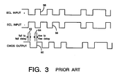
- Fig. 3 The lack of symmetrical switching is illustrated in Fig. 3. As shown the delays between the ECL positive input 56 and the ECL negative input 58, and the CMOS output 60 are not symmetrical. In particular, the fall to fall delay 62 is much shorter in this example than the rise to rise delay 64.
- the third shortcoming of the ECL to CMOS translator circuit 10 is that if the high voltage of either the circuit node 16 or the circuit node 18 are equal to the power V dd 30 minus 1 volts, then the transistor 20 or the transistor 22, respectively, will not turn “OFF” completely. This will result in the transistors turning “ON” fast, but slowly turning “OFF”. This characteristic contributes to unsymmetrical switching delays.
- Fig. 2 is an illustrative diagram of a conventional ECL to CMOS input buffer 40 implemented with bipolar and CMOS transistors.
- the input is the ECL signal input 42, which is amplified through the differential amplifier 43 and the transistor 45 and the transistor 47. These transistors drive an ECL to MOS level shifter, which includes the transistor 49.
- the output is the CMOS output signal 50.
- the shortcoming of the ECL to CMOS input buffer 40 is that the voltages at the signal 44 and the signal 46 are dependent on any variations in the power voltage V cc 41.
- the signal 48 is also dependent on any variations in the power voltage V cc 41.
- the signal 48 transitions through a large voltage swing from the power voltage V cc 41 to the ground 52, which is a 5 volt swing. This results in an unsymmetrical rise to rise and fall to fall switching of the circuit in the manner illustrated in Fig. 3.
- the conventional ECL to CMOS translator circuits do not provide symmetrical rise to rise and fall to fall switching delays between the ECL input signals and the CMOS output signal.
- the present ECL to CMOS translators are also too sensitive to variations in process parameters, power supply voltages, temperature and manufacturing tolerances.
- Fig. 4 is an illustrative diagram of an ECL to CMOS translator circuit 70 with symmetrical rise to rise and fall to fall delays according to the present invention.
- the ECL positive input 72 and the ECL negative input 76 are the inputs to the gates of the transistor 74 and the transistor 78, respectively. These two transistors down convert the ECL inputs by a Vg s level, which is the voltage difference between the gate and the source of a CMOS transistor.
- the transistor 74 source and the transistor 78 source are the inputs to the transistor 80 gates and the transistor 82 gates, respectively.
- Transistors 80 and 82 form a differential amplifier.
- the drain of the transistor 80 is connected to the circuit node 96 and the drain of the transistor 82 is connected to the circuit node 98.
- the circuit node 96 is also connected to the source of the p channel transistor 100 and the gate 106 of the p channel transistor 102.
- the circuit node 98 is connected to the source of the p channel transistor 102 and the gate 104 of the p channel transistor 100.
- a key objective of the ECL to CMOS translator 70 of the present invention is to achieve symmetrical rise to rise and fall to fall delays.
- voltage clamps are implemented between the circuit node 96 and the power voltage V cc 94 and between the circuit node 98 and the power voltage V cc 94, which keep the circuit node 96 and the circuit node 98 from falling below the power voltage V cc 94 minus 2*Vg s volts (V cc -2*V gs ).
- Vg s is the voltage between a gate and a source of a CMOS transistor.
- the voltage clamps are implemented by the transistor 116 and the transistor 118 between the power voltage V cc 94 and the circuit node 96, and by the transistor 120 and the transistor 122 between the power voltage V cc 94 and the circuit node 98.
- the voltage swing of the circuit node 96 and the circuit node 98 is limited to a small range of between the power voltage V cc 94 and the power voltage V cc 94 minus 2*V gs (V cc -2*V gs ).
- the circuit node 96 Without the voltage clamps the circuit node 96, forex- ample, would transition between the power voltage V cc 94 and the ground 92, or about 0 to 5 volts.
- a smaller voltage swing is much less sensitive to variations in process parameters, power supply voltages, temperature and manufacturing tolerances than a large voltage swing.
- a smaller voltage swing also results in a symmetrical rise to rise and fall to fall delay between the ECL signal input and the CMOS output.
- the ECL to CMOS translator 70 has another device to further limit the voltage swing, which is a voltage clamp to limit the voltage difference between the circuit node 96 and the circuit node 98.
- This voltage clamp is implemented by the p-n diode 108 and the p-n diode 110 between the circuit node 98 and the circuit node 96, and the p-n diode 112 and the p-n diode 114 between the circuit node 96 and the circuit node 98.
- this additional voltage clamp is that the circuit node 96 and the circuit node 98 vary between a low voltage of the power voltage V cc 94 minus 2 * Vg s (V cc - 2 * Vg s ) and a high voltage of the power voltage V cc 94 minus 2*V gs plus 2 * Vp n (V cc - 2*V gs + 2 * Vp n ).
- the Vp n voltage is the voltage drop across a p-n diode and, as explained, the Vg s voltage is the voltage drop from a gate to a source of a CMOS transistor.
- the voltage Vg s is about 1 volt and for a diode the voltage Vp n is about .8 volts.
- the circuit node 96 controls the gate of the p channel transistor 126, whose source is coupled to the CMOS output signal 140.
- the circuit node 98 is coupled to the gate of the p channel transistor 124.
- the source of the p channel transistor 124 is connected to the drain of the p channel transistor 128.
- the source of the p channel transistor 128 is connected to the gate and drain of the transistor 130.
- a series of p channel transistors 132, 134, 135, and 136 are connected from the power voltage V cc 94 to the source of the p channel transistor 128.
- the p channel transistor 128 is always “ON”, because its gate is tied to the ground 92.
- the transistor 130 turns “ON” and the p channel transistor 128 provides a resistive load between the p channel transistor 124 and the transistor 130.
- the p channel transistor 124 is "OFF”, then the transistor 130 is “OFF”; however, the trickle current through the series of p channel transistors 132, 134, 135, and 136 keep the transistor 130 slightly “ON”. The effect is to have virtually no signal delay through the p channel transistor 128.
- the source of the p channel transistor 124 is coupled directly to the gate of the transistor 138, whose drain is coupled to the CMOS output signal 140.
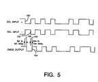
- Fig. 5 is an illustrative timing diagram of the relationship between the ECL input signal and a CMOS output signal for the ECL to CMOS translator 70 with symmetrical rise to rise and fall to fall delays according to the present invention. As shown the delays between the ECL positive input 150 and the ECL negative input 152, and the CMOS output 154 are symmetrical. In particular, the fall to fall delay 156 is equal to the rise to rise delay 158.
- the circuit of the present invention provides reduced sensitivity to variations in process parameters, power supply voltages, temperature and manufacturing tolerances.
- the circuit also provides symmetrical tracking between the rise to rise and the fall to fall delays. Computer simulations have shown that the difference between the rise to rise delay and the fall to fall delay is less than .3 ns.
Abstract
Description
- This invention relates generally to logic interface and translator circuits and more particularly to ECLto CMOS translators.
- In the area of computer data processing systems, various types of digital logic circuits are used in different parts of the processing system. The various circuit types operate at different switching speeds and are used to provide optimal performance for the processing system. In order to transfer data from one part of the processing system having logic of one circuit type (e.g. emitter coupled logic (ECL)) to another part of the processing system having logic of another circuit type (e.g. complementary metal-oxide semiconductor (CMOS)), a translation is often required from one circuit type to another circuit type, because the circuit types operate with different input/output voltages corresponding to high and low logic levels.
- Bipolar ECL voltage levels have a relatively small voltage swing of only about 0.8 volts. CMOS voltage levels have a larger voltage swing of about 5.0 volts. Since many of the processing systems are designed with both ECL and CMOS logic circuits, there are interface circuits required, such as ECL to CMOS translator circuits, to allow these two different types of circuits to communicate to each other. For example, ECL to CMOS translators are used to shift the voltage levels of the ECL input logic signals to voltage levels which can be recognized by the CMOS logic circuits.
- The conventional translators do not provide a CMOS output that symmetrically tracks an ECL input. For example, it is desirable that the delay between the ECL signal rise and the CMOS signal rise be equal to the delay between the ECL signal fall and the CMOS signal fall. The designs of conventional ECL to CMOS translators do not provide this symmetrical tracking of the signal rise and fall. The delays between the ECL input signal transitions and the CMOS output signal transitions are often not symmetrical. For example, the fall to fall delay between the ECL input and the CMOS output may be less than the rise to rise delay between the ECL input and the CMOS output due to the difference in voltage levels required for switching between logic levels. In typical prior translators, the difference between fall to fall delay and rise to rise delay can be greater than 1 nanosecond (ns). To provide a symmetrical delay, the difference between the fall to fall delay and rise to rise delay should be .3 ns or less.
- In addition, conventional translators are sensitive to variations in process parameters, powersupplyvol- tages, temperature and manufacturing tolerances. This sensitivity can significantly affect the symmetrical tracking of signal rise and fall.
- In many applications it is not necessary that there be a symmetrical tracking of the rise and fall. However, when the ECL input signal is in the form of ECL differential input signals which are used to carry both data information and the clock frequency of a system, such as a non-return-to-zero, invert-to-one (NRZI) or data/frequency signal, the lack of symmetry in the CMOS output signal caused by the translator will result in inaccurate detection of the clock frequency.
- Accordingly, there is a need in the art for a circuit that provides reduced sensitivity to variations in process parameters, power supply voltages, temperature and manufacturing tolerances. There is also a need in the art for a circuit that provides symmetrical tracking between the rise to rise and the fall to fall delays.
- The need in the art is addressed by a circuit for providing symmetrical switching delays for differential amplifier including a first signal line and a second signal line complementary to the first signal line and for use with a power line. The circuit to be described herein includes a first voltage, clamp coupled to the first signal line and to the power voltage line for limiting a voltage differential between the power voltage line and the first signal line. A second voltage clamp is coupled to the power voltage line and the second signal line for limiting a voltage differential between the power voltage line and the second signal line.
- In a specific embodiment the circuit further includes a third voltage clamp coupled to the first signal line and to the second signal line for limiting a voltage differential between the first signal line and the second signal line.
- In another specific embodiment the first signal line and the second signal line are complementary metal-oxide semiconductor compatible.
- In another specific embodiment the first and second voltage clamps each further include a first transistor having a drain and a gate coupled to the power voltage line and a second transistor having a drain and a gate coupled to a source of the first transistor and a source coupled to the first signal line.
- In another specific embodiment the third voltage clamp further includes a first pair of p-n diodes coupled in series between the first signal line and the second signal line for limiting the voltage differential between the first and the second signal lines. A second pair of p-n diodes is coupled in series between the second signal line and the first signal line for limiting the voltage differential between the second and the first signal lines.
- In another specific embodiment a translator circuit for generating an output signal is provided which is complementary metal-oxide semiconductor compatible for a differential amplifier responsive to differential input emitter coupled logic signals for generating a first signal and a second signal complementary to the first signal. The translator circuit includes a first voltage clamp coupled to a upper power voltage and to the first signal for limiting a voltage differential between the upper power voltage and the first signal. A second voltage clamp is coupled to the upper power voltage and to the second signal for limiting a voltage differential between the upper power voltage and the second signal.
- In another specific embodiment the translator circuit further comprises a third voltage clamp coupled to the first signal line and to the second signal line for limiting a voltage differential therebetween.
- The circuit provides reduced sensitivity to variations in process parameters, power supply voltages, temperature and manufacturing tolerances. The circuit also provides symmetrical tracking between the rise to rise and the fall to fall delays.
- In the accompanying drawings, by way of example only:
- Fig. 1 is an illustrative diagram of a conventional ECL to CMOS translator circuit implemented with CMOS transistors.
- Fig. 2 is an illustrative diagram of a conventional ECL to CMOS translator circuit implemented with bipolar and CMOS transistors.
- Fig. 3 is an illustrative timing diagram of the relationship between an ECL input signal and a CMOS output signal for a conventional ECL to CMOS translator.
- Fig. 4 is an illustrative diagram of an ECL to CMOS translator circuit with symmetrical rise to rise and fall to fall delays according to the present invention.
- Fig. 5 is an illustrative timing diagram of the relationship between an ECL input signal and a CMOS output signal for an ECL to CMOS translator with symmetrical rise to rise and fall to fall delays according to the present invention.
- The present invention relates to an improvement in a translator circuit. The following description is presented to enable one of ordinary skill in the art to make and use the invention as provided in the context of a particular application and its requirements. Various modifications to the preferred embodiments will be readily apparent to those skilled in the art, and the generic principles defined here may be applied to other embodiments. Thus, the present invention is not intended to be limited to the embodiments shown, but is to be accorded the widest scope consistent with the principles and novel features disclosed herein.
- Fig. 1 is an illustrative diagram of a conventional ECL to
CMOS translator circuit 10 implemented with CMOS transistors. The circuit has a differential input comprising the ECL inputpositive Vp 12 and the ECL inputnegative V n 14. These input signals determine the state of thecircuit node 16 and thecircuit node 18, respectively. Thecircuit node 16 is the input to the gate of thetransistor 20 and thecircuit node 18 is the input to the gate of thetransistor 22. Thetransistor 20 amplifies the signal and the source of thetransistor 20 is connected to thecircuit node 24. Thecircuit node 24 is the input to the gate of thetransistor 26 and the drain of thetransistor 26 is coupled to thetransistor 28, whose source is theCMOS output 34. - This circuit has a number of shortcomings. The first shortcoming is the inoperability of the circuit when both of the differential ECL inputs are at a lower than normal voltage, which can occur if the ECL inputs are at a low common mode voltage. If the ECL input
positive Vp 12 and the ECL inputnegative V n 14 are both below the threshold oftransistors transistors transistors - The second shortcoming is that during normal operation, the
circuit node 24 swings from thepower V dd 30 to theground V ss 32, which are nominally 5 volts and 0 volts, respectively. However, the threshold voltage of thetransistor 26 is 1 volt. To turn thetransistor 26 "ON" thecircuit node 24 must only transition between 0 to 1 volt, but to turn thetransistor 26 "OFF" thecircuit node 24 must transition between 5 to 1 volts. Since the slew rate ofcircuit node 24 is essentially constant over the transition range, the switching of thetransistor 26 is not symmetrical, because switching thetransistor 26 "ON" is much faster than switching thetransistor 26 "OFF". In a similar manner the switching of thetransistor 28 is not symmetrical, because switching thetransistor 28 "OFF" is faster than switching thetransistor 28 "ON". - The lack of symmetrical switching is illustrated in Fig. 3. As shown the delays between the ECL
positive input 56 and the ECLnegative input 58, and theCMOS output 60 are not symmetrical. In particular, the fall to falldelay 62 is much shorter in this example than the rise to risedelay 64. - The third shortcoming of the ECL to
CMOS translator circuit 10 is that if the high voltage of either thecircuit node 16 or thecircuit node 18 are equal to thepower V dd 30 minus 1 volts, then thetransistor 20 or thetransistor 22, respectively, will not turn "OFF" completely. This will result in the transistors turning "ON" fast, but slowly turning "OFF". This characteristic contributes to unsymmetrical switching delays. - Fig. 2 is an illustrative diagram of a conventional ECL to CMOS
input buffer 40 implemented with bipolar and CMOS transistors. In this circuit the input is theECL signal input 42, which is amplified through thedifferential amplifier 43 and thetransistor 45 and thetransistor 47. These transistors drive an ECL to MOS level shifter, which includes the transistor 49. The output is theCMOS output signal 50. - The shortcoming of the ECL to CMOS
input buffer 40 is that the voltages at thesignal 44 and thesignal 46 are dependent on any variations in the power voltage V cc 41. Thesignal 48 is also dependent on any variations in the power voltage Vcc 41. Thesignal 48 transitions through a large voltage swing from the power voltage Vcc 41 to theground 52, which is a 5 volt swing. This results in an unsymmetrical rise to rise and fall to fall switching of the circuit in the manner illustrated in Fig. 3. - In summary the conventional ECL to CMOS translator circuits do not provide symmetrical rise to rise and fall to fall switching delays between the ECL input signals and the CMOS output signal. The present ECL to CMOS translators are also too sensitive to variations in process parameters, power supply voltages, temperature and manufacturing tolerances.
- Fig. 4 is an illustrative diagram of an ECL to CMOS
translator circuit 70 with symmetrical rise to rise and fall to fall delays according to the present invention. The ECLpositive input 72 and the ECLnegative input 76 are the inputs to the gates of thetransistor 74 and thetransistor 78, respectively. These two transistors down convert the ECL inputs by a Vgs level, which is the voltage difference between the gate and the source of a CMOS transistor. Thetransistor 74 source and thetransistor 78 source are the inputs to thetransistor 80 gates and thetransistor 82 gates, respectively.Transistors transistors transistor 78 source, thetransistor 74 source, and thetransistors - The drain of the
transistor 80 is connected to the circuit node 96 and the drain of thetransistor 82 is connected to thecircuit node 98. The circuit node 96 is also connected to the source of thep channel transistor 100 and thegate 106 of thep channel transistor 102. Similarly, thecircuit node 98 is connected to the source of thep channel transistor 102 and thegate 104 of thep channel transistor 100. - In operation, when the
transistor 80 is turned "ON", then the circuit node 96 is pulled low and thep channel transistor 102 is turned "ON". This pulls thecircuit node 98 to thepower voltage V cc 94, which turns thep channel transistor 100 "OFF". Because the ECL signal input is differential, when thetransistor 80 is "ON", thetransistor 82 is "OFF", which also sends thecircuit node 98 to thepower voltage V cc 94, turning thep channel transistor 100 "OFF". - A key objective of the ECL to CMOS
translator 70 of the present invention is to achieve symmetrical rise to rise and fall to fall delays. To achieve this characteristic, voltage clamps are implemented between the circuit node 96 and thepower voltage V cc 94 and between thecircuit node 98 and thepower voltage V cc 94, which keep the circuit node 96 and thecircuit node 98 from falling below thepower voltage V cc 94 minus 2*Vgs volts (Vcc-2*Vgs). As discussed previously, the voltage Vgs is the voltage between a gate and a source of a CMOS transistor. The voltage clamps are implemented by thetransistor 116 and thetransistor 118 between thepower voltage V cc 94 and the circuit node 96, and by thetransistor 120 and thetransistor 122 between thepower voltage V cc 94 and thecircuit node 98. By limiting the low state of the circuit node 96 and thecircuit node 98, the voltage swing of the circuit node 96 and thecircuit node 98 is limited to a small range of between thepower voltage V cc 94 and thepower voltage V cc 94 minus 2*Vgs(Vcc-2*Vgs). Without the voltage clamps the circuit node 96, forex- ample, would transition between thepower voltage V cc 94 and theground 92, or about 0 to 5 volts. A smaller voltage swing is much less sensitive to variations in process parameters, power supply voltages, temperature and manufacturing tolerances than a large voltage swing. A smaller voltage swing also results in a symmetrical rise to rise and fall to fall delay between the ECL signal input and the CMOS output. - The ECL to CMOS
translator 70 has another device to further limit the voltage swing, which is a voltage clamp to limit the voltage difference between the circuit node 96 and thecircuit node 98. This voltage clamp is implemented by thep-n diode 108 and the p-n diode 110 between thecircuit node 98 and the circuit node 96, and the p-n diode 112 and the p-n diode 114 between the circuit node 96 and thecircuit node 98. The effect of this additional voltage clamp is that the circuit node 96 and thecircuit node 98 vary between a low voltage of thepower voltage V cc 94 minus 2*Vgs (Vcc- 2*Vgs) and a high voltage of thepower voltage V cc 94 minus 2*Vgs plus 2*Vpn (Vcc - 2*V gs + 2*Vpn). The Vpn voltage is the voltage drop across a p-n diode and, as explained, the Vgs voltage is the voltage drop from a gate to a source of a CMOS transistor. By further limiting the voltage swing of the circuit node 96 and thecircuit node 98, the sensitivity to power voltage levels and other parameters is reduced and the symmetry of the rise and fall delays is increased. - For a CMOS transistor the voltage Vgs is about 1 volt and for a diode the voltage Vpn is about .8 volts. For a power voltage Vcc of 5 volts, the high voltage of circuit node 96, for example, is (5-2*1+2*.8) = 4.6 volts and the low voltage of circuit node 96 is (5-2*1) = 3 volts. Therefore the voltage difference for the high and low voltages of circuit node 96 is 1.6 volts or about a third of the normal CMOS swing of 5 volts.
- The circuit node 96 controls the gate of the
p channel transistor 126, whose source is coupled to theCMOS output signal 140. Thecircuit node 98 is coupled to the gate of thep channel transistor 124. The source of thep channel transistor 124 is connected to the drain of thep channel transistor 128. The source of thep channel transistor 128 is connected to the gate and drain of thetransistor 130. A series ofp channel transistors power voltage V cc 94 to the source of thep channel transistor 128. These p channel transistors, which are always "ON" because their gates are tied to theground 92, provide a trickle current to keep thetransistor 130 slightly turned "ON". Similarly, thep channel transistor 128 is always "ON", because its gate is tied to theground 92. When thep channel transistor 124 is "ON", then thetransistor 130 turns "ON" and thep channel transistor 128 provides a resistive load between thep channel transistor 124 and thetransistor 130. When thep channel transistor 124 is "OFF", then thetransistor 130 is "OFF"; however, the trickle current through the series ofp channel transistors transistor 130 slightly "ON". The effect is to have virtually no signal delay through thep channel transistor 128. Also, the source of thep channel transistor 124 is coupled directly to the gate of thetransistor 138, whose drain is coupled to theCMOS output signal 140. - Fig. 5 is an illustrative timing diagram of the relationship between the ECL input signal and a CMOS output signal for the ECL to CMOS
translator 70 with symmetrical rise to rise and fall to fall delays according to the present invention. As shown the delays between the ECLpositive input 150 and the ECLnegative input 152, and theCMOS output 154 are symmetrical. In particular, the fall to falldelay 156 is equal to the rise to risedelay 158. - The circuit of the present invention provides reduced sensitivity to variations in process parameters, power supply voltages, temperature and manufacturing tolerances. The circuit also provides symmetrical tracking between the rise to rise and the fall to fall delays. Computer simulations have shown that the difference between the rise to rise delay and the fall to fall delay is less than .3 ns.
- Thus, the present invention has been described herein with reference to a particular embodiment for a particular application. Nonetheless, those having ordinary skill in the art and access to present teachings will recognize additional modifications, applications, and embodiments within the scope thereof. For example, the power supply voltages of the present invention may be replaced by other power supply voltages without departing from the scope of the present invention.
- It is therefore intended by the appended claims to cover any and all such applications, modifications and embodiments within the scope of the present invention.
Claims (20)
Applications Claiming Priority (2)
| Application Number | Priority Date | Filing Date | Title |
|---|---|---|---|
| US11806793A | 1993-09-08 | 1993-09-08 | |
| US118067 | 1993-09-08 |
Publications (2)
| Publication Number | Publication Date |
|---|---|
| EP0642226A2 true EP0642226A2 (en) | 1995-03-08 |
| EP0642226A3 EP0642226A3 (en) | 1995-09-06 |
Family
ID=22376340
Family Applications (1)
| Application Number | Title | Priority Date | Filing Date |
|---|---|---|---|
| EP94305927A Withdrawn EP0642226A3 (en) | 1993-09-08 | 1994-08-10 | Translator circuits with symmetrical switching delays. |
Country Status (5)
| Country | Link |
|---|---|
| US (1) | US5469097A (en) |
| EP (1) | EP0642226A3 (en) |
| JP (1) | JPH07170163A (en) |
| KR (1) | KR950010367A (en) |
| TW (1) | TW307064B (en) |
Cited By (2)
| Publication number | Priority date | Publication date | Assignee | Title |
|---|---|---|---|---|
| EP0788234A3 (en) * | 1996-01-31 | 1997-12-17 | Nec Corporation | ECL to MOS level conversion circuit using CMOS technologies |
| EP0875996A1 (en) * | 1997-04-30 | 1998-11-04 | Phoenix VLSI Consultants Ltd. | Logic device |
Families Citing this family (12)
| Publication number | Priority date | Publication date | Assignee | Title |
|---|---|---|---|---|
| DE69718080T2 (en) * | 1996-01-24 | 2003-10-30 | Mitsubishi Materials Corp | Paving stone for cleaning NOx |
| KR970069274A (en) * | 1996-04-18 | 1997-11-07 | 황선두 | Far-infrared radiation resin mortar composition |
| KR100266876B1 (en) * | 1997-01-24 | 2000-09-15 | 서정숙 | Porous concrete |
| KR100241719B1 (en) * | 1997-01-24 | 2000-02-01 | 김록상 | Bubble porous concrete |
| KR100242599B1 (en) * | 1997-01-24 | 2000-02-01 | 최순호 | High porous concrete |
| KR100248892B1 (en) * | 1997-07-23 | 2000-03-15 | 정숭렬 | Stone mastic asphalt and paving method |
| CA2233527C (en) * | 1998-03-30 | 2002-01-22 | Mitel Semiconductor Ab | Pulse amplifier with low-duty cycle errors |
| US6020762A (en) * | 1998-06-26 | 2000-02-01 | Micron Technology, Inc. | Digital voltage translator and its method of operation |
| US6617895B2 (en) * | 2001-03-30 | 2003-09-09 | Intel Corporation | Method and device for symmetrical slew rate calibration |
| US6535017B1 (en) * | 2001-12-20 | 2003-03-18 | Honeywell International Inc. | CMOS ECL input buffer |
| US7893730B2 (en) * | 2008-07-29 | 2011-02-22 | Silicon Mitus, Inc. | Level shifter and driving circuit including the same |
| KR20190094054A (en) | 2018-02-02 | 2019-08-12 | 황현석 | Pallet manufacturing method using waste plate and pallet manufactured by the same |
Citations (5)
| Publication number | Priority date | Publication date | Assignee | Title |
|---|---|---|---|---|
| EP0154501A2 (en) * | 1984-02-29 | 1985-09-11 | Fujitsu Limited | Logic circuit |
| JPS6372207A (en) * | 1986-09-13 | 1988-04-01 | Fujitsu Ltd | Differential circuit |
| US5059829A (en) * | 1990-09-04 | 1991-10-22 | Motorola, Inc. | Logic level shifting circuit with minimal delay |
| EP0492906A2 (en) * | 1990-12-20 | 1992-07-01 | Sun Microsystems, Inc. | Method and apparatus for high-speed bi-CMOS differential amplifier with controlled output voltage swing |
| EP0590247A2 (en) * | 1992-09-28 | 1994-04-06 | Motorola, Inc. | BICMOS level converter circuit |
Family Cites Families (9)
| Publication number | Priority date | Publication date | Assignee | Title |
|---|---|---|---|---|
| GB1277089A (en) * | 1969-05-23 | 1972-06-07 | Mullard Ltd | Interface transmitter |
| US4499609A (en) * | 1980-08-27 | 1985-02-12 | International Telephone And Telegraph Corporation | Symmetrically clamped fiber optic receiver |
| JPH0773205B2 (en) * | 1983-12-20 | 1995-08-02 | 株式会社日立製作所 | Level conversion circuit |
| US4647799A (en) * | 1984-06-29 | 1987-03-03 | Advanced Micro Devices, Inc. | Full and fractional swing with adjustable high level ECL gate using a single current source |
| US4849659A (en) * | 1987-12-15 | 1989-07-18 | North American Philips Corporation, Signetics Division | Emitter-coupled logic circuit with three-state capability |
| US4812676A (en) * | 1987-12-21 | 1989-03-14 | Digital Equipment Corporation | Current mode logic switching circuit having a Schmitt trigger |
| US5248909A (en) * | 1990-01-09 | 1993-09-28 | Fujitsu Limited | ECL-TO-GaAs level converting circuit |
| US5148061A (en) * | 1991-02-27 | 1992-09-15 | Motorola, Inc. | ECL to CMOS translation and latch logic circuit |
| US5283482A (en) * | 1992-07-06 | 1994-02-01 | Ncr Corporation | CMOS circuit for receiving ECL signals |
-
1994
- 1994-03-19 TW TW083102398A patent/TW307064B/zh active
- 1994-08-10 EP EP94305927A patent/EP0642226A3/en not_active Withdrawn
- 1994-09-06 KR KR1019940022391A patent/KR950010367A/en not_active Application Discontinuation
- 1994-09-07 JP JP6213544A patent/JPH07170163A/en not_active Withdrawn
-
1995
- 1995-05-10 US US08/438,456 patent/US5469097A/en not_active Expired - Fee Related
Patent Citations (5)
| Publication number | Priority date | Publication date | Assignee | Title |
|---|---|---|---|---|
| EP0154501A2 (en) * | 1984-02-29 | 1985-09-11 | Fujitsu Limited | Logic circuit |
| JPS6372207A (en) * | 1986-09-13 | 1988-04-01 | Fujitsu Ltd | Differential circuit |
| US5059829A (en) * | 1990-09-04 | 1991-10-22 | Motorola, Inc. | Logic level shifting circuit with minimal delay |
| EP0492906A2 (en) * | 1990-12-20 | 1992-07-01 | Sun Microsystems, Inc. | Method and apparatus for high-speed bi-CMOS differential amplifier with controlled output voltage swing |
| EP0590247A2 (en) * | 1992-09-28 | 1994-04-06 | Motorola, Inc. | BICMOS level converter circuit |
Non-Patent Citations (1)
| Title |
|---|
| PATENT ABSTRACTS OF JAPAN vol. 12, no. 304 (E-646) 18 August 1988 & JP-A-63 072 207 (FUJITSU LTD) 1 April 1988 * |
Cited By (3)
| Publication number | Priority date | Publication date | Assignee | Title |
|---|---|---|---|---|
| EP0788234A3 (en) * | 1996-01-31 | 1997-12-17 | Nec Corporation | ECL to MOS level conversion circuit using CMOS technologies |
| EP0875996A1 (en) * | 1997-04-30 | 1998-11-04 | Phoenix VLSI Consultants Ltd. | Logic device |
| US6121793A (en) * | 1997-04-30 | 2000-09-19 | Phoenix Vlsi Consultants Ltd. | Logic device |
Also Published As
| Publication number | Publication date |
|---|---|
| TW307064B (en) | 1997-06-01 |
| KR950010367A (en) | 1995-04-28 |
| EP0642226A3 (en) | 1995-09-06 |
| JPH07170163A (en) | 1995-07-04 |
| US5469097A (en) | 1995-11-21 |
Similar Documents
| Publication | Publication Date | Title |
|---|---|---|
| US5206544A (en) | CMOS off-chip driver with reduced signal swing and reduced power supply disturbance | |
| CA1206535A (en) | Interface circuit | |
| US5115150A (en) | Low power CMOS bus receiver with small setup time | |
| US6194920B1 (en) | Semiconductor circuit | |
| KR940003809B1 (en) | Ttl to cmos input buffer | |
| US5113098A (en) | Glitch remover circuit for transmission links | |
| US5469097A (en) | Translator circuit with symmetrical switching delays | |
| KR20010049227A (en) | Level adjustment circuit and data output circuit thereof | |
| JPH041440B2 (en) | ||
| US5278467A (en) | Self-biasing input stage for high-speed low-voltage communication | |
| JPS62194729A (en) | Digital switching circuit | |
| US5994744A (en) | Analog switching circuit | |
| US5239211A (en) | Output buffer circuit | |
| KR100197998B1 (en) | Low power loss input buffer of semiconductor device | |
| KR19990044240A (en) | Output buffer with shared intermediate node | |
| US4943740A (en) | Ultra fast logic | |
| EP0590247B1 (en) | BICMOS level converter circuit | |
| US5432463A (en) | High speed NOR gate with small output voltage swings | |
| US5864245A (en) | Output circuit with overvoltage protection | |
| US5075578A (en) | Input buffer regenerative latch | |
| EP0529545B1 (en) | Level shifting CMOS integrated circuits | |
| US5729156A (en) | ECL to CMOS level translator using delayed feedback for high speed BiCMOS applications | |
| JPH08172348A (en) | Output buffer circuit | |
| JP3175683B2 (en) | Output buffer circuit | |
| JP2798602B2 (en) | Output interface circuit |
Legal Events
| Date | Code | Title | Description |
|---|---|---|---|
| PUAI | Public reference made under article 153(3) epc to a published international application that has entered the european phase |
Free format text: ORIGINAL CODE: 0009012 |
|
| AK | Designated contracting states |
Kind code of ref document: A2 Designated state(s): BE DE DK ES FR GB GR IE IT LU NL PT SE |
|
| PUAL | Search report despatched |
Free format text: ORIGINAL CODE: 0009013 |
|
| AK | Designated contracting states |
Kind code of ref document: A3 Designated state(s): BE DE DK ES FR GB GR IE IT LU NL PT SE |
|
| 17P | Request for examination filed |
Effective date: 19960207 |
|
| 17Q | First examination report despatched |
Effective date: 19970307 |
|
| GRAG | Despatch of communication of intention to grant |
Free format text: ORIGINAL CODE: EPIDOS AGRA |
|
| GRAG | Despatch of communication of intention to grant |
Free format text: ORIGINAL CODE: EPIDOS AGRA |
|
| GRAH | Despatch of communication of intention to grant a patent |
Free format text: ORIGINAL CODE: EPIDOS IGRA |
|
| STAA | Information on the status of an ep patent application or granted ep patent |
Free format text: STATUS: THE APPLICATION IS DEEMED TO BE WITHDRAWN |
|
| 18D | Application deemed to be withdrawn |
Effective date: 19980512 |