US7352229B1 - Reference clock receiver compliant with LVPECL, LVDS and PCI-Express supporting both AC coupling and DC coupling - Google Patents
Reference clock receiver compliant with LVPECL, LVDS and PCI-Express supporting both AC coupling and DC coupling Download PDFInfo
- Publication number
- US7352229B1 US7352229B1 US11/484,366 US48436606A US7352229B1 US 7352229 B1 US7352229 B1 US 7352229B1 US 48436606 A US48436606 A US 48436606A US 7352229 B1 US7352229 B1 US 7352229B1
- Authority
- US
- United States
- Prior art keywords
- pair
- supply voltage
- transistors
- differential
- outputs
- Prior art date
- Legal status (The legal status is an assumption and is not a legal conclusion. Google has not performed a legal analysis and makes no representation as to the accuracy of the status listed.)
- Expired - Fee Related
Links
Images


Classifications
-
- H—ELECTRICITY
- H03—ELECTRONIC CIRCUITRY
- H03K—PULSE TECHNIQUE
- H03K3/00—Circuits for generating electric pulses; Monostable, bistable or multistable circuits
- H03K3/02—Generators characterised by the type of circuit or by the means used for producing pulses
- H03K3/353—Generators characterised by the type of circuit or by the means used for producing pulses by the use, as active elements, of field-effect transistors with internal or external positive feedback
- H03K3/356—Bistable circuits
- H03K3/356104—Bistable circuits using complementary field-effect transistors
- H03K3/356113—Bistable circuits using complementary field-effect transistors using additional transistors in the input circuit
- H03K3/35613—Bistable circuits using complementary field-effect transistors using additional transistors in the input circuit the input circuit having a differential configuration
-
- H—ELECTRICITY
- H04—ELECTRIC COMMUNICATION TECHNIQUE
- H04L—TRANSMISSION OF DIGITAL INFORMATION, e.g. TELEGRAPHIC COMMUNICATION
- H04L25/00—Baseband systems
- H04L25/02—Details ; arrangements for supplying electrical power along data transmission lines
- H04L25/0264—Arrangements for coupling to transmission lines
- H04L25/0272—Arrangements for coupling to multiple lines, e.g. for differential transmission
-
- H—ELECTRICITY
- H04—ELECTRIC COMMUNICATION TECHNIQUE
- H04L—TRANSMISSION OF DIGITAL INFORMATION, e.g. TELEGRAPHIC COMMUNICATION
- H04L25/00—Baseband systems
- H04L25/02—Details ; arrangements for supplying electrical power along data transmission lines
- H04L25/0264—Arrangements for coupling to transmission lines
- H04L25/0292—Arrangements specific to the receiver end
- H04L25/0294—Provision for current-mode coupling
Definitions
- This invention relates to reference clock receivers for use with Programmable Logic Devices (PCDs) or any other suitable electronic device.
- PCDs Programmable Logic Devices
- Clock multiplier phase-lock loops (PLL) in transceivers usually require a “clean” reference clock that is generated from an external crystal clock source.
- FIG. 1 shows a circuit that shows a conventional reference clock receiver structure 100 .
- Reference clock receiver structure 100 includes input buffer 102 , level shift 104 , and CMOS buffer 106 .
- the first stage input buffer 102 is a differential pair of transistors to receive differential inputs (IP and IN).
- the differential pair consists of thick oxide 3.3 volts devices to withstand higher voltage levels seen at the input of the structure.
- the second stage is basically a level shift stage 104 and provides sufficient gain to increase signal swing.
- the third stage 106 further boosts the input signal to provide CMOS level outputs. Duty-cycle connection of the signal is performed in this stage to reduce jitters.
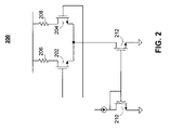
- the lower end of input common mode range is limited to Vgs transistor 202/transistor 204 +VdSAT transistor 212 .
- Resistors 206 and 208 also are used with the differential pair and transistor 210 forms a current mirror together with transistor 212 .
- NMOS differential pair 202 and 204 should be formed from thick oxide. As such, this NMOS-based differential pair's lowest common-mode voltage is sub-optimal because thick oxide devices have larger threshold voltages. In such circumstances, input common-mode voltage could be relatively very high (e.g., above 1 volt).
- This conventional structure may not be able to meet specifications of certain new industry standards such as PCI-Express, whose reference clocks have a common-mode range from 0.25 volts to 0.55 volts.
- receiver clock structure that includes a differential pair formed from relatively thick oxide structures while still being able to accommodate a relatively wide input common-mode range.
- a method of converting an external clock signal source in the form of a differential pair into a reference clock signal includes receiving the pair of differential inputs and buffering the pair of differential outputs using a plurality of transistors of a first oxide thickness to produce a pair of differential pair of outputs. Then, the method preferably requires level shifting the buffered pair of differential outputs using a plurality of transistors of a second oxide thickness, wherein the second oxide thickness is less than the first oxide thickness, in order to provide gain to the differential outputs to form a gained pair of differential outputs. Then the method includes boosting the gained pair of differential outputs and converting the boosted pair of differential outputs into a single signal.
- the method may also include boosting the pair of differential outputs using a plurality of transistors having a third oxide thickness.
- the third oxide thickness is preferably less than the second oxide thickness.
- the buffering may use a first supply voltage
- the level shifting may use a second supply voltage
- the boosting and converting may use a third supply voltage.
- the magnitude of the first supply voltage is greater than the magnitude of the second supply voltage
- the magnitude of the second supply voltage is greater than the third supply voltage.
- the method according to the invention may include using a single circuitry that can accommodate switching the external clock signal from an AC signal to a DC signal.
- the method of the invention may also include being able to adapt the common mode voltage of the invention across a broad spectrum of ranges such as from a range 0.25 volts to 0.55 volts to a range of 1.8825 volts to 2.05 volts.
- FIG. 1 is a schematic drawing of a conventional reference clock receiver structure
- FIG. 2 is a schematic drawing of an input buffer with an NMOS differential pair of transistors
- FIG. 3 is a schematic drawing of a reference clock receiver structure according to the invention.
- FIG. 4 is a schematic drawing of an adaptive coupling circuit
- FIG. 5 is a schematic drawing of a PLD or other circuitry that may incorporate systems and methods in accordance with the present invention.
- FIG. 3 shows a reference clock receiver 300 according to the invention.
- Reference clock receiver 300 preferably includes three stages: input buffer 301 , level shifter 303 and differential-to-single ended converter 305 .
- Input buffer 301 preferably is formed from a PMOS-based differential pair of transistors 308 and 310 (together with resistors 310 and 312 and current mirror transistors 306 and 308 ) as opposed to the NMOS-based differential pair.
- Receiver 300 preferably converts relatively high voltage levels to a core voltage level (1.2 volts). Because of this function, receiver 300 preferably uses thick oxide transistors 302 , 304 , 306 and 308 . Thick oxide transistors are preferably able to accommodate supply voltages up to about 3.3 volts.
- Level Shifter 303 and differential-to-single-ended converter 305 may preferably be supplied by a supply of 2.2 volts.
- Appropriate circuit design allows voltage on nodes NAA and NAB to be less than 1.8 volts. Therefore 1.8 volt medium-oxide transistors 318 and 320 can be used in the level shifter input stage.
- the remaining transistors 314 , 316 , 322 , 324 , 326 and 328 in the circuit can preferably be all 1.2 volt thin-oxide devices.
- output node NCB can be 1.2 volts.
- both DC coupling and AC coupling are supported in order to maximize the interoperability between an external reference source driver and the input of reference clock receiver 300 according to the invention. This is shown in more detail in FIG. 4 .
- the coupling circuit of FIG. 4 may be used to implement DC coupling of an external driver 402 to the input buffer 404 of an on-chip receiver.
- the external driver 402 and on-chip receiver 300 typically have a similar power supply or common-mode voltage for full compatibility.
- An on-chip voltage regulator (not shown) may be used to provide a programmable termination voltage, Vtt. Voltage Vtt is preferably programmable based on the operation of switches 406 , 408 , and 414 as well as resistors 410 and 412 and capacitor 416 .
- floating termination options on the receiver side can be provided for PCI-Express by opening switches 410 and 414 (switch 406 is closed in this case to avoid floating on node A).
- the receiver internal termination voltage Vtt is provided on-chip by closing switches 406 , 408 , and 414 .
- Vtt voltage can be set up to be 1.2 volts (the supply voltage) without any additional circuitry.
- AC coupling preferably provides the maximum interoperability between transmitter and receivers using different power supplies.
- the circuit as described preferably enjoys at least the following advantages over the conventional circuitry.
- the input receiver structure according to the invention preferably utilizes a PMOS differential pair in the input buffer which extends the input common-mode range lower and, in suitable circumstances, even to zero.
- the receiver structure according to the invention also preferably utilizes different supply voltages for the different component parts (such as the input buffer, the level shifter and the differential-to-single-ended converter) in order to convert high voltage level input signals to regular voltage level reference clocks. As such, a mix of thick, medium, and thin oxide devices can be used to avoid electrical overstress.
- circuits according to the invention include a new structure for providing for a termination voltage setting and a termination resistor.
- the structure can preferably provide different combinations which, in turn, can satisfy different specifications. For example, when AC coupling is required, termination voltage Vtt can easily be set up to be 1.2 volts without using additional circuitry. Because of all these, and other various advantages, a reference clock receiver structure according to the invention is able to support most industry standards, such as PCI-Express, PECL and LVDS, and also have compliance with AC and DC coupling.
- FIG. 5 illustrates a PLD or other circuitry 500 (such as a CPLD or structured ASIC) in a data processing system 502 that may incorporate systems and methods in accordance with the invention.
- Data processing system 502 may include one or more of the following components: a processor 504 ; memory 506 ; I/O circuitry 508 ; and peripheral devices 510 . These components are coupled together by a system bus or other interconnections 520 and are populated on a circuit board 530 (e.g., a printed circuit board), which is contained in an end-user system 540 . Any of the interconnections between element 550 and any other elements may be made in a manner known to one skilled in the art.
- Circuitry 550 (which may include a DPLL (digital phased lock loop or other suitable circuitry) or can be used to perform a variety of different logic functions.
- circuitry 550 can be configured as a processor or controller that works in cooperation with processor 504 .
- Circuitry 550 may also be used as an arbiter for arbitrating access to a shared resource in system 502 .
- circuitry 550 can be configured as an interface between processor 504 and one of the other components in system 502 . It should be noted that system 502 is only exemplary, and that the true scope and spirit of the invention should be indicated by the following claims.
Landscapes
- Engineering & Computer Science (AREA)
- Power Engineering (AREA)
- Computer Networks & Wireless Communication (AREA)
- Signal Processing (AREA)
- Logic Circuits (AREA)
Abstract
Description
Claims (21)
Priority Applications (2)
| Application Number | Priority Date | Filing Date | Title |
|---|---|---|---|
| US11/484,366 US7352229B1 (en) | 2006-07-10 | 2006-07-10 | Reference clock receiver compliant with LVPECL, LVDS and PCI-Express supporting both AC coupling and DC coupling |
| US12/011,065 US7619460B2 (en) | 2006-07-10 | 2008-01-23 | Reference clock receiver compliant with LVPECL, LVDS and PCI-Express supporting both AC coupling and DC coupling |
Applications Claiming Priority (1)
| Application Number | Priority Date | Filing Date | Title |
|---|---|---|---|
| US11/484,366 US7352229B1 (en) | 2006-07-10 | 2006-07-10 | Reference clock receiver compliant with LVPECL, LVDS and PCI-Express supporting both AC coupling and DC coupling |
Related Child Applications (1)
| Application Number | Title | Priority Date | Filing Date |
|---|---|---|---|
| US12/011,065 Continuation US7619460B2 (en) | 2006-07-10 | 2008-01-23 | Reference clock receiver compliant with LVPECL, LVDS and PCI-Express supporting both AC coupling and DC coupling |
Publications (1)
| Publication Number | Publication Date |
|---|---|
| US7352229B1 true US7352229B1 (en) | 2008-04-01 |
Family
ID=39227295
Family Applications (2)
| Application Number | Title | Priority Date | Filing Date |
|---|---|---|---|
| US11/484,366 Expired - Fee Related US7352229B1 (en) | 2006-07-10 | 2006-07-10 | Reference clock receiver compliant with LVPECL, LVDS and PCI-Express supporting both AC coupling and DC coupling |
| US12/011,065 Expired - Fee Related US7619460B2 (en) | 2006-07-10 | 2008-01-23 | Reference clock receiver compliant with LVPECL, LVDS and PCI-Express supporting both AC coupling and DC coupling |
Family Applications After (1)
| Application Number | Title | Priority Date | Filing Date |
|---|---|---|---|
| US12/011,065 Expired - Fee Related US7619460B2 (en) | 2006-07-10 | 2008-01-23 | Reference clock receiver compliant with LVPECL, LVDS and PCI-Express supporting both AC coupling and DC coupling |
Country Status (1)
| Country | Link |
|---|---|
| US (2) | US7352229B1 (en) |
Cited By (15)
| Publication number | Priority date | Publication date | Assignee | Title |
|---|---|---|---|---|
| US20090066399A1 (en) * | 2007-09-11 | 2009-03-12 | An-Tung Chen | Level shift circuit |
| US20090154595A1 (en) * | 2007-12-18 | 2009-06-18 | Qualcomm Incorporated | I-q mismatch calibration and method |
| US20090284288A1 (en) * | 2008-05-15 | 2009-11-19 | Qualcomm Incorporated | High-speed low-power latches |
| US7626440B1 (en) * | 2007-07-04 | 2009-12-01 | Altera Corporation | High speed level shift |
| US20100120390A1 (en) * | 2008-11-13 | 2010-05-13 | Qualcomm Incorporated | Lo generation with deskewed input oscillator signal |
| US20110001522A1 (en) * | 2009-07-02 | 2011-01-06 | Qualcomm Incorporated | High speed divide-by-two circuit |
| US20110006828A1 (en) * | 2009-07-10 | 2011-01-13 | Grenergy Opto,Inc. | Differential type level shifter |
| US20110012648A1 (en) * | 2009-07-16 | 2011-01-20 | Qualcomm Incorporated | Systems and methods for reducing average current consumption in a local oscillator path |
| US7884646B1 (en) * | 2008-02-28 | 2011-02-08 | Marvell Israel (Misl) Ltd. | No stress level shifter |
| US8717077B2 (en) | 2008-11-25 | 2014-05-06 | Qualcomm Incorporated | Duty cycle adjustment for a local oscillator signal |
| US8854098B2 (en) | 2011-01-21 | 2014-10-07 | Qualcomm Incorporated | System for I-Q phase mismatch detection and correction |
| US9154077B2 (en) | 2012-04-12 | 2015-10-06 | Qualcomm Incorporated | Compact high frequency divider |
| TWI599173B (en) * | 2016-08-17 | 2017-09-11 | 元智大學 | Low Voltage Differential Signaling Transmitter and Receiver |
| US20220011809A1 (en) * | 2019-02-08 | 2022-01-13 | Micron Technology, Inc. | Powering clock tree circuitry using internal voltages |
| US11581875B1 (en) * | 2021-10-26 | 2023-02-14 | Nxp B.V. | Integrated circuit having a differential transmitter circuit |
Families Citing this family (10)
| Publication number | Priority date | Publication date | Assignee | Title |
|---|---|---|---|---|
| US7982500B2 (en) * | 2007-12-03 | 2011-07-19 | Glacier Microelectronics | Low-noise PECL output driver |
| TWI351198B (en) * | 2007-12-26 | 2011-10-21 | Altek Corp | Delay apparatus for phase adjustment under smia |
| US8063665B1 (en) * | 2008-07-01 | 2011-11-22 | Cypress Semiconductor Corporation | Programmable buffer circuit |
| US7868678B2 (en) * | 2008-07-03 | 2011-01-11 | Infineon Technologies Ag | Configurable differential lines |
| TWI376095B (en) * | 2009-03-20 | 2012-11-01 | Green Solution Tech Co Ltd | Signal transforming circuit |
| KR101096269B1 (en) * | 2010-04-06 | 2011-12-22 | 주식회사 하이닉스반도체 | input buffer |
| US8378714B2 (en) * | 2010-07-01 | 2013-02-19 | Integrated Device Technology, Inc. | 5V tolerant circuit for CML transceiver in AC-couple |
| JP5491319B2 (en) * | 2010-08-16 | 2014-05-14 | ルネサスエレクトロニクス株式会社 | Display driver circuit |
| KR102352607B1 (en) * | 2016-09-02 | 2022-01-17 | 가부시키가이샤 한도오따이 에네루기 켄큐쇼 | Semiconductor device, display module, and electronic device |
| TWI754226B (en) * | 2020-02-21 | 2022-02-01 | 連恩微電子有限公司 | De-emphasis circuit and driver thereof |
Citations (11)
| Publication number | Priority date | Publication date | Assignee | Title |
|---|---|---|---|---|
| US4797583A (en) * | 1983-12-20 | 1989-01-10 | Hitachi, Ltd. | Level converting circuit for converting voltage levels, including a current amplifying arrangement |
| US5606268A (en) * | 1993-03-24 | 1997-02-25 | Apple Computer, Inc. | Differential to single-ended CMOS converter |
| US5736871A (en) | 1995-02-28 | 1998-04-07 | Nec Corporation | Differential pair input buffer circuit with a variable current source |
| US5818278A (en) * | 1996-09-06 | 1998-10-06 | Mitsubishi Denki Kabushiki Kaisha | Level shift circuit |
| US5999020A (en) | 1997-11-25 | 1999-12-07 | Intel Corporation | High-speed, differential pair input buffer |
| US6026051A (en) | 1997-02-11 | 2000-02-15 | Micron Technology, Inc. | Low skew differential receiver with disable feature |
| US6462890B2 (en) * | 2000-06-22 | 2002-10-08 | Hon Hai Precision Ind. Co., Ltd. | Protective display lens for electronic device |
| US6501306B1 (en) * | 1999-09-28 | 2002-12-31 | Samsung Electronics Co., Ltd. | Data output circuit for semiconductor device with level shifter and method for outputting data using the same |
| US6774695B2 (en) * | 2000-10-30 | 2004-08-10 | Renesas Technology Corp. | Level shift circuit and semiconductor integrated circuit |
| US6800554B2 (en) * | 2000-12-18 | 2004-10-05 | Intel Corporation | Copper alloys for interconnections having improved electromigration characteristics and methods of making same |
| US7112996B2 (en) * | 2003-08-01 | 2006-09-26 | Samsung Electronics, Co., Ltd. | Level shifter for detecting grounded power-supply and level shifting method |
Family Cites Families (15)
| Publication number | Priority date | Publication date | Assignee | Title |
|---|---|---|---|---|
| US4453095A (en) * | 1982-07-16 | 1984-06-05 | Motorola Inc. | ECL MOS Buffer circuits |
| US5315179A (en) * | 1992-09-28 | 1994-05-24 | Motorola, Inc. | BICMOS level converter circuit |
| US6556061B1 (en) * | 2001-02-20 | 2003-04-29 | Taiwan Semiconductor Manufacturing Company | Level shifter with zero threshold device for ultra-deep submicron CMOS designs |
| CA2475472C (en) * | 2001-05-22 | 2017-07-04 | Imagine Broadband Limited | Simulating user activity in a broaband network |
| US20040207440A1 (en) * | 2003-04-17 | 2004-10-21 | Naysen Robertson | Electrical circuit for controling another circuit or system |
| US7299339B2 (en) * | 2004-08-30 | 2007-11-20 | The Boeing Company | Super-reconfigurable fabric architecture (SURFA): a multi-FPGA parallel processing architecture for COTS hybrid computing framework |
| US7430465B2 (en) * | 2004-11-17 | 2008-09-30 | Spx Corporation | Open-ended PC host interface for vehicle data recorder |
| US7694298B2 (en) * | 2004-12-10 | 2010-04-06 | Intel Corporation | Method and apparatus for providing virtual server blades |
| US7991940B2 (en) * | 2005-07-25 | 2011-08-02 | Surf Communication Solutions Ltd. | Communication processor board |
| US7234964B1 (en) * | 2005-12-20 | 2007-06-26 | International Business Machines Corporation | Systems, methods, and media for providing visual indication of a blade configuration |
| US7827442B2 (en) * | 2006-01-23 | 2010-11-02 | Slt Logic Llc | Shelf management controller with hardware/software implemented dual redundant configuration |
| US20070220369A1 (en) * | 2006-02-21 | 2007-09-20 | International Business Machines Corporation | Fault isolation and availability mechanism for multi-processor system |
| US20080228862A1 (en) * | 2007-03-12 | 2008-09-18 | Timothy Mackey | Systems and Methods for End-User Experience Monitoring |
| US8490148B2 (en) * | 2007-03-12 | 2013-07-16 | Citrix Systems, Inc | Systems and methods for managing application security profiles |
| US8175099B2 (en) * | 2007-05-14 | 2012-05-08 | Microsoft Corporation | Embedded system development platform |
-
2006
- 2006-07-10 US US11/484,366 patent/US7352229B1/en not_active Expired - Fee Related
-
2008
- 2008-01-23 US US12/011,065 patent/US7619460B2/en not_active Expired - Fee Related
Patent Citations (12)
| Publication number | Priority date | Publication date | Assignee | Title |
|---|---|---|---|---|
| US4797583A (en) * | 1983-12-20 | 1989-01-10 | Hitachi, Ltd. | Level converting circuit for converting voltage levels, including a current amplifying arrangement |
| US5606268A (en) * | 1993-03-24 | 1997-02-25 | Apple Computer, Inc. | Differential to single-ended CMOS converter |
| US5736871A (en) | 1995-02-28 | 1998-04-07 | Nec Corporation | Differential pair input buffer circuit with a variable current source |
| US5818278A (en) * | 1996-09-06 | 1998-10-06 | Mitsubishi Denki Kabushiki Kaisha | Level shift circuit |
| US6026051A (en) | 1997-02-11 | 2000-02-15 | Micron Technology, Inc. | Low skew differential receiver with disable feature |
| US5999020A (en) | 1997-11-25 | 1999-12-07 | Intel Corporation | High-speed, differential pair input buffer |
| US6501306B1 (en) * | 1999-09-28 | 2002-12-31 | Samsung Electronics Co., Ltd. | Data output circuit for semiconductor device with level shifter and method for outputting data using the same |
| US6462890B2 (en) * | 2000-06-22 | 2002-10-08 | Hon Hai Precision Ind. Co., Ltd. | Protective display lens for electronic device |
| US6774695B2 (en) * | 2000-10-30 | 2004-08-10 | Renesas Technology Corp. | Level shift circuit and semiconductor integrated circuit |
| US6946893B2 (en) * | 2000-10-30 | 2005-09-20 | Renesas Technology Corp. | Level shift circuit and semiconductor integrated circuit |
| US6800554B2 (en) * | 2000-12-18 | 2004-10-05 | Intel Corporation | Copper alloys for interconnections having improved electromigration characteristics and methods of making same |
| US7112996B2 (en) * | 2003-08-01 | 2006-09-26 | Samsung Electronics, Co., Ltd. | Level shifter for detecting grounded power-supply and level shifting method |
Cited By (26)
| Publication number | Priority date | Publication date | Assignee | Title |
|---|---|---|---|---|
| US7626440B1 (en) * | 2007-07-04 | 2009-12-01 | Altera Corporation | High speed level shift |
| US7804348B1 (en) | 2007-07-04 | 2010-09-28 | Altera Corporation | Clock data recovery with high speed level shift |
| US7839197B2 (en) * | 2007-09-11 | 2010-11-23 | Richtek Technology Corp. | Level shift circuit |
| US20090066399A1 (en) * | 2007-09-11 | 2009-03-12 | An-Tung Chen | Level shift circuit |
| US20090154595A1 (en) * | 2007-12-18 | 2009-06-18 | Qualcomm Incorporated | I-q mismatch calibration and method |
| US8615205B2 (en) | 2007-12-18 | 2013-12-24 | Qualcomm Incorporated | I-Q mismatch calibration and method |
| US8169234B1 (en) | 2008-02-28 | 2012-05-01 | Marvell Israel (M.I.S.L.) Ltd. | No stress level shifter |
| US7884646B1 (en) * | 2008-02-28 | 2011-02-08 | Marvell Israel (Misl) Ltd. | No stress level shifter |
| US8970272B2 (en) | 2008-05-15 | 2015-03-03 | Qualcomm Incorporated | High-speed low-power latches |
| US20090284288A1 (en) * | 2008-05-15 | 2009-11-19 | Qualcomm Incorporated | High-speed low-power latches |
| US20100120390A1 (en) * | 2008-11-13 | 2010-05-13 | Qualcomm Incorporated | Lo generation with deskewed input oscillator signal |
| US8712357B2 (en) | 2008-11-13 | 2014-04-29 | Qualcomm Incorporated | LO generation with deskewed input oscillator signal |
| US8717077B2 (en) | 2008-11-25 | 2014-05-06 | Qualcomm Incorporated | Duty cycle adjustment for a local oscillator signal |
| US8718574B2 (en) | 2008-11-25 | 2014-05-06 | Qualcomm Incorporated | Duty cycle adjustment for a local oscillator signal |
| WO2011003101A1 (en) * | 2009-07-02 | 2011-01-06 | Qualcomm Incorporated | High speed divide-by-two circuit |
| US20110001522A1 (en) * | 2009-07-02 | 2011-01-06 | Qualcomm Incorporated | High speed divide-by-two circuit |
| US8847638B2 (en) | 2009-07-02 | 2014-09-30 | Qualcomm Incorporated | High speed divide-by-two circuit |
| US20110006828A1 (en) * | 2009-07-10 | 2011-01-13 | Grenergy Opto,Inc. | Differential type level shifter |
| US8791740B2 (en) | 2009-07-16 | 2014-07-29 | Qualcomm Incorporated | Systems and methods for reducing average current consumption in a local oscillator path |
| US20110012648A1 (en) * | 2009-07-16 | 2011-01-20 | Qualcomm Incorporated | Systems and methods for reducing average current consumption in a local oscillator path |
| US8854098B2 (en) | 2011-01-21 | 2014-10-07 | Qualcomm Incorporated | System for I-Q phase mismatch detection and correction |
| US9154077B2 (en) | 2012-04-12 | 2015-10-06 | Qualcomm Incorporated | Compact high frequency divider |
| TWI599173B (en) * | 2016-08-17 | 2017-09-11 | 元智大學 | Low Voltage Differential Signaling Transmitter and Receiver |
| US20220011809A1 (en) * | 2019-02-08 | 2022-01-13 | Micron Technology, Inc. | Powering clock tree circuitry using internal voltages |
| US11709523B2 (en) * | 2019-02-08 | 2023-07-25 | Micron Technology, Inc. | Powering clock tree circuitry using internal voltages |
| US11581875B1 (en) * | 2021-10-26 | 2023-02-14 | Nxp B.V. | Integrated circuit having a differential transmitter circuit |
Also Published As
| Publication number | Publication date |
|---|---|
| US7619460B2 (en) | 2009-11-17 |
| US20080197906A1 (en) | 2008-08-21 |
Similar Documents
| Publication | Publication Date | Title |
|---|---|---|
| US7352229B1 (en) | Reference clock receiver compliant with LVPECL, LVDS and PCI-Express supporting both AC coupling and DC coupling | |
| US7969197B2 (en) | Output buffer circuit and differential output buffer circuit, and transmission method | |
| US7528635B2 (en) | Multitap fractional baud period pre-emphasis for data transmission | |
| US6956407B2 (en) | Pre-emphasis circuitry and methods | |
| CN110232886B (en) | Two-stage decision feedback equalizer and display including the same | |
| US9461633B1 (en) | Dual mode latch circuit | |
| US7098711B2 (en) | Semiconductor device, receiver circuit, and frequency multiplier circuit | |
| US7821300B2 (en) | System and method for converting between CML signal logic families | |
| US6940333B2 (en) | High-to-low level shifter | |
| US7180333B2 (en) | Current mode logic driver that employs a level shifting mechanism | |
| JP2006245828A (en) | Low amplitude differential output circuit and serial transmission interface | |
| US20040051563A1 (en) | Symmetric differential logic circuits | |
| CN110059047B (en) | Drive circuit and serial deserializer | |
| US7564285B2 (en) | Controllable delay line and regulation compensation circuit thereof | |
| CN110896338B (en) | Clock transmission module and network transmission method | |
| US20120169382A1 (en) | Dividing method and dividing apparatus for generating noise-reduced frequency divided signal by utilizing noise reducing circuit | |
| US9847777B2 (en) | Signal potential converter | |
| CN112087225A (en) | Differential clock correction circuit | |
| JP2013016986A (en) | Latch circuit, divider circuit, flip-flop circuit, pll circuit, multiplexer, and semiconductor integrated circuit | |
| JPH1168547A (en) | Input interface circuit | |
| JP2012105005A (en) | Input buffer and signal input method |
Legal Events
| Date | Code | Title | Description |
|---|---|---|---|
| AS | Assignment |
Owner name: ALTERA CORPORATION, CALIFORNIA Free format text: ASSIGNMENT OF ASSIGNORS INTEREST;ASSIGNORS:MEI, HAITAO;WANG, SHOUJUN;BEREZA, WILLIAM W.;AND OTHERS;REEL/FRAME:018488/0617;SIGNING DATES FROM 20060927 TO 20061005 |
|
| STCF | Information on status: patent grant |
Free format text: PATENTED CASE |
|
| FPAY | Fee payment |
Year of fee payment: 4 |
|
| FPAY | Fee payment |
Year of fee payment: 8 |
|
| FEPP | Fee payment procedure |
Free format text: MAINTENANCE FEE REMINDER MAILED (ORIGINAL EVENT CODE: REM.); ENTITY STATUS OF PATENT OWNER: LARGE ENTITY |
|
| LAPS | Lapse for failure to pay maintenance fees |
Free format text: PATENT EXPIRED FOR FAILURE TO PAY MAINTENANCE FEES (ORIGINAL EVENT CODE: EXP.); ENTITY STATUS OF PATENT OWNER: LARGE ENTITY |
|
| STCH | Information on status: patent discontinuation |
Free format text: PATENT EXPIRED DUE TO NONPAYMENT OF MAINTENANCE FEES UNDER 37 CFR 1.362 |
|
| FP | Lapsed due to failure to pay maintenance fee |
Effective date: 20200401 |