EP0782077B1 - Verfahren und Anordnung zum Konvertieren von Speicheradressen in Speicheransteuersignale - Google Patents
Verfahren und Anordnung zum Konvertieren von Speicheradressen in Speicheransteuersignale Download PDFInfo
- Publication number
- EP0782077B1 EP0782077B1 EP96119487A EP96119487A EP0782077B1 EP 0782077 B1 EP0782077 B1 EP 0782077B1 EP 96119487 A EP96119487 A EP 96119487A EP 96119487 A EP96119487 A EP 96119487A EP 0782077 B1 EP0782077 B1 EP 0782077B1
- Authority
- EP
- European Patent Office
- Prior art keywords
- memory
- information items
- logical
- capacity
- configuration information
- Prior art date
- Legal status (The legal status is an assumption and is not a legal conclusion. Google has not performed a legal analysis and makes no representation as to the accuracy of the status listed.)
- Expired - Lifetime
Links
Images


Classifications
-
- G—PHYSICS
- G06—COMPUTING; CALCULATING OR COUNTING
- G06F—ELECTRIC DIGITAL DATA PROCESSING
- G06F12/00—Accessing, addressing or allocating within memory systems or architectures
- G06F12/02—Addressing or allocation; Relocation
- G06F12/06—Addressing a physical block of locations, e.g. base addressing, module addressing, memory dedication
- G06F12/0646—Configuration or reconfiguration
- G06F12/0684—Configuration or reconfiguration with feedback, e.g. presence or absence of unit detected by addressing, overflow detection
-
- G—PHYSICS
- G06—COMPUTING; CALCULATING OR COUNTING
- G06F—ELECTRIC DIGITAL DATA PROCESSING
- G06F12/00—Accessing, addressing or allocating within memory systems or architectures
- G06F12/02—Addressing or allocation; Relocation
- G06F12/06—Addressing a physical block of locations, e.g. base addressing, module addressing, memory dedication
- G06F12/0646—Configuration or reconfiguration
- G06F12/0653—Configuration or reconfiguration with centralised address assignment
Definitions
- processor controlled facilities is for storage programs and data a memory - usually dynamic or static RAM's (Random Access Memory) - provided.
- a memory - usually dynamic or static RAM's (Random Access Memory) - provided.
- To write data to memory areas of the memory or read data from the individual memory areas the processor passes a memory area address and passes this to a memory control - in the professional world as SRAM or DRAM controller known.
- the memory control directs this memory area address via address lines Address inputs of the memory continue.
- the memory area addresses usually represent a dual number, with the smallest addressable memory area usually one or more Bytes.
- the memory is formed by several insertion areas, in each of which has at least one memory module - usually one integrated memory chip - can be used.
- The are application areas realized by plug devices often designed in such a way that memory modules or memory modules used with different storage capacities can be - for example, memory modules with 1 or 4 Kbytes or Mbytes. With different equipment the application range is therefore an optimal adjustment the storage capacity of the memory to the respective application possible. This means that the memory modules are dependent from their storage capacity to address-compliant Areas of application must be used to ensure an error-free To ensure memory addressing. A misplacement with regard to the storage capacity and the application areas leads to significant malfunctions of the processor system or its failure.
- a memory addressing system is known from the publication EP 289899 A2 for a memory in which memory modules are different Storage capacity can be used.
- an address shift stage is provided which depends on the address bits from the storage capacity of the largest used Memory module shifted bit by bit.
- the object underlying the invention is based on the memory area address generated by the processor considering a flexible configuration of the memory a memory configuration-appropriate To ensure addressing of the memory.
- the task is solved by the features of claims 1 and 6.
- the essential aspect of the method according to the invention is in to see the formation of conversion information with their Help the memory area addresses generated by the processor matched to the current storage configuration Memory drive signals are converted.
- conversion information are assigned to each memory module used and one the memory capacity of the respective memory modules Capacity information and the presence of deployed Configuration information displaying memory modules of all application areas and from the recorded capacity information and the configuration information of the acquired configuration information
- Logical capacity information indicating the address space and the Logical display of virtual configuration of the memory Configuration information derived.
- the logical capacity information represent together with the configuration information the conversion information.
- the memory modules with the larger memory capacity are successively inserted, beginning with the application area with the smallest, assigned memory area addresses, into the application areas with the next higher-value assigned memory area addresses.
- the detected capacity information is represented by binary capacity information indicating the small or large storage capacity and the configuration information by binary configuration information indicating the presence or absence of an inserted memory module of the incorrectly populated memory modules reduced.
- the restriction means that a conversion device can be implemented more easily, ie more economically.
- Another aspect essential to the invention is in use conversion information for converting memory area addresses formed by a processor-controlled device in on a structure and storage capacity of a memory matched memory drive signals see, the memory by uniform and / or different Memory modules with memory capacities is formed, each in a physical application area are used.
- n + k becomes the configuration locations of the memory of a currently available location m-digit memory area address with the help of from the Capacity information indicating storage capacity derived logical capacity information and from the configuration information indicating virtual memory configuration derived logical configuration information an application-related logical memory control signal derived, and using the configuration information becomes from the application-related logical memory control signal for the application area concerned physical memory drive signal derived.
- K1 the storage capacity
- ADL are n + k, four in the exemplary embodiment most significant address lines AD0..3 to a conversion device KVE led.
- the Conversion device KVE is a logical capacity over two and a logical configuration information lki, lkoi transmitting services with an SFBC facility for Forming conversion information connected in the supplied Capacity and configuration information ki, koi be recorded.
- the conversion device KVE or Establishment of SFBC to create configuration information each represent a separate unit or a subunit a memory control SPA, the other, not shown Functions of the well-known DRAM or SRAM controllers correspond.
- the memory modules SM with the larger and then with the smaller storage capacity K4.1 are to be used.
- the actual, configuration tailored to an application is included in the Embodiment by a in the first and third application area EB1,3 used memory module SM with large memory capacity K4 and through into the fourth area of application Memory module SM with small storage capacity used in EB4 K1 determines, with none in the second insertion range EB2 Memory module SM is used.
- FIG. 2 shows the device SFBC for forming conversion information with a first shift stage VS1 the capacity information indicating the storage capacity K1.4 ki and the presence of in the respective application areas EB1..4 indicating used memory modules (SM) Configuration information (koi) are kept. about a first output A1 of the first shift stage VS1 determined logical capacity information lki and over a second output A2 logical configuration information lkoi to a arranged in a conversion device KVE Capacity correction level KKS transmitted.
- SM used memory modules
- About one Output A of the capacity correction stage KKS receives the corrected Capacity information klki to a second input E2 also in the conversion device KVE arranged module selection unit MAE, at the first input E1 those n address lines AD0.1 are routed through the the memory modules SM used in application areas EB1..4 can be addressed.
- the four most significant address lines ADL0..3 to the module selection unit MAE managed.
- the module selection unit MAE Via an output A of the module selection unit MAE receive the logical memory drive signals formed in it lsas to a first input E1 also arranged in the conversion device KVE, second Shift stage VS2, at the output A, the memory drive signal sas exists through which the respective affected area of application EB1..4 depending on the current one Memory area address AD0..m is addressed.
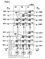
- FIG. 3 shows the first shift stage in a block diagram VS1, four each the small or large storage capacity K1.4 capacity information indicating EB1..4 application area ki over four capacity lines SZ0..3 and four the presence of memory modules SM in the application areas Configuration information displaying EB1..4 koi via four existing introductions VL0..3 to a multiplexer MUX can be managed.
- the MUX multiplexer has three sliding stages S1..3 on, the third shift stage S3 twice two (1..4), the second shift stage S2 three (5..10) and first shift stage S1 each four (11..18) multiplex elements MX contains.
- Half of the MX multiplex elements is the capacity lines SZ0..3 and the other half Existing instructions VL0..3 assigned.
- a multiplex element MX has two entrances - indicated by arrows - one Output and a control input - by the label ST indicated - on, whereby when creating a binary 0 information at the control input ST the ones at the upper input and when creating a binary 1 information to the Control input ST the signals present at the lower input can be switched to the output.
- the third shift stage S3 is the fourth introduction VL3 to one input of a first multiplex element MX (1), whose second input is connected to O potential and to an input of a second multiplex element MX (2) led, the second input with the third Presence initiation VL2 is connected.
- the third Shift stage S3 is also the fourth capacity line SZ3 to a third multiplex element MX (3), the second Input is connected to 0 potential, and to a fourth Multiplex element MX (4) switched, the second input with the third capacitance line SZ2 is connected.
- the exit of the second multiplex element MX (2) is at the upper input of the sixth and to the lower input of the seventh multiplex element MX (6,7) switched, the upper input with the second presence initiation VL1 is connected.
- the entrances of the eighth to tenth multiplex elements MX (8..10) are included the outputs of the third and fourth multiplex elements MX (3,4) connected in the same way as previously described.
- the output of the fifth is in the third shift stage S3 Multiplex element MX (5) with the upper entrance of the eleventh and the lower entrance of the twelfth multiplex element MX (11,12) connected, the lower input of the eleventh multiplex element MX (11) is switched to 0 potential.
- the output of the sixth multiplex element MX (6) is on the upper entrance of the twelfth and lower entrance of the thirteenth Multiplex element MX (12,13) and the output of the seventh multiplex element MX (7) is on the upper entrance of the thirteenth and the lower input of the fourteenth multiplex element MX (13,14) led, the upper entrance of the fourteenth multiplex element MX (14) with the first introduction VL0 is connected.
- the outputs of the eighth to tenth multiplex elements MX (8..10) and the first capacity line SZ0 with the upper ones and lower inputs of the fifteenth to eighteenth multiplex elements MX (15..18) connected.
- At the first introduction VL0 is an inverter IN1 switched, whose output to all control inputs ST the in the first shift stage S1 arranged multiplex elements MX (11..18) is performed.
- the control inputs are analogous to this ST of the second shift stage S2 via a second inverter IN2 with the second presence introduction VL1 and the control inputs ST of the third shift stage S3 via a third Inverter IN3 connected to the third presence initiation VL2.
- the outputs of the fourteenth to eleventh multiplex elements MX represent the logical introductions LVL0..3, on which the logical configuration information lkoi are available.
- the exits of the eighteenth to fifteenth multiplex elements MX (18..15) represent the logical capacity lines LSZ0..3, on which the logical Capacity information lki available.
- ki a binary 1 information a storage capacity of 4 Mbytes and 0 information represents a storage capacity of 1 Mbyte, lies in the embodiment on the first capacitance line SZ0 a 1 information on the second capacity line SZ1 a 0 information on the third capacity line SZ2 a 1 information and on the fourth capacity line SZ4 displays 0 information.
- a koi in the configuration information 0 information the absence and 1 information the presence indicates an inserted memory module SM based on the embodiment at the first introduction VL0 a binary 1 information, on the second Presence initiation VL1 a binary 0 information at which third presence initiation VL2 a binary 1 information and a binary 1 information at the fourth presence initiation VL3 on.
- FIG. 4 shows the capacity correction stage in a block diagram PPS.
- the four logical introductions LV0..3 are each with a further input of the first to fourth AND gate & (1..4) and one input from each fifth to eighth AND gates & (5-8) connected.
- the exit of the first AND gate & (1) is on a further input of the second and a further inverting input of the fifth AND gate & (2.5) performed.
- the exit of the second AND gate & (2) is on another input of the third and to another inverting input of the sixth AND gate & (3,6) switched.
- the output is analogous to this of the third AND gate & (3) with a further input of the fourth and with another inverting input of the seventh AND gate & (4,7) connected.
- the exit of the fourth AND gate & (4) is on another inverting input of the eighth AND gate & (8).
- the four exits K4 (0..3) of the four AND gates & (1..4) provide capacitance lines where the large storage capacity K4 logical capacity information klki are displayed. These capacitance lines are called K4 lines designated.
- the outputs of the fifth to eighth AND gates & (5..8) represent on the small storage capacity K1 related capacitance lines K1 (0..3), on which to the small Logical capacity information related to storage capacity klki are available.
- KKS will also be corrected to the effect that with regard to the assembly conditions - insertion of memory modules SM starting with the most significant address range EB1..4 - corrected incorrect assembly becomes.
- a memory module SM with a low storage capacity K1 is used, so be for the third and fourth application areas EB3,4 SM memory modules used only with low memory capacity K1 considered, although memory modules may be SM with large storage capacity K4 are used.
- FIG. 5 The components shown in Figure 5 and Figure 6 show together the module selection unit MAE - see Figure 2.
- Figure 5 are the two least significant address lines ADL2,3 the n + k most significant address lines ADL0-3 to a first one Decoding unit DK-1, and the two high-quality address lines ADL0.1 led to a second decoding unit DK-4.
- decoding units DK-1, DK-4 are the two Address lines ADL0.1, ADL2.3 to four, one each Application area EB1..4 assigned output lines A1..4 decoded.
- the output lines A1..4 of the second decoding unit DK-4 are each with an input of four AND gates & (1..4) connected.
- the second to fourth output lines A2..4 are also each with an input from fifth to seventh AND gates & (5..7) connected.
- the four output lines A1..4 of the first decoding unit DK-1 are connected to a first one Shift stage S1 performed and in this one Input of two multiplex elements MX switched.
- the other one free input of the fourth multiplex element MX is at zero potential 0 coupled.
- the output of the least significant multiplex element MX is with an input of an eighth AND gate & (8) and the outputs of the three other multiplex elements MX are each with an input of multiplex elements MX connected to a second shift stage S2.
- the exit of the least significant multiplex element MX is with a ninth AND gate & (9) and the outputs of the remaining two Multiplex elements MX each with an input of two further multiplex elements forming a third shift stage S3 MX led.
- the exit of the lower order Multiplex element MX is with the input of a tenth AND gate & (10) and the output of the remaining multiplex element MX with an input of an eleventh AND gate & (11) connected.
- the further input of the fourth AND gate & (4) is with the fourth K4 line K4 (3) and another input of the third AND gate & (3) is on the further input of the seventh AND gate & (7), the third K4 line K4 (2) and on the Control input ST of the third shift stage S3 switched. Analogous this is another input of the second AND gate & (2) to another input of the sixth AND gate & (6), on the second K4 line K4 (1) and on the control input ST of the second shift stage S2 performed.
- Another Input of the first AND gate & (1) assigns a connection a further input of the fifth AND gate & (5), the first K4 line K4 (0) and a control input ST of the first Shift level S1 up.
- the outputs are the fifth to the seventh AND gate & (5..7) in a first OR gate OD1 combined, its output with an enable input EN of the first decoding unit DK-1 is connected.
- the Outputs of the first to fourth AND gate & (1..4) are open a second OR gate OD2 coupled, its inverting Exit to another entrance of the eighth to eleventh AND gate & (8..11) are switched.
- Figure 6 shows four OR gates OD (1..4), at one entrance the respective output EN4 (0..3) of the first to fourth AND gate & (1..4) - see Figure 5 - and their others Input one output EN1 (0..3) each of the eighth to eleventh AND gate & (8..11) is performed.
- the outputs of the four OR gates OD1 (1..4) are each on an input of four AND gates & (1..4) switched.
- To the other entrances of the four AND gate & (1..4) is one of the four logical introductions LVL0..3 managed.
- the four AND gate & (1..4) is now the logic memory drive signal lsas before. This logic memory drive signal lsas shows in binary form which application area EB1..4 should be controlled logically.
- the conversion of the logic memory drive signal lsas in the physical memory drive signal sas is in FIG. 7 shown. To do this, the four introductions VL0..3 - see Figure 3 - to a third decoding unit DK-3 guided. The four outputs A1..A4 of the third decoding unit DK-3 are each with a control input ST of four sliding levels S1..4 connected.
- the sliding stages S1..4 are in the same way as in FIG. 3 or 5, realized.
- the third decoding unit DK-3 contains a decoding table, not shown, through which the sliding stages S1..4 are controlled in this way be that at the four outputs EN0..3 of the four sliding stages S1..4 the memory control signal sas is in binary form, one output each EN0..3 separately with one Application area EB1..4 is connected. This means that a the four outputs EN0..3 have binary 1 information, through which the used in the relevant application area EB1..4 Memory module SM controlled, that is, released becomes.
- the sub memory area in the released memory module SM controlled and by the microprocessor MP transmitted data saved or data read and transmitted to the microprocessor MP. Based on the The embodiment in the third area of application EB3 used memory module SM released, that is, addressed.
Description
- FIG 1
- eine Konfiguration eines Speichers mit der erfindungsgemäßen Konvertierungseinrichtung,
- FIG 2
- ein Blockschaltbild der Konvertierungseinrichtung,
- FIG 3
- die erste Verschiebestufe zur Bildung der logischen Kapazitäts- und Konfigurationsinformationen,
- FIG 4
- eine Kapazitätskorrekturstufe zum Bilden von Korrekturinformationen,
- FIG 5
- in einem Blockschaltbild eine Modulauswahleinheit
- FIG 6
- zum Bilden von logischen Speicheransteuersignalen und
- FIG 7
- eine zweite Verschiebestufe zur Bildung von physikalischen Speicheransteuersignalen.
- Ausgang LEN0 auf einen Eingang der vierten Schiebestufe S4,
- Ausgang LEN1 auf einen Eingang der vierten und dritten Schiebestufe S3, S4,
- der Ausgang LEN2 auf einen Eingang der zweiten, dritten und vierten Schiebestufe S2..4 und
- LEN3 auf jeweils einen Eingang aller vier Schiebestufen S1..4.
Claims (12)
- Verfahren zum Konvertieren von durch eine prozessorgesteuerte Einrichtung gebildeten Speicherbereichsadressen (AD0..m) in auf eine Struktur und Speicherkapazität eines Speichers (SP) abgestimmte Speicheransteuersignale (sas) anhand von Konvertierungsinformationen,bei dem der Speicher (SP) durch einheitliche und/oder unterschiedliche Speicherkapazitäten (K1,4) aufweisende Speichermodule (SM) gebildet ist, die jeweils in einen physikalischen Einsetzbereich (EB1..4) des Speichers (SP) eingesetzt sind, wobei der Speicher (SP) zumindest zwei Einsetzbereiche (EB1..4) umfaßt,bei dem jeweils jedem eingesetzten Speichermodul (SM) zugeordnete und die Speicherkapazität (K1,4) der jeweiligen eingesetzten Speichermodule (SM) anzeigende Kapazitätsinformationen (ki) und das Vorhandensein von eingesetzten Speichermodulen (SM) anzeigende Konfigurationsinformationen (koi) aller Einsetzbereiche (EB1..4) erfaßt werden, undbei dem aus den erfaßten Kapazitätsinformationen (ki) und den Konfigurationsinformationen (koi) in Abhängigkeit von den erfaßten Konfigurationsinformationen (koi) den Adreßraum anzeigende logische Kapazitätsinformationen (lki) und die virtuelle Konfiguration des Speichers (SP) anzeigende, logische Konfigurationsinformationen (lkoi) abgeleitet werden,wobei die logischen Kapazitäts- zusammen mit den Konfigurationsinformationen (lki,lkoi) die Konvertierungsinformationen repräsentieren, anhand derer die Speicheransteuersignale (sas) abgeleitet werden.
- Verfahren nach Anspruch 1, dadurch gekennzeichnet,daß bei einer m-stelligen, binären Speicherbereichsadresse (AD0..m) n höchstwertige Stellen für die Konfiguration von 2n Einsetzbereichen (EB1..4) vorgesehen werden,wobei in jeden der 2n Einsetzbereiche (EB1..4) Speichermodule (SM) mit einer Gesamtspeicherkapazität von 2m-n adressierbaren Speicherbereichen einsetzbar sind, unddaß für jeden Einsetzbereich (EB1..4) eine Kapazitäts- und eine Konfigurationsinformation (ki,koi) erfaßt wird.
- Verfahren nach Anspruch 2, dadurch gekennzeichnet,daß Speichermodule (SM) mit zwei unterschiedlichen Speicherkapazitäten (K1,4) einsetzbar sind, wobei die größere Speicherkapazität (K4) 2m-n adressierbare Speicherbereiche und die kleinere Speicherkapazität (K1) 2m-n-k (k,m,n = 1,2..) adressierbare Speicherbereichen umfaßt,daß die Speichermodule (SM) mit der größeren Speicherkapazität (K4), beginnend mit dem Einsetzbereich (EB1..4) mit den kleinsten, zugeordneten Speicherbereichsadressen (AD0..3), sukzessive in die Einsetzbereiche (EB1..4) mit den nächst höherwertigeren, zugeordneten Speicherbereichsadressen (AD0..3) eingesetzt werden,daß die erfaßte Kapazitätsinformationen (ki) durch eine die kleine oder große Speicherkapazität (K1,4) anzeigende, binäre Kapazitätsinformationund die Konfigurationsinformation (koi) durch eine das Vorhandensein oder Nichtvorhandensein eines eingesetzten Speichermoduls (SM) anzeigende, binäre Konfigurationsinformation repräsentiert ist.
- Verfahren nach Anspruch 3, dadurch gekennzeichnet,daß nach dem Einsetzen von Speichermodulen (SM) in die Einsetzbereiche (EB1..4) die logischen Kapazitätsinformationen (lki) derart gebildet werden,daß ausgehend von den ein eingesetztes Speichermodul (SM) aufweisenden Einsetzbereichen (EB1..4) mit den zugeordneten niedrigsten Speicherbereichsadressen (AD0..3) beim Vorliegen einer ein eingesetztes Speichermodul (SM) anzeigenden Konfigurationsinformation (koi) die jeweils erfaßten, binären Kapazitätsinformationen (ki) binär addiert werden und eine Dualzahl darstellen, die den nutzbaren Adreßraum des Speichers (SP) durch die duale Summe der großen Speicherkapazitäten (K4) angibt.
- Verfahren nach Anspruch 4, dadurch gekennzeichnet,daß bei Einsetzbereichen (EB1..4) ohne eingesetzte Speichermodule (SM) die logische Kapazitätsinformation (lki) und die logische Konfigurationsinformation (lkoi) in Abhängigkeit vom Vorhandensein von eingesetzten Speichermodulen (SM) durch Verschieben der die Speicherkapazität (K1,4) von Speichermodulen (SM) anzeigenden, binären Kapazitäts- und Konfigurationsinformationen (ki,koi) in Richtung niederwertige Stellen der mehrstelligen, binären Kapazitäts- und Konfigurationsinformationen (ki,koi) erfolgt.
- Anordnung zum Konvertieren von durch eine prozessorgesteuerte Einrichtung gebildeten Speicherbereichsadressen (AD0..m) in auf eine Struktur und Speicherkapazität eines Speichers (SP) abgestimmte Speicheransteuersignale (sas) anhand von Konvertierungsinformationen,bei der der Speicher (SP) durch einheitliche und/oder unterschiedliche Speicherkapazitäten (K1,4) aufweisende Speichermodule (SM) gebildet ist, die jeweils in einen physikalischen Einsetzbereich (EB1..4) des Speichers (SP) eingesetzt sind, wobei der Speicher (SP) zumindest zwei Einsetzbereiche (EB1..4) umfaßt,bei der Kapazitäts- und Vorhandenseinleitungen (SZ,VL), über die jeweils jedem eingesetzten Speichermodul (SM) zugeordnete und die Speicherkapazität (K1,4) der jeweiligen eingesetzten Speichermodule (SM) anzeigende Kapazitätsinformationen (ki) und das Vorhandensein von eingesetzten Speichermodulen (SM) anzeigende Konfigurationsinformationen (koi) aller Einsetzbereiche (EB1..4) übermittelt werden, an eine Verschiebestufe (VS1) angeschlossen sind, undbei der die Verschiebestufe (VS1) derart ausgestaltet ist, daß aus den erfaßten Kapazitätsinformationen (ki) und den Konfigurationsinformationen (koi) in Abhängigkeit von den erfaßten Konfigurationsinformationen (koi) den Adreßraum anzeigende logische Kapazitätsinformationen (lki) und die virtuelle Konfiguration des Speichers (SP) anzeigende, logische Konfigurationsinformationen (lkoi) abgeleitet werden,wobei die die logischen Kapazitäts- zusammen mit den Konfigurationsinformationen (lki,lkoi) repräsentierenden Konvertierungsinformationen an jeweils einem Ausgang (A1,2) der Verschiebestufe (VS1) vorliegen, und wobeieine Konvertierungseinrichtung (KVE) zum Ableiten der Speicheransteuersignale (sas) anhand der Konvertierungsinformationen vorgesehen ist.
- Verfahren nach Anspruch 1,
dadurch gekennzeichnet,daß aus n, die Konfiguration des Speichers betreffenden Stellen einer aktuell vorliegenden m-stelligen Speicherbereichsadresse (AD0..m) mit Hilfe der logischen Kapazitätsinformationen (lkio) und der logischen Konfigurationsinformationen (lkoi) einsetzbereichsbezogen ein logisches Speicheransteuersignal (lsas) abgeleitet wird, unddaß mit Hilfe der Konfigurationsinformationen (koi) aus dem einsetzbereichsbezogenen logischen Speicheransteuersignal (lsas) für den betroffenen Einsetzbereich ein physikalisches Speicheransteuersignal (sas) abgeleitet wird. - Verfahren nach Anspruch 7, dadurch gekennzeichnet,daß in jeden von 2n Einsetzbereichen 1..4) Speichermodule (SM) mit einer Gesamtspeicherkapazität von 2m-n adressierbaren Speicherbereichen einsetzbar sind,daß aus der n-stelligen Speicherbereichsadresse (AD0..3), mit Hilfe von aus den logischen Kapazitäts- und Konfigurationsinformationen (lki,lkoi) abgeleiteten speicherkapazitatsindividuellen Kapazitätsinformationen (klki) für jede vorgesehene Speicherkapazität (K1,4) logische Speicheransteuersignale (lsas1,lsas4) abgeleitet werden sowie anschließend mit Hilfe der logischen Konfigurationsinformationen (lkoi) ein logisches Speicheransteuersignal (lsas) gebildet wird, unddaß aus dem logischen Speicheransteuersignal (lsas) mit Hilfe der Konfigurationsinformationen ((koi)) für den ermittelten Einsetzbereich (EB1..4) ein physikalisches Speicheransteuersignal (sas) gebildet und an das Speichermodul (SM) des betroffenen Einsetzbereichs (EB1..4) weitergeleitet wird.
- Verfahren nach Anspruch 8, dadurch gekennzeichnet, daß aus den logischen Kapazitäts- und Konfigurationsinformationen (lki,lkoi) für jede mögliche Speicherkapazität (K1,4) jeweils deren logische Gesamtspeicherkapazität anzeigende, logische speicherkapazitätsindividuelle Kapazitätsinformationen (klki) gebildet werden.
- Verfahren nach Anspruch 8 oder 9, dadurch gekennzeichnet, daß aus den aktuell vorliegenden Adreßinformationen der m-stelligen Speicherbereichsadresse (AD0..m) für jede vorgesehene Speicherkapazität (K1,4) abgeleitete logische Speicheransteuersignale (lsas1,4) auf die logischen Konfigurationsinformationen (lkoi) abgebildet werden, wodurch ein logisches Speicheransteuersignal (lsas) gebildet wird.
- Verfahren nach einem der Ansprüche 8 bis 10, dadurch gekennzeichnet, daß die Konfigurationsinformationen (koi) dekodiert das logische Speicheransteuersignal (lsas) auf den betroffenen Einsetzbereich (EB1..4) steuern, wobei das gesteuerte logische Speicheransteuersignal (lsas) das physikalische Speicheransteuersignal (sas) repräsentiert.
- Anordnung nach Anspruch 6,
dadurch gekennzeichnet,daß die die virtuelle Speicherkapazität anzeigenden, logischen Kapazitätsinformationen (lki) und die logischen Konfigurationsinformationen (lkoi) übermittelnde Kapazitätsund Konfigurationsleitungen (LSZ,LVL) an die Konvertierungseinrichtung (KVE) angeschlossen sind,daß die Konvertierungseinrichtung (KVE) derart ausgestaltet ist, daß aus n, die Konfiguration des Speichers betreffenden Stellen einer aktuell vorliegenden m-stelligen Speicherbereichsadresse (AD0..m) mit Hilfe der logischen Kapazitätsinformationen (lki) und der logischen Konfigurationsinformationen (lkoi) ein einsetzbereichsbezogenes logisches Speicheransteuersignal (lsas) abgeleitet wird,daß mit Hilfe der Konfigurationsinformationen (koi) aus dem einsetzbereichsbezogenen logischen Speicheransteuersignal (lsas) für den betroffenen Einsetzbereich (EB1..4) ein physikalisches Speicheransteuersignal (sas) abgeleitet wird, unddaß an jeden Einsetzbereich (EB1..4) ein das Speicheransteuersignal (sas) übermittelnder Ausgang (EN0..3 der Konvertierungseinrichtung (KVE) geschaltet ist.
Applications Claiming Priority (2)
| Application Number | Priority Date | Filing Date | Title |
|---|---|---|---|
| DE19549061 | 1995-12-29 | ||
| DE19549061 | 1995-12-29 |
Publications (2)
| Publication Number | Publication Date |
|---|---|
| EP0782077A1 EP0782077A1 (de) | 1997-07-02 |
| EP0782077B1 true EP0782077B1 (de) | 2003-08-20 |
Family
ID=7781601
Family Applications (1)
| Application Number | Title | Priority Date | Filing Date |
|---|---|---|---|
| EP96119487A Expired - Lifetime EP0782077B1 (de) | 1995-12-29 | 1996-12-04 | Verfahren und Anordnung zum Konvertieren von Speicheradressen in Speicheransteuersignale |
Country Status (5)
| Country | Link |
|---|---|
| US (1) | US6003110A (de) |
| EP (1) | EP0782077B1 (de) |
| JP (1) | JP3266529B2 (de) |
| DE (1) | DE59610672D1 (de) |
| SG (1) | SG46760A1 (de) |
Families Citing this family (6)
| Publication number | Priority date | Publication date | Assignee | Title |
|---|---|---|---|---|
| JPH09293015A (ja) * | 1996-04-24 | 1997-11-11 | Mitsubishi Electric Corp | メモリシステムおよびそれに用いられる半導体記憶装置 |
| JP3365283B2 (ja) * | 1997-11-14 | 2003-01-08 | 日本電気株式会社 | 半導体記憶装置 |
| JP3498021B2 (ja) | 1999-10-07 | 2004-02-16 | エヌイーシーコンピュータテクノ株式会社 | メモリ制御方式 |
| GB2357602A (en) | 1999-12-22 | 2001-06-27 | Nokia Mobile Phones Ltd | Memory controller for a memory array comprising different memory types |
| US7339837B2 (en) * | 2004-05-18 | 2008-03-04 | Infineon Technologies Ag | Configurable embedded processor |
| US7308527B2 (en) * | 2005-01-24 | 2007-12-11 | International Business Machines Corporation | System for indicating a plug position for a memory module in a memory system |
Family Cites Families (7)
| Publication number | Priority date | Publication date | Assignee | Title |
|---|---|---|---|---|
| US4908789A (en) * | 1987-04-01 | 1990-03-13 | International Business Machines Corporation | Method and system for automatically assigning memory modules of different predetermined capacities to contiguous segments of a linear address range |
| US4888687A (en) * | 1987-05-04 | 1989-12-19 | Prime Computer, Inc. | Memory control system |
| US5119486A (en) * | 1989-01-17 | 1992-06-02 | Prime Computer | Memory board selection method and apparatus |
| JPH0715665B2 (ja) * | 1991-06-10 | 1995-02-22 | インターナショナル・ビジネス・マシーンズ・コーポレイション | パーソナルコンピユータ |
| DE59206051D1 (de) * | 1992-02-28 | 1996-05-23 | Siemens Ag | Verfahren zur hierarchisch administrierbaren kennungsorientierten Freigabesteuerung für bedieneraufgabenbezogene Zugriffsanweisungen auf eine Datenbasis einer programmgesteuerten Kommunikationsanlage |
| US5446860A (en) * | 1993-01-11 | 1995-08-29 | Hewlett-Packard Company | Apparatus for determining a computer memory configuration of memory modules using presence detect bits shifted serially into a configuration register |
| EP0629952B1 (de) * | 1993-06-16 | 1999-09-01 | Bull HN Information Systems Italia S.p.A. | Speicher mit variabeler Verschachtelungshöhe und verwandte Konfigurationseinheit |
-
1996
- 1996-12-04 EP EP96119487A patent/EP0782077B1/de not_active Expired - Lifetime
- 1996-12-04 DE DE59610672T patent/DE59610672D1/de not_active Expired - Lifetime
- 1996-12-10 SG SG1996011616A patent/SG46760A1/en unknown
- 1996-12-25 JP JP34590196A patent/JP3266529B2/ja not_active Expired - Fee Related
- 1996-12-30 US US08/774,459 patent/US6003110A/en not_active Expired - Lifetime
Also Published As
| Publication number | Publication date |
|---|---|
| EP0782077A1 (de) | 1997-07-02 |
| JP3266529B2 (ja) | 2002-03-18 |
| SG46760A1 (en) | 1998-02-20 |
| US6003110A (en) | 1999-12-14 |
| DE59610672D1 (de) | 2003-09-25 |
| JPH09212413A (ja) | 1997-08-15 |
Similar Documents
| Publication | Publication Date | Title |
|---|---|---|
| DE2030760C2 (de) | Paritätsprüfschaltung für eine Speicherschaltung | |
| WO2002039280A2 (de) | Softwarewerkzeug zur überwachung eines automatisierungsgerätes auf störungen | |
| DE3015875A1 (de) | Speicherzugriffssystem und verfahren fuer einen zugriff zu einem digitalen speichersystem | |
| DE2926322C2 (de) | Speicher-Subsystem | |
| DE3043100C2 (de) | ||
| DE3618136C2 (de) | ||
| DE2261786B2 (de) | Festwert-Speichereinheit | |
| DE2213953C3 (de) | Schaltungsanordnung zum Darstellen von Zeichen auf dem Bildschirm eines Sichtgerätes | |
| DE4431304C2 (de) | Steuerschaltung für die Farbsteuerung einer Anzeigevorrichtung in unterschiedlichen Betriebsarten | |
| EP0782077B1 (de) | Verfahren und Anordnung zum Konvertieren von Speicheradressen in Speicheransteuersignale | |
| DE2420214A1 (de) | Ein/ausgabe-vermittlung mit ausfallausgleich | |
| DE3024153A1 (de) | Speicher-subsystem | |
| DE4239461A1 (de) | Anordnung zur Übertragung von Daten über einen Bus | |
| DE3324313A1 (de) | Einrichtung zur signaltechnisch sicheren darstellung von information auf einem datensichtgeraet | |
| DE1234054B (de) | Byte-Umsetzer | |
| DE10105627B4 (de) | Mehrfachanschlussspeichereinrichtung, Verfahren und System zum Betrieb einer Mehrfachanschlussspeichereinrichtung | |
| DE2235883A1 (de) | Datenverarbeitungseinrichtung | |
| DE2419733B2 (de) | Schaltungsanordnung zur wiedergabe von als mehrstellige binaer-zahlen codierten daten als alphanumerische zeichen in form einer 7x5-matrix | |
| DE2233164A1 (de) | Schaltungsanordnung zur ausblendung eines beliebig waehlbaren bereichs einer bitfolge bei deren uebertragung zwischen zwei registern | |
| DE2017879B2 (de) | Speicheranordnung mit freiem Zugriff | |
| DE10208073A1 (de) | Treiberschaltung für eine LCD-Anzeige | |
| EP0480331A2 (de) | Datenverarbeitungssystem mit Bildschirmeinheiten | |
| DE2551981C3 (de) | Prüfanordnung für eine Datenausgabeeinrichtung | |
| DE4107007A1 (de) | Elektronisches geraet | |
| DE4439840C1 (de) | Simulationssystem zur Simulation von Displays |
Legal Events
| Date | Code | Title | Description |
|---|---|---|---|
| PUAI | Public reference made under article 153(3) epc to a published international application that has entered the european phase |
Free format text: ORIGINAL CODE: 0009012 |
|
| AK | Designated contracting states |
Kind code of ref document: A1 Designated state(s): DE FR GB IT NL |
|
| 17P | Request for examination filed |
Effective date: 19970721 |
|
| 17Q | First examination report despatched |
Effective date: 20010730 |
|
| GRAH | Despatch of communication of intention to grant a patent |
Free format text: ORIGINAL CODE: EPIDOS IGRA |
|
| GRAS | Grant fee paid |
Free format text: ORIGINAL CODE: EPIDOSNIGR3 |
|
| GRAA | (expected) grant |
Free format text: ORIGINAL CODE: 0009210 |
|
| AK | Designated contracting states |
Designated state(s): DE FR GB IT NL |
|
| PG25 | Lapsed in a contracting state [announced via postgrant information from national office to epo] |
Ref country code: NL Free format text: LAPSE BECAUSE OF FAILURE TO SUBMIT A TRANSLATION OF THE DESCRIPTION OR TO PAY THE FEE WITHIN THE PRESCRIBED TIME-LIMIT Effective date: 20030820 |
|
| REG | Reference to a national code |
Ref country code: GB Ref legal event code: FG4D Free format text: NOT ENGLISH |
|
| REF | Corresponds to: |
Ref document number: 59610672 Country of ref document: DE Date of ref document: 20030925 Kind code of ref document: P |
|
| GBT | Gb: translation of ep patent filed (gb section 77(6)(a)/1977) | ||
| NLV1 | Nl: lapsed or annulled due to failure to fulfill the requirements of art. 29p and 29m of the patents act | ||
| ET | Fr: translation filed | ||
| PLBE | No opposition filed within time limit |
Free format text: ORIGINAL CODE: 0009261 |
|
| STAA | Information on the status of an ep patent application or granted ep patent |
Free format text: STATUS: NO OPPOSITION FILED WITHIN TIME LIMIT |
|
| REG | Reference to a national code |
Ref country code: HK Ref legal event code: WD Ref document number: 1000843 Country of ref document: HK |
|
| 26N | No opposition filed |
Effective date: 20040524 |
|
| REG | Reference to a national code |
Ref country code: GB Ref legal event code: 732E Free format text: REGISTERED BETWEEN 20121025 AND 20121031 |
|
| REG | Reference to a national code |
Ref country code: FR Ref legal event code: TP Owner name: SIEMENS ENTERPRISE COMMUNICATIONS GMBH & CO. K, DE Effective date: 20130108 |
|
| REG | Reference to a national code |
Ref country code: DE Ref legal event code: R082 Ref document number: 59610672 Country of ref document: DE Representative=s name: FRITZSCHE PATENT, DE |
|
| REG | Reference to a national code |
Ref country code: DE Ref legal event code: R082 Ref document number: 59610672 Country of ref document: DE Representative=s name: FRITZSCHE PATENTANWAELTE, DE Effective date: 20130313 Ref country code: DE Ref legal event code: R082 Ref document number: 59610672 Country of ref document: DE Representative=s name: FRITZSCHE PATENT, DE Effective date: 20130313 Ref country code: DE Ref legal event code: R081 Ref document number: 59610672 Country of ref document: DE Owner name: UNIFY GMBH & CO. KG, DE Free format text: FORMER OWNER: SIEMENS AKTIENGESELLSCHAFT, 80333 MUENCHEN, DE Effective date: 20130313 Ref country code: DE Ref legal event code: R081 Ref document number: 59610672 Country of ref document: DE Owner name: SIEMENS ENTERPRISE COMMUNICATIONS GMBH & CO. K, DE Free format text: FORMER OWNER: SIEMENS AKTIENGESELLSCHAFT, 80333 MUENCHEN, DE Effective date: 20130313 |
|
| REG | Reference to a national code |
Ref country code: DE Ref legal event code: R082 Ref document number: 59610672 Country of ref document: DE Representative=s name: FRITZSCHE PATENT, DE |
|
| REG | Reference to a national code |
Ref country code: DE Ref legal event code: R082 Ref document number: 59610672 Country of ref document: DE Representative=s name: FRITZSCHE PATENTANWAELTE, DE Effective date: 20131112 Ref country code: DE Ref legal event code: R082 Ref document number: 59610672 Country of ref document: DE Representative=s name: FRITZSCHE PATENT, DE Effective date: 20131112 Ref country code: DE Ref legal event code: R081 Ref document number: 59610672 Country of ref document: DE Owner name: UNIFY GMBH & CO. KG, DE Free format text: FORMER OWNER: SIEMENS ENTERPRISE COMMUNICATIONS GMBH & CO. KG, 81379 MUENCHEN, DE Effective date: 20131112 |
|
| REG | Reference to a national code |
Ref country code: FR Ref legal event code: CD Owner name: UNIFY GMBH & CO.KG, DE Effective date: 20140429 |
|
| PGFP | Annual fee paid to national office [announced via postgrant information from national office to epo] |
Ref country code: GB Payment date: 20141216 Year of fee payment: 19 |
|
| PGFP | Annual fee paid to national office [announced via postgrant information from national office to epo] |
Ref country code: FR Payment date: 20141212 Year of fee payment: 19 |
|
| PGFP | Annual fee paid to national office [announced via postgrant information from national office to epo] |
Ref country code: IT Payment date: 20141218 Year of fee payment: 19 |
|
| PGFP | Annual fee paid to national office [announced via postgrant information from national office to epo] |
Ref country code: DE Payment date: 20151217 Year of fee payment: 20 |
|
| GBPC | Gb: european patent ceased through non-payment of renewal fee |
Effective date: 20151204 |
|
| REG | Reference to a national code |
Ref country code: DE Ref legal event code: R082 Ref document number: 59610672 Country of ref document: DE Representative=s name: FRITZSCHE PATENTANWAELTE, DE Ref country code: DE Ref legal event code: R081 Ref document number: 59610672 Country of ref document: DE Owner name: UNIFY GMBH & CO. KG, DE Free format text: FORMER OWNER: UNIFY GMBH & CO. KG, 81379 MUENCHEN, DE |
|
| REG | Reference to a national code |
Ref country code: FR Ref legal event code: ST Effective date: 20160831 |
|
| PG25 | Lapsed in a contracting state [announced via postgrant information from national office to epo] |
Ref country code: GB Free format text: LAPSE BECAUSE OF NON-PAYMENT OF DUE FEES Effective date: 20151204 |
|
| PG25 | Lapsed in a contracting state [announced via postgrant information from national office to epo] |
Ref country code: FR Free format text: LAPSE BECAUSE OF NON-PAYMENT OF DUE FEES Effective date: 20151231 |
|
| REG | Reference to a national code |
Ref country code: DE Ref legal event code: R071 Ref document number: 59610672 Country of ref document: DE |
|
| PG25 | Lapsed in a contracting state [announced via postgrant information from national office to epo] |
Ref country code: IT Free format text: LAPSE BECAUSE OF NON-PAYMENT OF DUE FEES Effective date: 20151204 |