EP0781993B1 - Gassensor - Google Patents
Gassensor Download PDFInfo
- Publication number
- EP0781993B1 EP0781993B1 EP96120427A EP96120427A EP0781993B1 EP 0781993 B1 EP0781993 B1 EP 0781993B1 EP 96120427 A EP96120427 A EP 96120427A EP 96120427 A EP96120427 A EP 96120427A EP 0781993 B1 EP0781993 B1 EP 0781993B1
- Authority
- EP
- European Patent Office
- Prior art keywords
- gas
- layer
- sensor according
- gas sensor
- electrically conducting
- Prior art date
- Legal status (The legal status is an assumption and is not a legal conclusion. Google has not performed a legal analysis and makes no representation as to the accuracy of the status listed.)
- Expired - Lifetime
Links
Images


Classifications
-
- G—PHYSICS
- G01—MEASURING; TESTING
- G01N—INVESTIGATING OR ANALYSING MATERIALS BY DETERMINING THEIR CHEMICAL OR PHYSICAL PROPERTIES
- G01N27/00—Investigating or analysing materials by the use of electric, electrochemical, or magnetic means
- G01N27/02—Investigating or analysing materials by the use of electric, electrochemical, or magnetic means by investigating impedance
- G01N27/04—Investigating or analysing materials by the use of electric, electrochemical, or magnetic means by investigating impedance by investigating resistance
- G01N27/12—Investigating or analysing materials by the use of electric, electrochemical, or magnetic means by investigating impedance by investigating resistance of a solid body in dependence upon absorption of a fluid; of a solid body in dependence upon reaction with a fluid, for detecting components in the fluid
Definitions
- Resistive gas sensors are based on the property of special ones gas sensitive materials. Their electrical properties change in the presence of certain gases depending on their concentration in a more characteristic and reproducible way Wise. The detection of the change in conductivity of the gas-sensitive Materials are mostly electrical. To do this, the gas-sensitive material is e.g. connected to an electrical voltage source in such a way that there is an electrical circuit.
- resistive gas sensors in the exhaust tract of an internal combustion engine used to detect the presence of certain gases
- the resistive gas sensor must be detected before mechanical ones and to protect against chemical influences.
- This can be done through a at least partially gas-permeable protective layer (sacrificial layer), which is applied to the gas sensitive element can be achieved, see DE 43 39 737 C1.
- the Protective layer in turn have electrical conductivity and can also be gas sensitive an undesirable and difficult to control electrical parallel resistance to the actual sensor resistance.
- the protective layer can be influenced the attacking media and their chemical composition as well as their electrical conductivity change what additional in a drift-like change in the sensor characteristic noticeable.
- the resistance of the Protective layer strongly dependent on temperature. So that's the influence the protective layer on the measurement accuracy also strongly temperature-dependent.
- GB-A-2142147 describes a gas sensor which has a planar structure of the measuring electrodes, which are partially covered by a gas-sensitive layer, which in turn is partially covered by a very thin metal layer.
- the metal layer is not electrically contacted and only imperfectly covers the electrodes.
- the thickness of the metal layer is typically 20 ⁇ and serves to modify the electrical properties of the gas-sensitive layer and / or to catalyze the reaction of gases with the semiconducting surface.
- GB-A-2029583 describes a resistive gas sensor in which a plurality of electrodes are applied on one side of a gas-sensitive resistance layer and a palladium film on the other side of the resistance layer. The very fine-grained palladium film is used for catalysis.
- the sensor temperature must therefore be kept exactly constant become what under the typical environmental conditions, for example, in the case of rapid gas flows in the exhaust tract, extraordinary is difficult and in any case a quick one and requires precise temperature control.
- the object of the invention is to provide a gas sensor where the sensor drift is minimized.
- the object is achieved by a gas sensor according to claim 1 solved.
- the gas sensor according to claim 2 has the advantage of an increased mechanical stability.
- an insulation layer between the measuring electrode structure and the substrate can according to claim 3, an insulation layer between the measuring electrode structure and the substrate.
- a protective layer can be provided according to claim 4 his.
- the gas sensor according to claim 6 has the advantage that the characteristic of the gas sensor, that is the sensitivity and the cross sensitivity to certain types of gas, through a appropriate choice of the catalyst specifically changed and can be adjusted. It can also by the catalyst the slope of the sensor characteristic can be influenced.
- the gas sensor according to claim 7 has the advantage of a large one Universality, because instead of a purely metallic one electrically conductive layer, for example metal oxides and ceramics or even organic substances such as phthalocyanine can be used. Metal oxides and ceramics for example, are characterized by a very high temperature resistance out. By using organic materials can, on the other hand, catalyze specific chemical reactions be, the reaction products in turn by the gas sensitive Layer can be detected.
- the top electrode can also have a filter effect, so that only certain types of gas penetrate the cover electrode and can be detected by the gas sensitive layer. Hereby can, for example, improve the selectivity of the sensor become.
- the gas sensor can be operated according to Claim 8 be formed.
- the gas access to gas sensitive Shift is increased.
- the gas sensor can be designed according to claim 11 his.
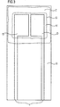
- the sensor according to the invention shown in cross section in FIG. 1 has a substrate S, over which an electrical Insulation layer I is provided.
- the presence of the electrical insulation layer I is optional and only with one Substrate S with interfering intrinsic conductivity necessary.
- the gas sensitive layer G is partial (compare Figure 1) or entirely with a shielding electrode V, also referred to below as an electrically conductive layer, Mistake. Again, a protective layer Z is applied.
- the presence of the protective layer Z is not absolutely necessary. Whether the protective layer Z must be present and in the thickness to be carried out depends on the respective application of the sensor.
- the senor is equipped with a heating arrangement to provide. This is not shown in Figure 1.
- the shielding electrode V (in the following also as a shielding layer serves as the equipotential surface for the electric field E over the measuring electrodes D, which here too referred to as base electrodes become.
- the shield electrode V has none electrical connections.
- FIG. 2 shows a perspective view of the measuring electrodes D and the shielding electrode V of the sensor, with L being the supply lines of the measuring electrodes D. These are connected to a supply voltage source which generates a voltage U 0 and to a current measuring device SMG. After the voltage U 0 is applied, an electric field E is formed between the measuring electrodes D and the shielding electrode V.
- the arrangement of the base electrodes D and the shielding electrode V corresponds essentially to that of two series connected Plate capacitors with a plate spacing d and a gas sensitive, electrically conductive dielectric, which in this case represents the gas sensitive layer G.
- the electric field E is therefore in the range between limits the measuring electrodes D and the shielding electrode V, whereby the vector of the electric field strength E (with the exception the marginal areas to be neglected) orthogonal to the Electrode surfaces.
- the by the voltage source in current produced by the electrical circuit, which is a measure of is the gas concentration, as well as its changes displayed by the ammeter SMG.
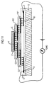
- the top view of the sensor is shown in FIG.
- the areal base electrodes D are on the surface of the substrate S, which may with a Insulation layer I (not shown in Figure 3) is.
- the conductor tracks L, with which are used for power supply the measuring electrodes D are connected.
- the gas sensitive Layer G Between the measuring electrodes D and the gas-permeable shielding electrode V, which over the measuring electrodes D is located, the gas sensitive Layer G.
- the active sensor area is marked with a gas-permeable protective layer Z covered.
- the sensor heater is conveniently located on the back of the Substrate S arranged in the region of the active sensor material G. and dimensioned so that one in this area as possible homogeneous temperature distribution is achieved.
- the conductor tracks L with a additional cover layer may be provided (in the figures Not shown).
- a particularly low-resistance sensor resistor can also be used here through so-called interdigital structures, i.e. comb-like structures nested structures for the measuring electrodes D can be achieved.
- the interdigital electrodes can both serve for power supply as well as for potential tapping.
- the finger spacing of the electrodes is typically 1 ⁇ m to 100 ⁇ m.
- metallic elements are used for the measuring electrodes D. or metallic compounds used.
- the shielding layer V can also be closed, which in the Figures is not shown. Diffusion through the shielding layer V is also a gas inlet in this case gas sensitive layer G possible.
- the individual are strip-shaped Conductor tracks of the shielding layer V with a certain Spaced from each other so that through the gaps between the individual conductor tracks of the shielding electrode good gas passage to the gas sensitive below Layer G is possible.
- the structure shown in FIG. 7 is additionally characterized by a good one Response behavior.
- FIG. 9 shows a top view of one according to that described in FIG. 8 Principle of a gas sensor with a base electrode D, which has four conductor tracks.
- the shield electrode V can also be different Species can be layered vertically. An embodiment this is shown in FIG. 10. By using it different materials for the electrodes D, W, and V and especially through the use of different gas sensitive Materials for layers G1 and G2 and through different layer thicknesses for these layers G1 and G2 can change the sensor properties in wide areas or be specifically adapted to the requirements.
- the base electrode D and various shield electrode structures V, W1, W2 can ultimately implement arrangements as shown in Figure 11. This allows the advantages of a long current path with good gas access and the possibilities of different materials for the individual horizontal positions of the shielding electrodes W1, W2 of the base electrode D and the top electrode V and for the individual gas-sensitive layers G1, G2 and G3 combined become.
- the overlap of the individual gas-sensitive layers G1, G2 and G3 is also chosen so that the respective upper layer as a protective layer for the gas sensitive below Layer serves. That is, layer Z serves to protect the active area of the gas sensitive layer G3.
- the gas sensitive Layer G3 serves to protect the active area of the gas sensitive layer G2 and the gas sensitive layer G2 serves to protect the active area of the gas sensitive Layer G1.
- the individual shielding electrodes V, W2 and W1 also here executed in the form of a strip in the manner already illustrated become.
Landscapes
- Chemical & Material Sciences (AREA)
- Analytical Chemistry (AREA)
- Electrochemistry (AREA)
- Physics & Mathematics (AREA)
- Health & Medical Sciences (AREA)
- Life Sciences & Earth Sciences (AREA)
- Chemical Kinetics & Catalysis (AREA)
- Biochemistry (AREA)
- General Health & Medical Sciences (AREA)
- General Physics & Mathematics (AREA)
- Immunology (AREA)
- Pathology (AREA)
- Investigating Or Analyzing Materials By The Use Of Fluid Adsorption Or Reactions (AREA)
- Investigating Or Analyzing Materials By The Use Of Electric Means (AREA)
Description
In GB-A-2029583 wird ein resistiver Gassensor beschrieben, bei dem mehrere Elektroden auf einer Seite einer gassensitiven Widerstandsschicht aufgebracht sind, und ein Palladiumfilm auf der anderen Seite der Widerstandsschicht. Der sehr feinkörnige Palladiumfilm dient der Katalyse.
- Figur 1
- den prinzipiellen Aufbau des erfindungsgemäßen Sensors,
- Figur 2
- eine perspektivische Ansicht der Elektroden des erfindungsgemäßen Sensors,
- Figur 3
- eine Draufsicht des erfindungsgemäßen Sensors,
- Figur 4
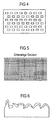
- eine erste mögliche Ausgestaltungsform der Abschirmschicht,
- Figur 5
- eine zweite mögliche Ausgestaltungsform der Abschirmschicht,
- Figur 6
- eine dritte Ausgestaltungsform der Abschirmschicht,
- Figur 7
- eine Draufsicht, wobei die Deckelektrode streifenförmig ausgebildet ist,
- Figur 8
- eine weitere Ausführungsform des Gassensors im Querschnitt, bei dem sowohl die Grundelektrode als auch die Deckelektrode mehrere Leiterbahnen aufweisen,
- Figur 9
- eine Draufsicht der in Figur 8 gezeigten Ausführungsform des Gassensors,
- Figur 10
- eine weitere Ausführungsform des Gassensors im Querschnitt, bei dem die gassensitive Schicht zweilagig aufgebracht ist und zwischen den beiden Lagen eine zweite Abschirmelektrode eingebracht ist, und
- Figur 11
- eine weitere Ausführungsform des Gassensors im Querschnitt, bei dem die gassensitive dreilagige Schicht treppenförmig angeordnet ist und zwischen den Lagen jeweils Abschirmelektroden eingebracht sind.
Claims (16)
- Gassensor bestehend aus:dadurch gekennzeichnet, daßeiner gassensitiven Schicht (G),einer Meßelektrodenstruktur (D) auf einer Sei der gassensitiven Schicht (G),einer der Meßelektrodenstruktur (D) auf der anderen Seit der gassensitiven Schicht (G) gegenüberliegende Schicht (V), die elektrisch nicht kontaktiert ist,
die gegenüberliegende Schicht (V)elektrisch leitend ist und ihre laterale Ausdehnung ungefähr der Meßelektrodenstruktur (G) entspricht,elektrisch abschirmend wirkt und einen Stromfluß durch die gassensitive Schicht (G) leitet. - Gassensor nach Anspruch 1,
bei dem ein Substrat (S) vorgesehen ist, das die Meßelektrodenstruktur (D), die gassensitive Schicht (G) und die elektrisch leitende Schicht (V) trägt. - Gassensor nach Anspruch 1 oder 2,
bei dem zwischen der Meßelektrodenstruktur (D) und dem Substrat (S) eine Isolationsschicht (I) vorgesehen ist. - Gassensor nach einem der Ansprüche 1 - 3,
bei dem die gassensitive Schicht (G) und die elektrisch leitende Schicht (V) mit einer Schutzschicht (Z) überzogen sind. - Gassensor nach einem der Ansprüche 1 - 4,
bei dem die gassensitive Schicht (G) Strontiumtitanat Bariumtitanat, Vanadiumoxid, Galliumoxid, Ceroxid, Bariumstanat oder Zinkoxid aufweist. - Gassensor nach einem der Ansprüche 1 - 5,
bei dem die elektrisch leitende Schicht (V) ein katalytisch aktives Material aufweist. - Gassensor nach einem der Ansprüche 1 - 5,
bei dem die elektrisch leitende Schicht (V) ein Metalloxid, eine Keramik oder ein organisches Material aufweist. - Gassensor nach einem der Ansprüche 1 - 7,
bei dem die elektrisch leitende Schicht (V) eine poröse oder löchrige Struktur aufweist. - Gassensor nach einem der Ansprüche 4 - 8,
bei dem die Schutzschicht (Z) Strontiumtitanat, Bariumtitanat, Vanadiumoxid, Galliumoxid, Ceroxid, Bariumstanat oder Zinkoxid aufweist. - Gassensor nach einem der Ansprüche 4 - 9,
bei dem die Schutzschicht (Z) und die gassensitive Schicht (G) das gleiche Material aufweisen. - Gassensor nach einem der Ansprüche 1 - 10,
bei dem ein Mittel zum Heizen vorgesehen ist. - Gassensor nach einem der Ansprüche 1 - 3, 5 - 8, 10 oder 11,bei dem wenigstens eine weitere gassensitive Schicht (G2, G3) vorgesehen ist, die über der elektrisch leitenden Schicht (V) angeordnet ist,bei dem wenigstens eine weitere elektrisch leitende Schicht (W1, W2) vorgesehen ist, die über der weiteren gassensitiven Schicht ((G2, G3) angeordnet ist.
- Gassensor nach Anspruch 4 oder 9,
bei dem zwischen der elektrisch leitenden Schicht (V) und der Schutzschicht (Z) wenigstens eine weitere gassensitive Schicht (G2, G3) und wenigstens eine weitere elektrisch leitende Schicht (W1, W2) vorgesehen sind. - Gassensor nach Anspruch 12 oder 13,
bei dem die weitere gassensitive Schicht (G2, G3) Strontiumtitanat Bariumtitanat, Vanadiumoxid, Galliumoxid, Ceroxid, Bariumstanat oder Zinkoxid aufweist. - Gassensor nach einem der Ansprüche 12 - 14,
bei dem die weitere elektrisch leitende Schicht (W1, W2) ein Metalloxid, eine Keramik oder ein organisches Material aufweist. - Gassensor nach einem der Ansprüche 12 - 15,
bei dem die weitere elektrisch leitende Schicht (W1, W2) eine poröse oder löchrige Struktur aufweist.
Applications Claiming Priority (2)
| Application Number | Priority Date | Filing Date | Title |
|---|---|---|---|
| DE19549146A DE19549146A1 (de) | 1995-12-29 | 1995-12-29 | Gassensor |
| DE19549146 | 1995-12-29 |
Publications (2)
| Publication Number | Publication Date |
|---|---|
| EP0781993A1 EP0781993A1 (de) | 1997-07-02 |
| EP0781993B1 true EP0781993B1 (de) | 2000-03-15 |
Family
ID=7781646
Family Applications (1)
| Application Number | Title | Priority Date | Filing Date |
|---|---|---|---|
| EP96120427A Expired - Lifetime EP0781993B1 (de) | 1995-12-29 | 1996-12-18 | Gassensor |
Country Status (5)
| Country | Link |
|---|---|
| US (1) | US5840255A (de) |
| EP (1) | EP0781993B1 (de) |
| JP (1) | JP3032168B2 (de) |
| DE (2) | DE19549146A1 (de) |
| ES (1) | ES2144692T3 (de) |
Cited By (1)
| Publication number | Priority date | Publication date | Assignee | Title |
|---|---|---|---|---|
| CN104237320A (zh) * | 2014-06-19 | 2014-12-24 | 电子科技大学 | 一种氢气传感器 |
Families Citing this family (14)
| Publication number | Priority date | Publication date | Assignee | Title |
|---|---|---|---|---|
| DE69731604D1 (de) * | 1997-01-31 | 2004-12-23 | St Microelectronics Srl | Herstellungsverfahren für integrierte Halbleitervorrichtung mit einem chemoresistiven Gasmikrosensor |
| EP1067377A3 (de) * | 1999-06-23 | 2001-09-26 | Siemens Aktiengesellschaft | Gassensor |
| GB9927689D0 (en) * | 1999-11-23 | 2000-01-19 | Capteur Sensors & Analysers | Gas sensors |
| AU6719000A (en) * | 1999-12-08 | 2001-06-18 | Sensirion Ag | Capacitive sensor |
| DE19960798C2 (de) * | 1999-12-16 | 2001-11-29 | Siemens Ag | Elektrisch beheizter Hochtemperaturgassensor |
| FR2835316B1 (fr) * | 2002-01-28 | 2004-09-17 | Dgtec | Detecteur de gaz sur substrat mince |
| JP2006528767A (ja) * | 2003-07-25 | 2006-12-21 | パラゴン アクチエンゲゼルシャフト | マイクロ構造化された化学的なセンサ |
| US20050069457A1 (en) * | 2003-09-30 | 2005-03-31 | Hon Hai Precision Industry Co., Ltd. | Gas sensor with zinc oxide layer and method for forming the same |
| DE102011010767A1 (de) * | 2011-02-09 | 2012-08-09 | Forschungszentrum Jülich GmbH | Verfahren zur Herstellung einer Vorrichtung zum Nachweis eines Analyten sowie Vorrichtung und deren Verwendung |
| EP2565635B1 (de) | 2011-09-02 | 2017-11-15 | Sensirion AG | Sensorchip und Verfahren zur Herstellung eines Sensorchips |
| EP3037810B1 (de) * | 2014-12-23 | 2017-10-25 | EM Microelectronic-Marin SA | Verbesserter feuchtigkeitssensor |
| CN106160719B (zh) * | 2015-03-26 | 2019-02-19 | 孚创云端软件(深圳)有限公司 | 多功能按键及具有多功能按键的电子装置 |
| JP6770238B2 (ja) * | 2017-03-31 | 2020-10-14 | ミツミ電機株式会社 | 湿度センサ |
| CN114384124A (zh) * | 2021-12-08 | 2022-04-22 | 四方光电股份有限公司 | 一种抗漂移的双气敏膜气体传感器 |
Family Cites Families (12)
| Publication number | Priority date | Publication date | Assignee | Title |
|---|---|---|---|---|
| US4313338A (en) * | 1978-08-18 | 1982-02-02 | Matsushita Electric Industrial Co., Ltd. | Gas sensing device |
| US4361539A (en) * | 1980-05-05 | 1982-11-30 | Instrumentation Laboratory Inc. | Analysis system |
| US4387165A (en) * | 1982-04-22 | 1983-06-07 | Youngblood James L | H2 S Detector having semiconductor and noncontinuous inert film deposited thereon |
| GB2142147A (en) * | 1983-06-24 | 1985-01-09 | Standard Telephones Cables Ltd | Gas sensor |
| CH665908A5 (de) * | 1983-08-30 | 1988-06-15 | Cerberus Ag | Vorrichtung zum selektiven detektieren der gasfoermigen bestandteile von gasgemischen in luft mittels eines gassensors. |
| EP0314767B1 (de) * | 1987-05-15 | 1992-04-01 | Beckman Instruments, Inc. | Durchflusszelle |
| JPH0695082B2 (ja) * | 1987-10-08 | 1994-11-24 | 新コスモス電機株式会社 | 吸引式オゾンガス検知器 |
| DE59106773D1 (de) * | 1991-08-14 | 1995-11-30 | Siemens Ag | Gassensor mit halbleitendem Galliumoxid. |
| DE4134783A1 (de) * | 1991-10-22 | 1993-04-29 | Bosch Gmbh Robert | Elektrisch leitende poroese anorganische materialien |
| US5372785A (en) * | 1993-09-01 | 1994-12-13 | International Business Machines Corporation | Solid-state multi-stage gas detector |
| DE4334410C3 (de) * | 1993-10-08 | 2002-05-29 | Fraunhofer Ges Forschung | Dünnschicht-Gassensor |
| DE4339737C1 (de) | 1993-11-22 | 1995-01-19 | Siemens Ag | Gassensor |
-
1995
- 1995-12-29 DE DE19549146A patent/DE19549146A1/de not_active Ceased
-
1996
- 1996-12-18 EP EP96120427A patent/EP0781993B1/de not_active Expired - Lifetime
- 1996-12-18 ES ES96120427T patent/ES2144692T3/es not_active Expired - Lifetime
- 1996-12-18 DE DE59604675T patent/DE59604675D1/de not_active Expired - Fee Related
- 1996-12-20 JP JP8354800A patent/JP3032168B2/ja not_active Expired - Lifetime
- 1996-12-30 US US08/777,021 patent/US5840255A/en not_active Expired - Fee Related
Cited By (1)
| Publication number | Priority date | Publication date | Assignee | Title |
|---|---|---|---|---|
| CN104237320A (zh) * | 2014-06-19 | 2014-12-24 | 电子科技大学 | 一种氢气传感器 |
Also Published As
| Publication number | Publication date |
|---|---|
| ES2144692T3 (es) | 2000-06-16 |
| EP0781993A1 (de) | 1997-07-02 |
| JPH09196878A (ja) | 1997-07-31 |
| DE59604675D1 (de) | 2000-04-20 |
| DE19549146A1 (de) | 1997-07-03 |
| JP3032168B2 (ja) | 2000-04-10 |
| US5840255A (en) | 1998-11-24 |
Similar Documents
| Publication | Publication Date | Title |
|---|---|---|
| EP1623217B1 (de) | Sensor zur detektion von teilchen | |
| EP0781993B1 (de) | Gassensor | |
| DE10011562C2 (de) | Gassensor | |
| EP1896838B1 (de) | SENSOR UND BETRIEBSVERFAHREN ZUR DETEKTION VON RUß | |
| DE69434476T2 (de) | Sensor und methode zur detektion von stickoxiden | |
| EP2130025A2 (de) | Sensorelement zur bestimmung von partikeln in einem messgas | |
| DE102007059653A1 (de) | Gassensor | |
| DE2658273A1 (de) | Gaskomponenten-erfassungsvorrichtung | |
| WO1996001992A1 (de) | Komplexe gasanalyse | |
| DE10221084A1 (de) | Sensoranordnung zum Messen einer Gaskonzentration | |
| DE19549147C2 (de) | Gassensor | |
| DE112008002874T5 (de) | Mehrschichtgassensor mit zwei Heizzonen | |
| DE10210819B4 (de) | Mikrostrukturierter Gassensor mit Steuerung der gassensitiven Eigenschaften durch Anlegen eines elektrischen Feldes | |
| EP0938666A1 (de) | Gassensor | |
| DE2933971C2 (de) | Gassensor hoher Empfindlichkeit und Stabilität zum Nachweis und zur Messung des Verunreinigungsgehaltes von Luft auf der Basis von Metalloxidhalbleitern | |
| WO2006094923A1 (de) | Sensorelement und sensor dieses enthaltend | |
| DE10331838B3 (de) | Sensorelement, Verfahren zu seiner Herstellung und Verfahren zur Erfassung von Partikeln | |
| EP1010002B1 (de) | Wasserstoffsensor | |
| DE10156946A1 (de) | Sensor zur Detektion von Teilchen in einem Gsstrom | |
| DE19900017C2 (de) | Gassensor | |
| DE19924083C2 (de) | Leitfähigkeitssensor zur Detektion von Ozon | |
| DE19845112C2 (de) | Gassensor | |
| DE19606272C2 (de) | Halbleiter-Gassensor | |
| DE10315190A1 (de) | Gassensor | |
| DE102020127483A1 (de) | Gassensor |
Legal Events
| Date | Code | Title | Description |
|---|---|---|---|
| PUAI | Public reference made under article 153(3) epc to a published international application that has entered the european phase |
Free format text: ORIGINAL CODE: 0009012 |
|
| AK | Designated contracting states |
Kind code of ref document: A1 Designated state(s): CH DE ES FR GB IT LI NL |
|
| 17P | Request for examination filed |
Effective date: 19971006 |
|
| 17Q | First examination report despatched |
Effective date: 19980821 |
|
| GRAG | Despatch of communication of intention to grant |
Free format text: ORIGINAL CODE: EPIDOS AGRA |
|
| GRAG | Despatch of communication of intention to grant |
Free format text: ORIGINAL CODE: EPIDOS AGRA |
|
| GRAH | Despatch of communication of intention to grant a patent |
Free format text: ORIGINAL CODE: EPIDOS IGRA |
|
| GRAH | Despatch of communication of intention to grant a patent |
Free format text: ORIGINAL CODE: EPIDOS IGRA |
|
| GRAA | (expected) grant |
Free format text: ORIGINAL CODE: 0009210 |
|
| AK | Designated contracting states |
Kind code of ref document: B1 Designated state(s): CH DE ES FR GB IT LI NL |
|
| REG | Reference to a national code |
Ref country code: CH Ref legal event code: NV Representative=s name: SIEMENS SCHWEIZ AG Ref country code: CH Ref legal event code: EP |
|
| REF | Corresponds to: |
Ref document number: 59604675 Country of ref document: DE Date of ref document: 20000420 |
|
| ITF | It: translation for a ep patent filed |
Owner name: STUDIO JAUMANN P. & C. S.N.C. |
|
| GBT | Gb: translation of ep patent filed (gb section 77(6)(a)/1977) |
Effective date: 20000517 |
|
| REG | Reference to a national code |
Ref country code: ES Ref legal event code: FG2A Ref document number: 2144692 Country of ref document: ES Kind code of ref document: T3 |
|
| ET | Fr: translation filed | ||
| PGFP | Annual fee paid to national office [announced via postgrant information from national office to epo] |
Ref country code: FR Payment date: 20001110 Year of fee payment: 5 |
|
| PGFP | Annual fee paid to national office [announced via postgrant information from national office to epo] |
Ref country code: ES Payment date: 20001117 Year of fee payment: 5 |
|
| PGFP | Annual fee paid to national office [announced via postgrant information from national office to epo] |
Ref country code: GB Payment date: 20001121 Year of fee payment: 5 |
|
| PGFP | Annual fee paid to national office [announced via postgrant information from national office to epo] |
Ref country code: CH Payment date: 20001207 Year of fee payment: 5 |
|
| REG | Reference to a national code |
Ref country code: CH Ref legal event code: NV Representative=s name: E. BLUM & CO. PATENTANWAELTE |
|
| PGFP | Annual fee paid to national office [announced via postgrant information from national office to epo] |
Ref country code: DE Payment date: 20001229 Year of fee payment: 5 |
|
| PGFP | Annual fee paid to national office [announced via postgrant information from national office to epo] |
Ref country code: NL Payment date: 20001231 Year of fee payment: 5 |
|
| PLBE | No opposition filed within time limit |
Free format text: ORIGINAL CODE: 0009261 |
|
| STAA | Information on the status of an ep patent application or granted ep patent |
Free format text: STATUS: NO OPPOSITION FILED WITHIN TIME LIMIT |
|
| 26N | No opposition filed | ||
| REG | Reference to a national code |
Ref country code: CH Ref legal event code: PUE Owner name: SIEMENS AKTIENGESELLSCHAFT TRANSFER- EPCOS AG * SI |
|
| PG25 | Lapsed in a contracting state [announced via postgrant information from national office to epo] |
Ref country code: GB Free format text: LAPSE BECAUSE OF NON-PAYMENT OF DUE FEES Effective date: 20011218 |
|
| PG25 | Lapsed in a contracting state [announced via postgrant information from national office to epo] |
Ref country code: LI Free format text: LAPSE BECAUSE OF NON-PAYMENT OF DUE FEES Effective date: 20011231 Ref country code: CH Free format text: LAPSE BECAUSE OF NON-PAYMENT OF DUE FEES Effective date: 20011231 |
|
| REG | Reference to a national code |
Ref country code: GB Ref legal event code: IF02 |
|
| NLS | Nl: assignments of ep-patents |
Owner name: EPCOS AG |
|
| PG25 | Lapsed in a contracting state [announced via postgrant information from national office to epo] |
Ref country code: NL Free format text: LAPSE BECAUSE OF NON-PAYMENT OF DUE FEES Effective date: 20020701 |
|
| PG25 | Lapsed in a contracting state [announced via postgrant information from national office to epo] |
Ref country code: DE Free format text: LAPSE BECAUSE OF NON-PAYMENT OF DUE FEES Effective date: 20020702 |
|
| GBPC | Gb: european patent ceased through non-payment of renewal fee |
Effective date: 20011218 |
|
| REG | Reference to a national code |
Ref country code: CH Ref legal event code: PL |
|
| PG25 | Lapsed in a contracting state [announced via postgrant information from national office to epo] |
Ref country code: FR Free format text: LAPSE BECAUSE OF NON-PAYMENT OF DUE FEES Effective date: 20020830 |
|
| NLV4 | Nl: lapsed or anulled due to non-payment of the annual fee |
Effective date: 20020701 |
|
| REG | Reference to a national code |
Ref country code: FR Ref legal event code: ST |
|
| PG25 | Lapsed in a contracting state [announced via postgrant information from national office to epo] |
Ref country code: ES Free format text: LAPSE BECAUSE OF NON-PAYMENT OF DUE FEES Effective date: 20021219 |
|
| REG | Reference to a national code |
Ref country code: ES Ref legal event code: FD2A Effective date: 20030113 |
|
| PG25 | Lapsed in a contracting state [announced via postgrant information from national office to epo] |
Ref country code: IT Free format text: LAPSE BECAUSE OF NON-PAYMENT OF DUE FEES;WARNING: LAPSES OF ITALIAN PATENTS WITH EFFECTIVE DATE BEFORE 2007 MAY HAVE OCCURRED AT ANY TIME BEFORE 2007. THE CORRECT EFFECTIVE DATE MAY BE DIFFERENT FROM THE ONE RECORDED. Effective date: 20051218 |