EP0781034A2 - Appareil et procédé de traitement d'images - Google Patents
Appareil et procédé de traitement d'images Download PDFInfo
- Publication number
- EP0781034A2 EP0781034A2 EP96309371A EP96309371A EP0781034A2 EP 0781034 A2 EP0781034 A2 EP 0781034A2 EP 96309371 A EP96309371 A EP 96309371A EP 96309371 A EP96309371 A EP 96309371A EP 0781034 A2 EP0781034 A2 EP 0781034A2
- Authority
- EP
- European Patent Office
- Prior art keywords
- random number
- value
- bit
- input
- signal
- Prior art date
- Legal status (The legal status is an assumption and is not a legal conclusion. Google has not performed a legal analysis and makes no representation as to the accuracy of the status listed.)
- Granted
Links
Images


Classifications
-
- H—ELECTRICITY
- H04—ELECTRIC COMMUNICATION TECHNIQUE
- H04N—PICTORIAL COMMUNICATION, e.g. TELEVISION
- H04N1/00—Scanning, transmission or reproduction of documents or the like, e.g. facsimile transmission; Details thereof
- H04N1/40—Picture signal circuits
- H04N1/405—Halftoning, i.e. converting the picture signal of a continuous-tone original into a corresponding signal showing only two levels
- H04N1/4051—Halftoning, i.e. converting the picture signal of a continuous-tone original into a corresponding signal showing only two levels producing a dispersed dots halftone pattern, the dots having substantially the same size
- H04N1/4052—Halftoning, i.e. converting the picture signal of a continuous-tone original into a corresponding signal showing only two levels producing a dispersed dots halftone pattern, the dots having substantially the same size by error diffusion, i.e. transferring the binarising error to neighbouring dot decisions
- H04N1/4053—Halftoning, i.e. converting the picture signal of a continuous-tone original into a corresponding signal showing only two levels producing a dispersed dots halftone pattern, the dots having substantially the same size by error diffusion, i.e. transferring the binarising error to neighbouring dot decisions with threshold modulated relative to input image data or vice versa
Definitions
- the present invention relates to an image processing method and apparatus, which process image data to allow a FAX apparatus, a digital copying machine, a printer, and the like to form a high-quality image.
- the present invention relates an image processing apparatus and method which perform gradation conversion processing on a multi-value image which is expressed by m bits (m is an integer equal to or larger than 2) per pixel, so as to obtain an image which is expressed by the number of bits smaller than m bits per pixel.
- an original is illuminated with light emitted by, e.g., a halogen lamp, light reflected by the original is photoelectrically converted into an electrical signal using a charge coupled device such as a CCD, the electrical signal is subjected to predetermined processing, and thereafter, an image is formed using a printing apparatus such as a laser printer, a liquid crystal printer, or the like.
- a charge coupled device such as a CCD
- the period of itself interferes with that of image data, thus causing image quality deterioration such as moiré, and its periodicity causes reproduction errors of thin lines, characters, and the like.
- an error diffusion method to be simply referred to as an ED method hereinafter
- a mean density preservation method to be referred to as an MD method hereinafter
- these methods express halftones macroscopically by attaining area gradation expression using a smaller number of gray levels. That is, these methods are pseudo halftone expression methods. Since these methods allow image formation with a smaller number of gray levels, the load on hardware that processes image data can be reduced.
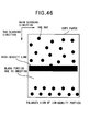
- Fig. 46 is an enlarged view of a low-density portion.
- a high-density line or character is present in an even low-density portion, no dots are formed after the line or character (the above-mentioned sweeping) (the arrow indicates the point of interest).
- Fig. 47 is an enlarged view of a high-density portion.
- a unique texture is generated (the arrow indicates the point of interest).
- the present invention has been made in consideration of the above-mentioned problems, and has as its object to provide an image processing apparatus and method which are free from any problems such as sweeping, texture, and the like even when the number of gray levels of an image is decreased.
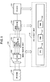
- Fig. 1 is a block diagram showing the arrangement of an image forming apparatus according to the first embodiment of the present invention.
- an image reading unit 109 is constituted by a CCD sensor 102, an analog signal processing unit 103, and the like, and an original image formed on the CCD sensor 102 via a lens 101 is converted into R (Red), G (Green), and B (Blue) analog electrical signals by the CCD sensor 102.
- the converted image signals are input to the analog signal processing unit 103, and are subjected to sample & hold processing, dark level correction, and the like in units of R, G, and B colors. Thereafter, the analog signals are analog-to-digital (A/D) converted into digital signals.
- A/D analog-to-digital
- the full-color signals thus digitized are input to an image processing unit 104.
- the image processing unit 104 performs correction processing required for the reading system such as shading correction, color correction, ⁇ correction, and the like, and other processing operations such as smoothing processing, edge emphasis, and the like, and outputs the processing result to a printer unit 105.
- the printer unit 105 is constituted by, e.g., an exposure control unit including a laser unit (not shown) and the like, an image forming unit, a feed control unit for a transfer paper sheet, and the like, and records an input image signal on a transfer paper sheet as an image.
- a CPU circuit unit 110 shown in Fig. 1 is constituted by a CPU 106, a ROM 107, a RAM 108, and the like, and systematically controls the sequence of the apparatus of this embodiment by controlling the image reading unit 109, the image processing unit 104, the printer unit 105, and the like.
- the image processing unit 104 shown in Fig. 1 will be described below.
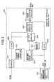
- Fig. 2 is a block diagram showing the arrangement of the image processing unit 104.
- digital image signals output from the analog signal processing unit 103 shown in Fig. 1 are input to a shading correction circuit unit 201.
- the shading correction circuit unit 201 corrects variations of sensors that read an original image, and the light distribution characteristics of a lamp for illuminating an original.
- the corrected image signals are input to a gradation correction unit 202 to be converted from luminance signals into density data, thus generating density image data.
- the image signals converted into density data are input to a color/monochrome conversion unit 203 which outputs monochrome data.
- the monochrome data output from the color/monochrome conversion unit 203 are input to a gradation conversion processing unit 204, and are subjected to error diffusion processing (density preservation type quantization processing) to attain pseudo halftone expression.
- error diffusion processing density preservation type quantization processing
- Y, M, and C data output from the gradation correction unit 202 are respectively subjected to the conversion processing in the gradation conversion processing unit 204.
- the gradation conversion processing unit will be described in detail below.
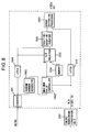
- Fig. 3 is a block diagram showing in detail the arrangement of the gradation conversion processing unit 204 according to the first embodiment.
- a counter 501 alternately generates timing signals of 0 and 1 at a 2-pixel period with reference to an Hsync signal.
- the timing signals output from the counter 501 are input to a random number generator 502, which generates a positive random number value only when the timing signal is 0.
- the signal output from the random number generator 502 is input to a maximum value controller 503 simultaneously with a signal (W/B) from the color/monochrome conversion unit 203.
- the maximum value controller 503 comprises a 255 ⁇ 255 ⁇ 8-bit look-up table, and controls the amplitude of an 8-bit signal from the random number generator 502 in accordance with an 8-bit signal from the color/monochrome conversion unit 203.
- the maximum value controller 503 performs output control to forcibly decrease the 8-bit signal value input from the random number generator 502.
- the maximum value controller 503 performs output control to amplify the 8-bit signal value input from the random number generator 502.
- the upper limit value of amplification of the signal value from the random number generator 502 is determined using an arbitrary value.
- Fig. 4 is a view showing the concept of the table arrangement of the maximum value controller 503.
- Fig. 4 shows the state wherein 8-bit output values are written in a matrix memory. That is, the matrix memory receives an 8-bit signal from the color/monochrome conversion unit 203 and an 8-bit signal from the random number generator 502, and outputs a memory value at the coordinate position defined by the two signals. Note that an input A of a selector 505 receives data from a memory 504, and an input A ⁇ thereof receives data from the maximum value controller 503.
- the signal output from the maximum value controller 503 with the above arrangement is input to the memory 504 and the selector 505.
- the memory 504 temporarily stores the 8-bit signal value.
- the selector 505 switches its inputs A and A ⁇ on the basis of the signal from the counter 501, which is synchronized with the timing of the maximum value controller 503, and outputs the input signal value.
- the selector 505 when the signal from the counter 501 is 0, the selector 505 directly outputs the signal from the maximum value controller 503; when the signal from the counter 501 is 1, the selector 505 outputs the signal from the memory 504. With this arrangement, an identical signal value can be output for two consecutive pixels.
- the signal value output from the selector 505 is input to a positive/negative inverter 506.
- the positive/negative inverter 506 performs control to switch the algebraic sign of the signal value input from the selector 505 to positive or negative on the basis of the timing signal from the counter 501. For example, when the signal value from the counter 501 is 0, the inverter 506 directly outputs the signal value from the selector 505 while leaving it "plus”; when the signal value from the counter 501 is 1, the inverter 506 inverts the sign of the signal value from the selector 505 to "minus", and outputs the inverted signal value.
- the signal value output from the positive/negative inverter 506 is added to a VIDEO signal output from the color/monochrome conversion unit 203, which has been timing-corrected in a latch 510, by an adder 507, and the sum is input to an error diffusion processor 508.
- an error diffusion processor 508 performs processing based on a normal 1-bit error diffusion method, though a detailed description thereof will be omitted.
- the number of bits of the error diffusion processing is not limited to 1 bit, but error diffusion processing to 2 to 4 bits may be performed.
- the error diffusion processor 508 diffuses errors generated upon conversion of m-bit input data into n-bit output data (m and n are integers and m > n) to surrounding input data by multiplying them with predetermined weighting coefficients.
- the VIDEO signal subjected to the above-mentioned processing is output from the image processing unit 104, and is finally output from the printer unit 105.
- the signal value of the random number generator is controlled in accordance with the input VIDEO signal value. That is, in a high-density portion, a normal random number is added to the VIDEO signal value while changing its sign to positive or negative. In a low-density portion, since granularity is conspicuous, a random number is added to the VIDEO signal value while gradually suppressing the amplitude of the random number and changing its sign to positive or negative as the density changes from high density to low density. In this manner, the granularity of images can be suppressed in consideration of the visual characteristics.
- Fig. 5 is a block diagram showing the arrangement of the gradation conversion processing unit according to a modification of the gradation conversion processing unit 204 according to the first embodiment shown in Fig. 3. Note that the same reference numerals in Fig. 5 denote the same parts as in Fig. 3, and a detailed description thereof will be omitted.
- a signal output from the color/monochrome conversion unit 203 is also input to an edge detector 511.
- the signal from color/monochrome conversion unit 203 is input to the maximum value controller 503 simultaneously with the signal output from the random number generator 502 and the signal output from the edge detector 511.
- the maximum value controller 503 controls the amplitude of an 8-bit signal from the random number generator 502 in accordance with an 8-bit signal from the color/monochrome conversion unit 203 and the signal from the edge detector 511.
- the 8-bit signal value input from the random number generator 502 is controlled to be forcibly decreased and output, independently of the magnitude of the 8-bit signal value input from the color/monochrome conversion unit 203.
- the signal value of the random number generator is controlled in accordance with edge information of the input VIDEO signal so as not to decrease the edge information by adding a random number to an edge portion of a thin line, a character, or the like, the edge information of input image information can be held, and an increase in granularity can be suppressed.
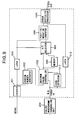
- Fig. 6 is a block diagram showing the arrangement of a gradation conversion processing unit according to the second embodiment.
- a counter 901 generates timing signals of 0, 1, and 2 in turn at a 3-pixel period with reference to an Hsync signal.
- the timing signal output from the counter 901 is input to a random number generator 902, which generates a positive random number only when the timing signal is 0.
- the signal output from the random number generator 902 is input to a maximum value controller 503 simultaneously with the signal from a color/monochrome conversion unit 203.
- the maximum value controller 503 performs the same processing as in the first embodiment, and thereafter, outputs the obtained signal value to a selector 903.
- the selector 903 performs processing for switching three signal values in accordance with the timing signal from the counter 901, which has been timing-corrected in a latch 509.
- the three signals are a signal having data value 0, the signal from the maximum value controller 503, and the signal from a memory 504.
- the selector 903 directly outputs the signal from the maximum value controller 503; when the switching signal is 1, the selector 903 outputs the signal from the memory 504; and when the switching signal is 2, the selector 903 outputs the value 0.
- the signal output from the selector 903 is input to a positive/negative inverter 904, and its sign is switched to positive/negative/0 in accordance with the timing signal from the counter 901. More specifically, when the signal value from the counter 901 is 0 or 2, the inverter 904 directly outputs the signal value from the selector 903 while leaving it "plus”; when the signal value from the counter 901 is 1, the inverter 904 inverts the sign of the signal value from the selector 903 to "minus" and outputs the inverted signal value.
- the signal value output from the positive/negative inverter 904 is processed in the same manner as in the first embodiment, and the processed signal is output from an error diffusion processor 508.
- the VIDEO signal subjected to the above-mentioned processing is output from an image processing unit 104, and is finally output from a printer unit 105.
- Fig. 7 is a block diagram showing the arrangement of the gradation conversion processing unit according to a modification of the second embodiment. As shown in Fig. 7, in the gradation conversion processing unit according to this modification, an edge detector 911 is added to the gradation conversion processing unit shown in Fig. 6.
- the signal output from the random number generator 902 is input to the maximum value controller 503 simultaneously with the signal from the color/monochrome conversion unit 203 and the signal from the edge detector 911.
- Fig. 8 is a block diagram showing the arrangement of a gradation conversion processing unit according to the third embodiment.
- a maximum value controller 1002 comprises a 255 ⁇ 255 ⁇ 8-bit look-up table as in the first embodiment, and controls the amplitude of an 8-bit signal from a random number generator 502 in accordance with an 8-bit signal from a color/monochrome conversion unit 203.
- the maximum value controller 1002 performs output control to forcibly decrease the 8-bit signal value input from the random number generator 502.
- the maximum value controller 1002 performs output control to amplify the 8-bit signal value input from the random number generator 502.
- the point which differentiates the maximum value controller 1002 according to the third embodiment from the maximum value controller of the first embodiment is that the amplification limit value of the output signal value is set to be a value equal to or smaller than a value twice as large as a level of a first threshold value of an error diffusion processor 1001.
- the signal value subjected to the same processing as in the first embodiment, as described above, is output from a positive/negative inverter 506, and is input to the error diffusion processor 1001 simultaneously with the signal from the color/monochrome conversion unit 203, which has been timing-corrected in a latch 510.
- This error diffusion processor 1001 performs processing for adding the signal value input from the positive/negative inverter 506 to a threshold value for an n-value conversion, although not shown.
- the signal value output from the error diffusion processor 1001 is output from an image processing unit 104, and is finally output from a printer unit 105.
- the processed random number is added to a threshold value for the n-value conversion in accordance with the ED method, the granularity of an image can be suppressed in consideration of the visual characteristics.
- Fig. 9 is a block diagram showing the arrangement of the gradation conversion processing unit according to a modification of the third embodiment. As shown in
- an edge detector 1011 is added to the gradation conversion processing unit shown in Fig. 8.
- the 8-bit signal value input from the random number generator 502 is controlled to be forcibly decreased and output, independently of the magnitude of the 8-bit signal value input from the color/monochrome conversion unit 203.
- the signal value of the random number generator is controlled in accordance with edge information of the input VIDEO signal, the edge information of input image information can be held, and an increase in granularity can be suppressed.
- Fig. 10 is a block diagram showing the arrangement of a gradation conversion processing unit according to the fourth embodiment.
- a maximum value controller 1102 comprises a 255 ⁇ 255 ⁇ 8-bit look-up table as in the second embodiment, and controls the amplitude of an 8-bit signal from a random number generator 902 in accordance with an 8-bit signal from a color/monochrome conversion unit 203.
- the amplification limit value of the output signal value is set to be a value equal to or smaller than a value twice as large as a level of a first threshold value of an error diffusion processor 1101.
- the signal value obtained as a result of the same processing as in the second embodiment is output from a positive/negative inverter 904, and is input to the error diffusion processor 1101 simultaneously with the signal from the color/monochrome conversion unit 203, which has been timing-corrected in a latch 510.
- This error diffusion processor 1101 performs processing for adding the signal value input from the positive/negative inverter 904 to a threshold value for an n-value conversion, although not shown.
- the signal value output from the error diffusion processor 1101 is output from an image processing unit 104, and is finally output from a printer unit 105.
- the processed random number is added to a threshold value of the n-value conversion, the same effect obtained upon adding the processed random value to the VIDEO signal is obtained, i.e., texture patterns generated upon n-value conversion processing tend to be connected vertically, thus allowing image formation which is stable in terms of the process.
- Fig. 11 is a block diagram showing the arrangement of the gradation conversion processing unit according to a modification of the fourth embodiment. As shown in Fig. 11, in the gradation conversion processing unit according to this modification, an edge detector 1111 is added to the gradation conversion processing unit shown in Fig. 10.
- the amplitude of an 8-bit signal from the random number generator 902 is controlled in accordance with an 8-bit signal from the color/monochrome conversion unit 203 and a signal from the edge detector 1111.
- the 8-bit signal value input from the random number generator 902 is controlled to be forcibly decreased and output, independently of the magnitude of the 8-bit signal value input from the color/monochrome conversion unit 203.
- the edge information of the original image can be preserved.
- Figs. 12 and 13 show the gradation conversion processing results according to the above embodiments and their modifications.
- Fig. 12 shows an output image obtained when a high-density line or character is present in an even low-density portion.
- Fig. 13 shows an output image obtained when an even middle-density portion is subjected to an ED processing.
- problems such as sweeping, texture, and the like can be solved by applying the present invention to the gradation conversion processing.
- the problems such as sweeping, texture, and the like can be solved without emphasizing the granularity of an image.
- Addition of a random number generated based on edge information which is detected from input image information to the input image information solves the problems such as sweeping, texture, and the like, without emphasizing the granularity of an image, while preserving the edge information.
- the maximum value controller comprises a look-up table, as described above.
- the present invention is not limited to such specific arrangement.
- the maximum value controller may comprise a logic arithmetic circuit.
- the fifth to eighth embodiments to be described below show, an example that can remove sweeping and texture as problems unique to the ED method or screen method without emphasizing granularity.
- the example described below can also solve the problem of a pseudo edge, and suppress moire.
- Fig. 14 is a block diagram showing in detail a gradation conversion processing unit 204 as the characteristic feature of this embodiment.
- the gradation conversion processing unit 204 shown in Fig. 14 alternately generates timing signals of 0 and 1 at a 2-pixel period using a counter 1301.
- the counter 1301 generates a signal in synchronism with each pixel of an image, and generates 0 at an edge portion.
- the timing signal output from the counter 1301 is input to a random number generator 1302, which generates a positive random number only when the timing signal is 0.
- the signal output from the random number generator 1302 is input to a random number sign controller 1303, in which its sign is randomly converted to positive or negative one, and the converted signal is output.
- the signal value output from the random number sign controller 1303 is input to an amplitude controller 1304, which controls the amplitude of that value in accordance with an 8-bit signal output from a color/monochrome conversion unit 203. More specifically, the output signal value from the controller 1304 acts as a function of the signal from the color/monochrome conversion unit 203, and the amplitude of the output signal is controlled to be decreased in low- and high-density portions with respect to density data.
- Fig. 18 shows an example of this amplitude control. An illustration denoted (a) in Fig. 18 shows a case wherein no amplitude control is performed, and an illustration (b) in Fig. 18 shows a case wherein the amplitude control is performed. That is, in (b), by controlling the amplitude, the function which acts to decrease the amplitudes of random values in the low- and high-density portions is applied.
- the signal output from the amplitude controller 1304 is input to a memory 1305 and a selector 1307.
- the memory 1305 temporarily stores the signal value output from the amplitude controller 1304.
- the selector 1307 switches inputs A and A ⁇ on the basis of the signal from the counter 1301. When the signal from the counter 1301 is 0, the selector 1307 directly outputs the signal output from the amplitude controller 1304; when the signal from the counter 1301 is 1, the selector 1307 outputs the signal output from a sign inverter 1306.
- the sign inverter 1306 outputs the signal from the memory 1305 while inverting its sign.
- the inverter 1306 when data from the memory 1305 has the negative sign, the inverter 1306 inverts the sign to the positive one and outputs the inverted data; when data from the memory 1305 has the positive sign, the inverter 1306 inverts the sign to the negative one and outputs the inverted data.
- a pair of positive and negative or negative and positive random number values having equal absolute values can be output for two consecutive pixels.
- the signal value output from the selector 1307 is added to a VIDEO signal output from the color/monochrome conversion unit 203 by an adder 1309, and the sum signal is input to an error diffusion processor 1308.
- an error diffusion processor 1308 performs processing based on normal error diffusion for binary data, screen processing such as dithering for binary data, or the like, although its details are not shown.
- the VIDEO signal subjected to the above-mentioned processing is output from an image processing unit 104 shown in Fig. 1, and is finally output from a printer unit 105.
- the signal value output from the random number generator is controlled to be a function of the VIDEO signal value, as shown in the illustration (b) in Fig. 18.
- sweeping and texture as the problems unique to the n-bit ED method or screen method can be removed without emphasizing granularity, the problem of a pseudo edge can also be solved, and moiré can be suppressed.
- the signs of random number values are randomly switched in the order from positive to negative or from negative to positive in units of two pixels.
- the present invention is not limited to the two-pixel system, but the signs may be switched in units of three pixels. In this case, the signs of random number values may be randomly switched in the order of (positive, 0, negative) or (negative, 0, positive).
- Fig. 15 is a block diagram showing in detail the arrangement of a gradation conversion processing unit 204 of the sixth embodiment.
- a signal value output from a random number sign controller 1303 is input to a memory 1305 and a selector 1307.
- the memory 1305 temporarily stores the signal value output from the random number sign controller 1303 as in the fifth embodiment.
- the selector 1307 switches inputs A and A ⁇ on the basis of the signal from a counter 1301. More specifically, when the signal from the counter 1301 is 0, the selector 1307 directly outputs the signal from the random number sign controller 1303; when the signal from the counter 1301 is 1, the selector 1307 outputs the signal from a sign inverter 1306.
- the sign inverter 1306 outputs the signal from the memory 1305 while inverting its sign as in the fifth embodiment.
- the inverter 1306 inverts the sign to positive and outputs the inverted data; when data from the memory 1305 has the positive sign, the inverter 1306 inverts the sign to negative and outputs the inverted data.
- the signal output from the selector 1307 is input to an amplitude controller 1304, and the ratio of the amplitude of a random number is controlled in units of pixels, as shown in the illustration (b) in Fig. 18. Thereafter, the amplitude-controlled signal is output.
- the signal value output from the amplitude controller 1304 is added to a VIDEO signal from a color/monochrome conversion unit 203, by an adder 1309, and the sum signal is input to an error diffusion processor 1308. Then, the signal is subjected to processing such as normal n-bit error diffusion, screen processing, or the like.
- the VIDEO signal subjected to the above-mentioned processing is output from an image processing unit 104 shown in Fig. 1, and is finally output from a printer unit 105.
- the amplitude control by the amplitude controller 1304 is performed on each pixel, which does not result in adding random number values having equal absolute values but different signs to odd- and even-numbered pixels, and hence, density data cannot be accurately preserved, as compared to the fifth embodiment.
- it is capable of controlling not to add unnecessary data to the edge of a character portion or an image portion, and the reproducibility of the edge portion can be improved.
- Fig. 16 is a block diagram showing in detail a gradation conversion processing unit 204 according to the seventh embodiment.
- a counter 1301 alternately generates timing signals of 0 and 1 at a two-pixel period as in the fifth embodiment.
- the counter 1301 generates a signal in synchronism with each pixel of an image, and generates 0 at an edge portion.
- the timing signal from the counter 1301 is input to a random number generator 1501, which generates a random number only when the timing signal is 0.
- the signal output from the random number generator 1501 is a random number value that has either the positive or negative sign.
- the signal from the random number generator 1501 is input to a memory 1305 and a selector 1307.
- the selector 1307 selects and outputs one of the signal value from the random number generator 1501 and a signal from a sign inverter 1306, which are inputs at terminals A and A ⁇ of the selector 1307, on the basis of the signal from the counter 1301.
- the sign inverter 1306 outputs the signal from the memory 1305 while inverting its sign, as in the fifth embodiment.
- the signal value output from the selector 1307 is added to a VIDEO signal from a color/monochrome conversion unit 203 by an adder 1309, and the sum signal is input to an error diffusion processor 1308. Then, the signal is subjected to processing such as normal n-bit error diffusion, screen processing, or the like.
- the VIDEO signal subjected to the above-mentioned processing is output from an image processing unit 104 shown in Fig. 1, and is finally output from a printer unit 105.
- a random number sign controller 1306 can be omitted, and the hardware arrangement can be simplified, as compared to the fifth embodiment.
- Fig. 17 is a block diagram showing in detail a gradation conversion processing unit 204 according to the eighth embodiment.
- a counter 1301 alternately generates timing signals of 0 and 1 at a two-pixel period as in the fifth embodiment.
- the timing signal from the counter 1301 is input to a random number generator 1501, which generates a random number only when the timing signal is 0.
- the signal output from the random number generator 1501 is a random number which may have either the positive or negative sign, as in the seventh embodiment.
- the signal value from the random number generator 1501 is input to a memory 1305 and a selector 1307.
- the selector 1307 selects and outputs signal values which are inputs at its terminals A and A ⁇ , on the basis of the signal from the counter 1301. More specifically, when the signal from the counter 1301 is 0, the selector 1307 directly outputs the signal from the random number generator 1501; when the signal from the counter 1301 is 1, the selector 1307 outputs a signal from a sign inverter 1306.
- the sign inverter 1306 outputs the signal from the memory 1305 while inverting its sign, as in the fifth embodiment. With this arrangement, random number values having equal absolute values but different signs can be output for two consecutive pixels.
- the signal from the selector 1307 is input to an amplitude controller 1304, and the ratio of the amplitude of a random number is controlled in units of pixels, as shown in the illustration (b) in Fig. 18. Thereafter, the amplitude-controlled signal is output.
- the signal value output from the amplitude controller 1304 is added to a VIDEO signal from a color/monochrome conversion unit 203 by an adder 1309, and the sum signal is input to an error diffusion processor 1308. Then, the signal is subjected to processing such as normal n-bit error diffusion, screen processing, or the like.
- the VIDEO signal subjected to the above-mentioned processing is output from an image processing unit 104 shown in Fig. 1, and is finally output from a printer unit 105.
- the amplitude controller 1304 since the amplitude controller 1304 performs amplitude control on each pixel as in the sixth embodiment, density data cannot be accurately preserved as compared to the fifth embodiment. However, it is possible to perform control that does not add unnecessary data to the edge of a character portion or an image portion, and the reproducibility of the edge portion can be improved.
- the random number generator 1501 since the random number generator 1501 generates random numbers having both the positive and negative signs, a random number sign controller can be omitted, and the hardware arrangement can be simplified.
- an image processing apparatus comprises a random number generation means for generating positive random number values at every other pixel, a random number sign control means for randomly converting the signs of the random number values generated by the random number generation means to positive or negative, an amplitude control means for changing the ratio of the amplitude of each of the random number values output from the random number sign control means as a function of a signal value of input image data, a sign inversion means for generating at a pixel position where no random number value is generated by the random number generation means, a value which has the same absolute value as but a different sign from a value output from the amplitude control means at an immediately preceding pixel position, and an addition means for alternately adding the signal values generated by the amplitude control means and the sign inversion means to signal values of the input image data.
- the image processing apparatus is characterized in that moiré can be suppressed while solving the problem associated with granularity that worsens upon adding a random number to normal image density data.
- This invention is not limited to an image formation in which gradation conversion from 8 bits to 1 bit is performed. It is also characterized remove switching noise, i.e., a pseudo edge generated when performing gradation conversion to other gray levels (e.g., n bits such as 2 bits, 3 bits, and the like).
- sweeping and texture as the problems unique to the n-bit ED method or screen method can be removed without emphasizing granularity, and the problem of a pseudo edge can also be solved, and moiré can be suppressed.
- Fig. 19 is a block diagram showing in detail a gradation conversion processing unit 204 as the characteristic feature of the ninth embodiment.
- a random number adder 1401 adds a random number to input image data (8 bits, 256 levels).
- Figs. 20, 21, and 22 are explanatory views of the random number adder 1401.
- reference numerals 1501, 1502, and 1504 denote flip-flops; 1503 and 1506, EX-OR gates; 1509, a multiplier; 1510, an AND gate; 1505 and 1508, random number generators; 1507, a sign generator; and 1511, an adder.
- Hsync and Video clock (Video CK) signals generated in the main scanning direction (X-direction) are respectively input to the flip-flops 1501 and 1502, which generate signals at timings of signals sigl and sigl' shown in Fig. 21.
- the sigl represents a signal generated in an even line
- the sigl' represents a signal generated in an odd line.
- the signals sigl and sigl' shown in Fig. 21 correspond to signals generated in portions of "+, -, -, +, -, ... " shown in Fig. 20.
- signals are two-dimensionally generated in a checkerboard pattern by shifting the generation positions by one pixel in the first and second lines.
- the signal output from the EX-OR gate 1503 is input as a timing signal to the random number generators 1505 and 1508 via the flip-flop 1504 at timings of signals sig2 and sig2' shown in Fig. 21.
- signals are generated on the left side of circled portions shown in Fig. 20. That is, signals are generated every four pixels in an even line, and in an odd line, signals are generated every four pixels at positions shifted by one pixel from those generated in the even line. Therefore, the random number generator 1 (1508) generates a random number ranging from 0 to 31 every four pixels in synchronism with the signal from the flip-flop 1504.
- the random number value from the generator 1508 is multiplied with a signal from the sign generator 1507 by the multiplier 1509.
- the random number generator 2 (1505) generates a random number of 0 or 1 every four pixels in synchronism with the signal from the flip-flop 1504 as in the random number generator 1 (1508).
- the signal value output from the generator 1505 is EX-ORed with a signal from the flip-flop 1504 by the EX-OR gate 1506, and the result is input to the sign generator 1507.
- the random number adder 1401 can generate pairs of positive and negative or negative and positive random numbers at every other positions in a checkerboard pattern while shifting the generation positions by one pixel with respect to even and odd lines, as shown in Fig. 20, by calculating the output signals from the sign generator 1507 and the random number generator 1508 by the multiplier 1509.
- the random value obtained from the multiplier 1509 is added to a Video signal by the adder 1511 in accordance with the signal from the EX-OR gate 1503, only when no character signal is input. That is, when a character signal representing a character portion is input as a Video signal, no random number is added, while only when values of the Video signal do not represent a character portion, random numbers are added to the values of the Video signal at every other positions in a checkerboard pattern.
- the arrangement for adding positive and negative (or negative and positive) random numbers at every other pixel positions can suppress granular noise since the number of pixels using random numbers is small.
- each of the random number generators 1505 and 1508 comprises an m-sequence shift register code sequence generator. With this generator, when the number of stages of the shift register is set to be N, pseudo random numbers having a period of 2N - 1 can be easily generated by a simple hardware arrangement.
- Each generator according to this embodiment comprises a 25-stage, 1-bit shift register so as to prevent generation of periodicity even when an A3 original is processed at 400 dpi.
- random number (p[16]*32 + p[17]*16 + p[18]*8 + p[19]*4 + p[20]*2 + p[21]*16/63
- the signal output from the random number adder 1401 is density-corrected by an error adder 1402 using correction signals from a binarization unit 1406 and an error RAM 1407.
- Figs. 24 and 25 show the details of the error adder 1402. Referring to Fig.
- reference numerals 1706, 1712, 1713, 1714, 1715, 1716, 1721, and 1726 denote latch circuits; 1707, 1708, 1709, 1710, 1711, 1722, and 1723, multipliers; 1717, 1718, 1719, 1720, 1724, 1725, 1702, and 1705, adders and subtracters; 1701, a constant adder for adding a constant "255"; and 1703 and 1704, arithmetic devices.
- Signals from the error RAM 1407 and the binarization unit 1406 are input to the latches 1706 and 1721, for calculating accumulated error. Thereafter, the subtraction processing is performed on the accumulated error with respect to a signal value from the constant adder 1701 by the subtracter 1702.
- the signal from the constant adder 1701 is obtained by adding "+255" to an input Video signal so as for the output to become a negative value. With this calculation, the amplitude of the Video signal falls within the range from 0 to 510.
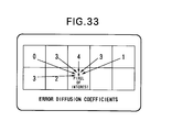
- the multipliers 1707, 1708, 1709, 1710, and 1711 for obtaining the accumulated error use coefficients "0, 3, 4, 3, 1" shown in Fig. 24.
- the multipliers 1722 and 1723 use coefficients "4, 2" shown in Fig. 24. These coefficients are characterized in that their sum is 17. That is, the sum total of the weighting coefficients is 17.
- the signal output from the subtracter 1702 is divided by a constant "17" by the arithmetic device 1703. Then, the error adder 1402 outputs the result (quotient: 0 to 30) as an upper 5-bit signal bufH, and outputs the remainder (0 to 16) as a lower 5-bit signal bufL.
- the characteristic feature of this arrangement is as follows.
- the quotient bufH falls within the range from 0 to 30.
- the division in the arithmetic device that calculates the accumulated error can be omitted, and the number of bits of the input signal to the arithmetic device 1703 can be reduced, thus reducing the memory capacity of the error RAM 1407 shown in Fig. 19.
- the density of the Video signal can be preserved.
- the ninth embodiment is characterized by using a mask having substantially the same error diffusion coefficients, the sum total of which is 17, when a character signal is input.
- the lower 5-bit signal bufL output from the error adder 1402 is input to a comparator 1403, and is compared with a signal (0 to 16) from a random number generator 1404. If the signal value bufL is larger than the signal from the random number generator 1404, the comparator 1403 generates a BL signal "1"; otherwise, the comparator 1403 generates a BL signal "0". Not that the hardware arrangement of the random number generator 1404 is the same as that shown in Fig. 23, and a detailed description thereof will be omitted.
- the adder 1405 outputs a result obtained by adding the upper 5-bit signal bufH from the error adder 1402 and the BL signal from the comparator 1403, and by subtracting a constant "15" from the sum, to the binarization unit 1406.
- the value "17” in the division 255/17 is obtained from " ⁇ 17" used in the arithmetic device 1703 within the error adder 1402.
- the binarization unit 1406 determines only if the input value is larger or smaller than a threshold value "0". If the input data is larger than the threshold value "0", the unit 1406 outputs "1" to hold the generated 4-bit quantization error in a memory. At this time, the quantization error is calculated by "input data - 15". On the other hand, when the input data value is smaller than the threshold value "0", the unit 1406 outputs "0" to similarly hold the generated 4-bit quantization error in the memory. In the latter, the quantization error is calculated by "input data - 0".
- This arrangement is characterized in that the error value calculated by decreasing the number of bits is held in the memory, and the corrected signal value subjected to the accumulated error calculation is fed back to the error adder 1402 at the input stage of the section that processes a multi-value signal in the gradation conversion processing unit.
- the signal value subjected to the above-mentioned processing is output as a VIDEO signal from an image processing unit 104 shown in Fig. 1, and is finally output from a printer unit 105.
- the comparator 1403 shown in Fig. 19 attains binarization by comparing the signal bufL from the error adder 1402 and the signal from the random number generator 1404.
- the same processing can be attained by replacing the circuit of the random number generator 1404 by a dither generation circuit 1801 shown in Fig. 26. More specifically, a pattern ranging from 0 to 16 is generated by the dither generation circuit, and compares it with the signal bufL from the error adder 1402, thus attaining binarization.
- the ninth embodiment by generating random number values whose maximum values are controlled at intervals of several pixels with respect to the input Video signal values, and by adding random pairs of positive and negative or negative and positive random number values having equal absolute values to the Video signal values at intervals of several pixels, the problems of sweeping and texture can be solved while suppressing granular noise.
- the conventional error diffusion method requires a sufficiently large memory capacity which causes to raise a cost, so as to hold errors generated upon quantization.
- pseudo halftone processing of L level is performed, by setting the quotient and remainder, which are obtained by dividing an input video signal by an arbitrary constant, respectively to be upper- and lower-bit signals, binarization is performed by comparing it with a random number or a dither signal, and errors generated as a result of error diffusion processing of the pseudo halftone signal of the L level are corrected as accumulated errors of neighboring pixels with respect to the input video signal.
- the number of bits required by the memory for holding errors can be decreased, and a cost reduction can also be attained.
- random numbers are generated every four pixels, and the signs of the random numbers are inverted every other pixels.
- this processing amounts to generating random numbers every 2 ⁇ + 1 pixels ( ⁇ is integer; ⁇ > 0) and inverting the signs of the random numbers every ⁇ pixels.
- Fig. 27 is a block diagram showing in detail a gradation conversion processing unit 204 of the 10th embodiment. In Fig. 27, this embodiment is different from the ninth embodiment in a portion of a random number adder 1901. Figs. 28 to 31 are views for explaining the details of the random number adder 1901.
- symbols "+” and “-" represent pixels to which random numbers are to be added. That is, positive random numbers are added at the positions indicated by the symbols "+”, and negative random numbers are added at the positions indicated by the symbols "-”.
- pairs of random numbers in circled portions are controlled to have equal absolute values, and are added to Video signal values. That is, this embodiment is characterized in that random pairs of positive and negative or negative and positive random numbers are added to Video signal values.
- the same effect as in the ninth embodiment can be obtained not only by adding random numbers in a checkerboard pattern shown in Fig. 20 but also by adding random numbers at positions every three pixels, every four pixels, and the like in patterns shown in Figs. 28, 30, and 31.
- the 10th embodiment by decreasing the number of pixels to which random numbers are to be added with respect to a Video signal, granular noise can be reduced.
- the hardware arrangements for realizing the addition patterns shown in Figs. 28 to 31 can be constituted based on the same concept as that of the arrangement of the ninth embodiment shown in Fig. 22, and a detailed description thereof will be omitted.
- the signal value subjected to the above-mentioned processing is also subjected to the same processing as in the ninth embodiment, and is output from an image processing unit 104 (Fig. 1) as a 1-bit Video signal.
- the video signal is then output from a printer unit 105.
- the problems of sweeping and a pseudo edge can be solved without emphasizing granular noise.
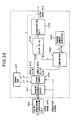
- Fig. 32 is a block diagram showing in detail a gradation conversion processing unit of the 11th embodiment. In Fig. 32, this embodiment is different from the ninth and 10th embodiments in a portion of an error adder 2101. Figs. 33 and 34 are views for explaining the details of the error adder 2101.
- this embodiment has a difference point compared with the ninth embodiment that the division by a constant "16" is replaced by the division by the constant "17". That is, arithmetic devices 2201 and 2202 can be attained by a simple bit shifting. According to this arrangement, a complicated calculation can be omitted, thus simplifying the hardware arrangement.
- an upper-bit signal bufH output from the error adder 2101 in Fig. 32 consists of 5 bits that can express a value ranging from 0 to 31, and a lower-bit signal bufL consists of 4 bits that can express a value ranging from 0 to 15.
- bufH may be assumed to be 32.
- the division in the arithmetic device that calculates an accumulated error can be omitted, and at the same time the hardware arrangement can be simplified. Also, the number of bits contained in the input signal to the arithmetic device 2201 can be reduced, and hence, the memory capacity of an error RAM 1407 can be reduced.
- the signal value subjected to the above-mentioned processing is also subjected to the same processing as in the ninth embodiment, and is output from an image processing unit 104 (Fig. 1) as a 1-bit Video signal.
- the video signal is then output from a printer unit 105.
- the 11th embodiment can simplify the hardware arrangement compared to the ninth embodiment, since the hardware arrangement of the arithmetic device 2201 can be realized only by bit shifting.
- binarization has been exemplified. That is, the binarization unit 1406 shown in each of Figs. 19, 26, 27, and 32 performs binarization.
- the present invention is not limited to binarization, but may be similarly applied to n-value conversion processing (n is an integer which is larger than 2).
- an error diffusion method is used.
- the present invention is not limited to the processing using the error diffusion, and the same effect can be expected even when the binarization unit is replaced by one that performs dither processing, screen processing, or the like.
- binarization is performed after upper and lower bits are separated.
- the present invention is not limited to this specific arrangement.
- the random-number addition method of the present invention can also be applied to the arrangement that simply performs n-value (n is an integer equal to or larger than 2) conversion processing without separating upper and lower bits.
- the upper-bit signal bufH consists of 5 bits.
- the present invention is not limited to this specific number of bits.
- the number of bits of the upper-bit signal bufH may be 3 or 4.
- Constant values the signs of which are switched randomly (using random numbers) in pairs of positive and negative values or negative and positive values, are amplitude-controlled in accordance with the input image signal values, and are added to the input image signal.
- Random number values which are amplitude-controlled in accordance with the input image signal values, are added to the input image signal by inverting their signs in the order of positive and negative at predetermined periods.
- Random number values the signs of which are switched randomly (using random numbers) in pairs of positive and negative values or negative and positive values, are amplitude-controlled in accordance with the input image signal values, and are added to the input image signal.
- the ninth, 10th, and 11th embodiments by generating random number values whose maximum values are controlled at intervals of several pixels with respect to the input video signal values, and by adding random pairs of positive and negative or negative and positive random number values having equal absolute values to the video signal values at intervals of several pixels, the problems of sweeping and texture can be solved while suppressing granular noise.
- the image processing method and apparatus vary the generation period of pseudo random numbers to be added to an image signal in correspondence with the feature signal of image data. More specifically, for a flat portion, i.e., a pixel having a small edge amount, as shown in Fig. 35a, three density levels generated based on one pseudo random number are respectively reflected in image data of three pixels, as shown in Fig. 35c.
- a pseudo random number a is converted into pseudo random numbers +a/2 -a, and +a/2, and thereafter, these random numbers are added to corresponding three pixel data.
- a pseudo random number +a/2 is added to a pixel so as for the pixel value to be easily changed to logic level "1" upon error diffusion processing. More specifically, on a non-edge portion, dots that capable of being easily changed to logic level "1" can be controlled not to be isolated but to gather together, and on an edge portion, dots can be controlled to be scattered.
- the density can be preserved, and high image quality can be assured for both a smooth portion such as a photograph and a portion such as an edge in which the density abruptly changs.
- Fig. 37 shows the detailed arrangement of an image processing unit 204 according to the 12th embodiment.
- An image signal converted into a digital signal by an analog signal processing unit 203 is input to a shading correction circuit 2301.
- the shading correction circuit 2301 performs black correction and white correction processing.
- the output level, in a dark portion, of a CCD sensor becomes larger than the original one.
- the entire read image has higher luminance level than the original image. To prevent this, the output level of the CCD obtained when an exposure lamp is turned off is subtracted from the read image signal.
- the white level correction will be described below.
- a reference white plate set at the reference position is read, and variations of an illumination system, an optical system, and sensitivity of the sensor are corrected on the basis of the read white plate data.
- a density conversion gradation correction unit 2302 will be described below.
- the converted value Dout calculated by this equation, which corresponds to each input value Di is set in advance in the log conversion table.
- the log conversion table 2306 converts an input value Din into the corresponding value Dout, and outputs the converted value. This output is sent to a gradation correction table 2307.
- the gradation correction table 2307 will be described below.
- the gradation correction table 2307 corrects the gradation characteristics of an image output apparatus.
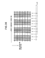
- Fig. 38 shows an example of the gradation characteristics of an electrophotographic printer.
- Fig. 38 shows the output printer density with respect to the input data value.
- Fig. 39 shows input/output characteristics to be set in the gradation correction table 2307 so as to correct the nonlinear input/output characteristics to linear characteristics.
- the gradation correction table 2307 pre-stores converted output values corresponding to different input data values so as to hold the input/output characteristics shown in Fig. 39.
- This gradation correction table 2307 receives the output value from the log conversion table 2306, and outputs a linearly converted output value.
- the edge discrimination unit 2303 will be described below with reference to Fig. 40.
- the edge discrimination unit 2303 comprises filters 2505 and 2506 for detecting primary differential signals.
- Each filter comprises, e.g., a 5 ⁇ 5 pixel matrix, as shown in Fig. 40.
- This filter 2505 performs processing for calculating the absolute value of the difference between the average value of the first and second lines and the average value of the fourth and fifth lines, with respect to signals (Video data) of five lines input in the sub-scanning direction.
- the filter 2506 performs processing for calculating the absolute value of the difference between the average values of the first and second pixels in the respective lines and the average value of the fourth and fifth pixels, with respect to signals (Video data) in five lines input in the main scanning direction.
- An image signal which has been converted into a predetermined density value by the log conversion table 2306 is delayed by a predetermined number of lines by delay FIFO memories 2501, 2502, 2503, and 2504 in the line direction, and thereafter, the absolute values of the density differences are calcuated by a filter 2505 for detecting density changes in the sub-scanning direction and a filter 2506 for detecting density changes in the main scanning direction. Then, the absolute values are added to each other by an adder 2507.
- a comparator 2508 compares the sum value with an arbitrary setting value, and a discrimination result is output.
- the edge amount when the edge amount is large, "1" is output as an edge detection signal; otherwise, "0" is output as an edge detection signal.
- the arbitrary setting value (threshold value) is set in a register 2509 via a CPU bus 2305 by a CPU 106 prior to read-out of an image.
- a gradation conversion processing unit 2304 will be described below with reference to Fig. 41. Since a printer used in the 12th embodiment is a binary printer, an input image signal must be converted into a binary signal. The gradation conversion processing unit 2304 performs such processing.
- An image signal that has been subjected to the density conversion and the gradation correction in the gradation correction unit 2302 is added to a pseudo random number whose period is variable, as one characteristic feature of the 12th embodiment, by an adder 2607, and the sum signal is then subjected to binarization processing in an error diffusion processor 2608.
- the pseudo random number to be added to image data is generated in synchronism with a pixel clock (to be referred to as a VCLK hereinafter) 2602.
- the input VCLK 2602 is frequency-divided to 1/3 VCLK by a frequency-division counter 2603, and the divided VCLK 2602 is input to a pseudo random number generator 2604.
- a pseudo random number generator 2605 receives the VCLK 2602 which is not frequency-divided.
- the pseudo random number generator 2604 generates the following data with respect to a pseudo random number generated in synchronism with the frequency-divided clock, 1/3 VCLK, in synchronism with the input clock, as shown in Figs. 35a and 35c: +a/2, -a, +a/2 This is for allowing an image to which the following value is distributed to be easily changed to logic level "1" in the subsequent error diffusion processor 2608, as shown in Fig. 36: "+pseudo random number value/2" By regularly neighboring pixels which can be easily changed to logic level "1", the granularity of an output image can be suppressed.
- Fig. 42 is a timing chart in which the period of a pseudo random number is variable in correspondence with the edge amount.
- Pseudo random number d'ata of level 1 is a pseudo random number value generated by the pseudo random number generator 2604
- a pseudo random number of level 2 is the one generated by the pseudo random number generator 2605.
- a selector 2606 selects the pseudo random number value of level 2 when the edge discrimination signal is "0"; it selects the pseudo random number of level 1 when the edge discrimination signal is "1".
- the selector 2606 outputs the selected random number to an adder 2607.
- the adder 2607 adds the input random number to image data, as described above, and the sum data is binarized by the error diffusion processor 2608.
- the binary data is supplied to a printer unit 105, thus performing image formation.
- the two pseudo random number generators 2604 and 2605 are used.
- Fig. 43 shows an arrangement using one pseudo random number generator 2610. Hence, pseudo random numbers having two different periods can be generated by a simple arrangement.
- Fig. 43 shows another arrangement of the gradation conversion processing unit of the 12th embodiment.
- the same reference numerals in Fig. 43 denote the same elements as in Fig. 41. Therefore, only portions different from those in Fig. 41 will be explained below.
- the unit of Fig. 43 realizes processing equivalent to the processing attained by the two pseudo random number generators 2604 and 2605 shown in Fig. 41, by using the pseudo random number generator 2610 and a D flip-flop 2611.
- the pseudo random number generator 2610 has the same arrangement as that of the pseudo random number generator 2605 shown in Fig. 41, and generates and outputs a pseudo uniform random number in synchronism with the input VCLK.
- the output from this generator 2610 is input to the selector 2606 and a data input terminal of the D flip-flop 2611.
- the D flip-flop 2611 latches pseudo random number data from the pseudo random number generator 2610 in synchronism with the clock from the frequency-division counter 2603, and outputs the latched data to the selector 2606.
- pseudo random number generators shown in Figs. 41 and 43 may comprise a sequence circuit or may be realized by executing a pseudo random number generation program by a microprocessor.
- error diffusion processor may comprise a sequence circuit, or may be realized by executing an error diffusion processing program by a microprocessor.
- the gradation conversion processing unit can be constituted by a simpler arrangement.
- texture peculiar to the density preservation method can be removed by adding a pseudo random number to image data, and a halftone image such as a photograph can be stably reproduced and a sharp image can be obtained at an edge portion by varying the period of random numbers.
- the present invention may be applied to either a system constituted by a plurality of equipments such as a FAX apparatus, a digital copying machine, a printer, and the like, or an apparatus consisting of a single equipment (e.g., a FAX apparatus, a digital copying machine, a printer, or the like).
- the present invention is also attained by describing the processing sequence of the image processing unit 104 represented by Fig. 1 above in a software manner, pre-storing the program in the ROM 107, and executing the program by the CPU.
- the objects of the present invention are also achieved by supplying a storage medium,'which records a program code of a software program that can realize the functions of the above-mentioned embodiments to the system or apparatus, and reading out and executing the program code stored in the storage medium by a computer (or a CPU, MPU, or the like) of the system or apparatus.
- the program code itself read out from the storage medium realizes the functions of the above-mentioned embodiments, and the storage medium which stores the program code constitutes the present invention.
- the storage medium for supplying the program code for example, a floppy disk, hard disk, optical disk, magneto-optical disk, CD-ROM, CD-R, magnetic tape, nonvolatile memory card, ROM, and the like may be used.
- the functions of the above-mentioned embodiment may be realized not only by executing the program code read out by the computer but also by some or all of actual processing operations executed by an OS (operating system) running on the computer on the basis of an instruction of the program code.
- OS operating system
- the functions of the above-mentioned embodiments may be realized by some or all of actual processing operations executed by a CPU or the like arranged in a function extension board or a function extension unit, which is inserted in or connected to the computer and receives the program code read out from the storage medium.
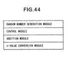
- the storage medium stores program codes corresponding to the above-mentioned image processing. These program codes will be briefly described below.
- the storage medium stores modules shown in an example of the memory map in Fig. 44. That is, the storage medium stores program codes of at least a random number generation module, a control module, an addition module, and an n-value conversion module.
Landscapes
- Engineering & Computer Science (AREA)
- Multimedia (AREA)
- Signal Processing (AREA)
- Image Processing (AREA)
- Facsimile Image Signal Circuits (AREA)
Applications Claiming Priority (12)
| Application Number | Priority Date | Filing Date | Title |
|---|---|---|---|
| JP33363095 | 1995-12-21 | ||
| JP33363095A JP3432064B2 (ja) | 1995-12-21 | 1995-12-21 | 画像処理装置及び方法 |
| JP333630/95 | 1995-12-21 | ||
| JP8076850A JPH09270914A (ja) | 1996-03-29 | 1996-03-29 | 画像処理方法とその装置 |
| JP76850/96 | 1996-03-29 | ||
| JP7685096 | 1996-03-29 | ||
| JP19080596A JP3428822B2 (ja) | 1996-07-19 | 1996-07-19 | 画像処理装置及び画像処理方法 |
| JP19080396A JP3461247B2 (ja) | 1996-07-19 | 1996-07-19 | 画像処理装置及び画像処理方法 |
| JP190805/96 | 1996-07-19 | ||
| JP19080596 | 1996-07-19 | ||
| JP190803/96 | 1996-07-19 | ||
| JP19080396 | 1996-07-19 |
Publications (3)
| Publication Number | Publication Date |
|---|---|
| EP0781034A2 true EP0781034A2 (fr) | 1997-06-25 |
| EP0781034A3 EP0781034A3 (fr) | 1998-08-05 |
| EP0781034B1 EP0781034B1 (fr) | 2004-03-24 |
Family
ID=27465976
Family Applications (1)
| Application Number | Title | Priority Date | Filing Date |
|---|---|---|---|
| EP96309371A Expired - Lifetime EP0781034B1 (fr) | 1995-12-21 | 1996-12-20 | Appareil et procédé de traitement d'images |
Country Status (3)
| Country | Link |
|---|---|
| US (1) | US5805738A (fr) |
| EP (1) | EP0781034B1 (fr) |
| DE (1) | DE69631948T2 (fr) |
Cited By (4)
| Publication number | Priority date | Publication date | Assignee | Title |
|---|---|---|---|---|
| EP0903932A2 (fr) * | 1997-09-23 | 1999-03-24 | Xerox Corporation | Système et procédé pour obtenir la sélection dynamique d'un profil de bruit pour le traitement d'images par diffusion d'erreurs hybride |
| EP1133162A2 (fr) * | 2000-03-07 | 2001-09-12 | Seiko Instruments Inc. | Procédé et dispositif pour la reproduction de gradation d'images à tons continus |
| EP1157840A2 (fr) * | 2000-05-22 | 2001-11-28 | Canon Kabushiki Kaisha | Compensation pour buses défectueuses |
| CN112231464A (zh) * | 2020-11-17 | 2021-01-15 | 安徽鸿程光电有限公司 | 信息处理方法、装置、设备及存储介质 |
Families Citing this family (17)
| Publication number | Priority date | Publication date | Assignee | Title |
|---|---|---|---|---|
| US6282323B1 (en) * | 1996-12-04 | 2001-08-28 | Canon Kabushiki Kaisha | Image processing method and apparatus |
| US6496256B1 (en) * | 1999-10-01 | 2002-12-17 | Applied Materials, Inc. | Inspection systems using sensor array and double threshold arrangement |
| JP2001136402A (ja) * | 1999-11-10 | 2001-05-18 | Minolta Co Ltd | 色変換装置 |
| US6614557B1 (en) * | 1999-12-07 | 2003-09-02 | Destiny Technology Corporation | Method for degrading grayscale images using error-diffusion based approaches |
| JP2002171410A (ja) * | 2000-12-01 | 2002-06-14 | Minolta Co Ltd | 画像処理装置 |
| US8009327B2 (en) * | 2002-07-11 | 2011-08-30 | Canon Kabushiki Kaisha | Method and apparatus for image processing |
| JP4531491B2 (ja) * | 2003-11-21 | 2010-08-25 | 株式会社リコー | 画像形成装置及び画像形成方法 |
| KR100499102B1 (ko) * | 2003-12-15 | 2005-07-01 | 엘지전자 주식회사 | 플라즈마 디스플레이 패널의 구동장치 및 구동방법 |
| JP4418713B2 (ja) * | 2004-06-11 | 2010-02-24 | キヤノン株式会社 | 乱数発生方法及び乱数発生装置 |
| US20060203280A1 (en) * | 2005-02-25 | 2006-09-14 | Matsushita Electric Industrial Co., Ltd. | Image printing apparatus and image printing method |
| JP4360335B2 (ja) * | 2005-03-15 | 2009-11-11 | セイコーエプソン株式会社 | カラー画像形成装置、カラー画像形成システム、カラー画像処理方法及びプログラム |
| US7679782B2 (en) * | 2006-03-09 | 2010-03-16 | Kabushiki Kaisha Toshiba | System and method for extracting grayscale data in accordance with a prescribed tolerance function |
| US7679783B2 (en) * | 2006-03-09 | 2010-03-16 | Kabushiki Kaisha Toshiba | System and method for extracting grayscale data within a prescribed tolerance |
| JP4371322B2 (ja) * | 2006-11-06 | 2009-11-25 | 株式会社沖データ | 画像形成装置 |
| JP5121592B2 (ja) * | 2008-06-18 | 2013-01-16 | キヤノン株式会社 | 画像形成装置および画像処理方法 |
| JP5382009B2 (ja) * | 2011-01-21 | 2014-01-08 | ブラザー工業株式会社 | 画像処理装置及び画像処理プログラム |
| CN110049231B (zh) * | 2017-12-27 | 2021-08-10 | 佳能株式会社 | 电子设备及其控制方法和计算机可读介质 |
Family Cites Families (6)
| Publication number | Priority date | Publication date | Assignee | Title |
|---|---|---|---|---|
| DE1772367C3 (de) * | 1968-05-04 | 1974-10-31 | Dr.-Ing. Rudolf Hell Gmbh, 2300 Kiel | Verfahren zur gerasterten Reproduktion von Halbtonbildern |
| DE3751916D1 (de) * | 1986-12-19 | 1996-10-24 | Matsushita Electric Ind Co Ltd | Gerät zur Verarbeitung von Signalen für die Anzeige von Bildern mit zwei Pegeln |
| GB8813487D0 (en) * | 1988-06-08 | 1988-07-13 | Crosfield Electronics Ltd | Improvements relating to image processing |
| US5014333A (en) * | 1988-07-21 | 1991-05-07 | Eastman Kodak Company | Image processor with smooth transitioning between dither and diffusion processes |
| JP3178884B2 (ja) * | 1992-03-30 | 2001-06-25 | 株式会社東芝 | ニューラルネットワーク装置 |
| JP2894117B2 (ja) * | 1992-10-20 | 1999-05-24 | 富士ゼロックス株式会社 | 画像信号処理方法及びその装置 |
-
1996
- 1996-12-20 DE DE69631948T patent/DE69631948T2/de not_active Expired - Lifetime
- 1996-12-20 EP EP96309371A patent/EP0781034B1/fr not_active Expired - Lifetime
- 1996-12-20 US US08/770,801 patent/US5805738A/en not_active Expired - Lifetime
Non-Patent Citations (1)
| Title |
|---|
| None |
Cited By (12)
| Publication number | Priority date | Publication date | Assignee | Title |
|---|---|---|---|---|
| EP0903932A2 (fr) * | 1997-09-23 | 1999-03-24 | Xerox Corporation | Système et procédé pour obtenir la sélection dynamique d'un profil de bruit pour le traitement d'images par diffusion d'erreurs hybride |
| EP0903932A3 (fr) * | 1997-09-23 | 2000-04-05 | Xerox Corporation | Système et procédé pour obtenir la sélection dynamique d'un profil de bruit pour le traitement d'images par diffusion d'erreurs hybride |
| US6449061B2 (en) | 1997-09-23 | 2002-09-10 | Xerox Corporation | System and method for providing dynamic noise profile selection for hybrid and error diffusion image processing |
| EP1133162A2 (fr) * | 2000-03-07 | 2001-09-12 | Seiko Instruments Inc. | Procédé et dispositif pour la reproduction de gradation d'images à tons continus |
| EP1133162A3 (fr) * | 2000-03-07 | 2003-02-26 | Seiko Instruments Inc. | Procédé et dispositif pour la reproduction de gradation d'images à tons continus |
| US7034964B2 (en) | 2000-03-07 | 2006-04-25 | Seiko Instruments Inc. | Method and apparatus for gradation reproduction of continuous tone image |
| EP1157840A2 (fr) * | 2000-05-22 | 2001-11-28 | Canon Kabushiki Kaisha | Compensation pour buses défectueuses |
| EP1157840A3 (fr) * | 2000-05-22 | 2002-01-02 | Canon Kabushiki Kaisha | Kompensations für defekte Düsen |
| US7085002B2 (en) | 2000-05-22 | 2006-08-01 | Canon Kabushiki Kaisha | Defective nozzle compensation |
| US7538909B2 (en) | 2000-05-22 | 2009-05-26 | Canon Kabushiki Kaisha | Defective nozzle compensation |
| CN112231464A (zh) * | 2020-11-17 | 2021-01-15 | 安徽鸿程光电有限公司 | 信息处理方法、装置、设备及存储介质 |
| CN112231464B (zh) * | 2020-11-17 | 2023-12-22 | 安徽鸿程光电有限公司 | 信息处理方法、装置、设备及存储介质 |
Also Published As
| Publication number | Publication date |
|---|---|
| DE69631948D1 (de) | 2004-04-29 |
| DE69631948T2 (de) | 2005-02-10 |
| EP0781034B1 (fr) | 2004-03-24 |
| US5805738A (en) | 1998-09-08 |
| EP0781034A3 (fr) | 1998-08-05 |
Similar Documents
| Publication | Publication Date | Title |
|---|---|---|
| US5805738A (en) | Image processing apparatus and method | |
| US5353127A (en) | Method for quantization gray level pixel data with extended distribution set | |
| US5339171A (en) | Image processing apparatus especially suitable for producing smooth-edged output multi-level tone data having fewer levels than input multi-level tone data | |
| US5291309A (en) | Image processing apparatus and method for multi-level image signal | |
| US5729663A (en) | Method and apparatus for gray screening | |
| EP1073258B1 (fr) | Réduction du décalage des formes de diffusion d'erreurs par perturbation programmable des seuils | |
| JPH11164146A (ja) | 画像データ処理システム及び画像データ処理方法 | |
| EP0817466B1 (fr) | Diffusion des erreurs avec amélioration des bords | |
| US5577136A (en) | Image processing apparatus | |
| JP3187352B2 (ja) | 画像の画素のグレイ値信号をハーフトーン化する方法及び画像を再生する画像再生装置 | |
| KR100376951B1 (ko) | 화소밀도변환및오차확산기능을갖는화상데이타처리장치 | |
| KR100354742B1 (ko) | 화상 데이터 처리장치 | |
| JP2801195B2 (ja) | 画像処理装置 | |
| EP0696131A2 (fr) | Procédé et système pour le traitement d'information d'images utilisant le tramage et la diffusion d'erreurs | |
| JP3245600B2 (ja) | 画像処理装置 | |
| JP2001177722A (ja) | 画像形成方法、画像処理装置及び記憶媒体 | |
| JP3461247B2 (ja) | 画像処理装置及び画像処理方法 | |
| JP3428822B2 (ja) | 画像処理装置及び画像処理方法 | |
| JP3784537B2 (ja) | 画像処理装置 | |
| JP3679522B2 (ja) | 画像処理方法及びその装置 | |
| JPS59189782A (ja) | 画像処理装置 | |
| JP2900907B2 (ja) | 画像処理装置 | |
| JPH0457274B2 (fr) | ||
| JPH0691605B2 (ja) | 画像処理装置 | |
| JPH1032713A (ja) | 画像処理装置 |
Legal Events
| Date | Code | Title | Description |
|---|---|---|---|
| PUAI | Public reference made under article 153(3) epc to a published international application that has entered the european phase |
Free format text: ORIGINAL CODE: 0009012 |
|
| AK | Designated contracting states |
Kind code of ref document: A2 Designated state(s): DE ES FR GB IT NL |
|
| PUAL | Search report despatched |
Free format text: ORIGINAL CODE: 0009013 |
|
| AK | Designated contracting states |
Kind code of ref document: A3 Designated state(s): DE ES FR GB IT NL |
|
| 17P | Request for examination filed |
Effective date: 19981217 |
|
| 17Q | First examination report despatched |
Effective date: 20000301 |
|
| GRAP | Despatch of communication of intention to grant a patent |
Free format text: ORIGINAL CODE: EPIDOSNIGR1 |
|
| GRAS | Grant fee paid |
Free format text: ORIGINAL CODE: EPIDOSNIGR3 |
|
| GRAA | (expected) grant |
Free format text: ORIGINAL CODE: 0009210 |
|
| AK | Designated contracting states |
Kind code of ref document: B1 Designated state(s): DE ES FR GB IT NL |
|
| PG25 | Lapsed in a contracting state [announced via postgrant information from national office to epo] |
Ref country code: NL Free format text: LAPSE BECAUSE OF FAILURE TO SUBMIT A TRANSLATION OF THE DESCRIPTION OR TO PAY THE FEE WITHIN THE PRESCRIBED TIME-LIMIT Effective date: 20040324 Ref country code: IT Free format text: LAPSE BECAUSE OF FAILURE TO SUBMIT A TRANSLATION OF THE DESCRIPTION OR TO PAY THE FEE WITHIN THE PRE;WARNING: LAPSES OF ITALIAN PATENTS WITH EFFECTIVE DATE BEFORE 2007 MAY HAVE OCCURRED AT ANY TIME BEFORE 2007. THE CORRECT EFFECTIVE DATE MAY BE DIFFERENT FROM THE ONE RECORDED.SCRIBED TIME-LIMIT Effective date: 20040324 |
|
| REG | Reference to a national code |
Ref country code: GB Ref legal event code: FG4D |
|
| REF | Corresponds to: |
Ref document number: 69631948 Country of ref document: DE Date of ref document: 20040429 Kind code of ref document: P |
|
| PG25 | Lapsed in a contracting state [announced via postgrant information from national office to epo] |
Ref country code: ES Free format text: LAPSE BECAUSE OF FAILURE TO SUBMIT A TRANSLATION OF THE DESCRIPTION OR TO PAY THE FEE WITHIN THE PRESCRIBED TIME-LIMIT Effective date: 20040705 |
|
| NLV1 | Nl: lapsed or annulled due to failure to fulfill the requirements of art. 29p and 29m of the patents act | ||
| ET | Fr: translation filed | ||
| PLBE | No opposition filed within time limit |
Free format text: ORIGINAL CODE: 0009261 |
|
| STAA | Information on the status of an ep patent application or granted ep patent |
Free format text: STATUS: NO OPPOSITION FILED WITHIN TIME LIMIT |
|
| 26N | No opposition filed |
Effective date: 20041228 |
|
| PGFP | Annual fee paid to national office [announced via postgrant information from national office to epo] |
Ref country code: GB Payment date: 20131217 Year of fee payment: 18 Ref country code: DE Payment date: 20131231 Year of fee payment: 18 |
|
| PGFP | Annual fee paid to national office [announced via postgrant information from national office to epo] |
Ref country code: FR Payment date: 20131227 Year of fee payment: 18 |
|
| REG | Reference to a national code |
Ref country code: DE Ref legal event code: R119 Ref document number: 69631948 Country of ref document: DE |
|
| GBPC | Gb: european patent ceased through non-payment of renewal fee |
Effective date: 20141220 |
|
| REG | Reference to a national code |
Ref country code: FR Ref legal event code: ST Effective date: 20150831 |
|
| PG25 | Lapsed in a contracting state [announced via postgrant information from national office to epo] |
Ref country code: DE Free format text: LAPSE BECAUSE OF NON-PAYMENT OF DUE FEES Effective date: 20150701 Ref country code: GB Free format text: LAPSE BECAUSE OF NON-PAYMENT OF DUE FEES Effective date: 20141220 |
|
| PG25 | Lapsed in a contracting state [announced via postgrant information from national office to epo] |
Ref country code: FR Free format text: LAPSE BECAUSE OF NON-PAYMENT OF DUE FEES Effective date: 20141231 |