EP0780908B1 - Isolierschicht-Feldeffekttransistor mit einem diffundierten Kanal - Google Patents
Isolierschicht-Feldeffekttransistor mit einem diffundierten Kanal Download PDFInfo
- Publication number
- EP0780908B1 EP0780908B1 EP96410124A EP96410124A EP0780908B1 EP 0780908 B1 EP0780908 B1 EP 0780908B1 EP 96410124 A EP96410124 A EP 96410124A EP 96410124 A EP96410124 A EP 96410124A EP 0780908 B1 EP0780908 B1 EP 0780908B1
- Authority
- EP
- European Patent Office
- Prior art keywords
- dopant
- region
- gate electrode
- anneal
- dmos
- Prior art date
- Legal status (The legal status is an assumption and is not a legal conclusion. Google has not performed a legal analysis and makes no representation as to the accuracy of the status listed.)
- Expired - Lifetime
Links
Images

Classifications
-
- H—ELECTRICITY
- H10—SEMICONDUCTOR DEVICES; ELECTRIC SOLID-STATE DEVICES NOT OTHERWISE PROVIDED FOR
- H10D—INORGANIC ELECTRIC SEMICONDUCTOR DEVICES
- H10D30/00—Field-effect transistors [FET]
- H10D30/60—Insulated-gate field-effect transistors [IGFET]
- H10D30/64—Double-diffused metal-oxide semiconductor [DMOS] FETs
- H10D30/66—Vertical DMOS [VDMOS] FETs
-
- H—ELECTRICITY
- H10—SEMICONDUCTOR DEVICES; ELECTRIC SOLID-STATE DEVICES NOT OTHERWISE PROVIDED FOR
- H10D—INORGANIC ELECTRIC SEMICONDUCTOR DEVICES
- H10D30/00—Field-effect transistors [FET]
- H10D30/01—Manufacture or treatment
- H10D30/021—Manufacture or treatment of FETs having insulated gates [IGFET]
- H10D30/028—Manufacture or treatment of FETs having insulated gates [IGFET] of double-diffused metal oxide semiconductor [DMOS] FETs
- H10D30/0291—Manufacture or treatment of FETs having insulated gates [IGFET] of double-diffused metal oxide semiconductor [DMOS] FETs of vertical DMOS [VDMOS] FETs
-
- H—ELECTRICITY
- H10—SEMICONDUCTOR DEVICES; ELECTRIC SOLID-STATE DEVICES NOT OTHERWISE PROVIDED FOR
- H10D—INORGANIC ELECTRIC SEMICONDUCTOR DEVICES
- H10D62/00—Semiconductor bodies, or regions thereof, of devices having potential barriers
- H10D62/10—Shapes, relative sizes or dispositions of the regions of the semiconductor bodies; Shapes of the semiconductor bodies
- H10D62/13—Semiconductor regions connected to electrodes carrying current to be rectified, amplified or switched, e.g. source or drain regions
- H10D62/149—Source or drain regions of field-effect devices
- H10D62/151—Source or drain regions of field-effect devices of IGFETs
- H10D62/152—Source regions of DMOS transistors
- H10D62/153—Impurity concentrations or distributions
-
- H—ELECTRICITY
- H10—SEMICONDUCTOR DEVICES; ELECTRIC SOLID-STATE DEVICES NOT OTHERWISE PROVIDED FOR
- H10D—INORGANIC ELECTRIC SEMICONDUCTOR DEVICES
- H10D62/00—Semiconductor bodies, or regions thereof, of devices having potential barriers
- H10D62/10—Shapes, relative sizes or dispositions of the regions of the semiconductor bodies; Shapes of the semiconductor bodies
- H10D62/13—Semiconductor regions connected to electrodes carrying current to be rectified, amplified or switched, e.g. source or drain regions
- H10D62/149—Source or drain regions of field-effect devices
- H10D62/151—Source or drain regions of field-effect devices of IGFETs
Definitions
- the present invention relates to the manufacture of semiconductor integrated circuits, in particular to the manufacture of integrated circuits including diffused channel insulated gate field effect (DMOS) transistors.
- DMOS diffused channel insulated gate field effect
- CMOS complementary metal-oxide-semiconductor
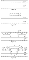
- Figures 1A to 1D show steps in the manufacture of one cell of a vertical DMOS transistor according to the prior art.
- a first step begins with a highly n doped semiconductor layer 10 covered with a lightly doped n type layer 12 on its upper surface.
- Layer 12 is generally an epitaxied layer.
- the highly n doped region 10 may be a substrate or a buried layer within a p type substrate.
- a gate insulator region 14 and a gate electrode 16 are formed on the upper surface of the epitaxied layer 12.
- a p type body region 18 is introduced on both sides of the gate electrode 16. Typically, this region is formed by photolithographic masking followed by a p type implantation and a first thermal anneal step, at a very high temperature and over a long period of time. Subsequent to the thermal anneal step, each body region 18 extends under the gate electrode by a distance d.
- highly n doped source regions 20 and highly p doped body contact regions 22 are introduced into the body regions 18, adjacent to each end of the gate electrode 16.
- these regions 20, 22 are introduced by photolithographic masking followed by ion implantation and a second thermal anneal step. This second anneal step is performed for a shorter time and at a lower temperature than the first anneal step.
- the length L of the body region remaining at the upper surface of the epitaxied layer 12 is the channel length of the DMOS transistor.
- the highly doped layer 10 corresponds to the drain region of the DMOS transistor.
- the process continues in a known manner, with the formation of interconnect layers, and contacts to gate, source, body and drain. Electrical contact to the drain region 10 is made either by a metallisation of the lower surface of drain region 10 when the drain region is a substrate, or at the upper surface of an n type well contacting the drain region 10, when this is a buried layer.
- the formation of the p body region is typically done by implanting boron ions at an energy of 25 to 35keV and an intensity of 2x10 13 to 4x10 13 atoms.cm -2 .
- a severe thermal anneal step is then required to achieve a sufficient distance d of diffusion of this p body implant under the gate electrode.
- a thermal anneal step may typically involve heating the circuit to 1160°C for a period of 1 to 2 hours.
- Use of a dopant with a lower diffusion coefficient would require even more severe diffusion conditions, or may not even be possible.
- a horizontal DMOS structure may be formed where the p body dopant is introduced on only one side of the gate electrode 16. A highly n doped drain contact region is then introduced on the other side of the gate electrode.
- DMOS complementary metal-oxide-semiconductor
- CMOS complementary metal-oxide-semiconductor
- bipolar circuitry is required for treating analogue signals, CMOS transistors for control logic circuitry, and DMOS transistors for a high power interface to control the disc drive motors.
- CMOS transistors are incompatible with known processes for producing CMOS integrated circuits having transistor gate lengths of approximately 1,5 ⁇ m or less.
- a threshold adjust region must be included under the gates of CMOS transistors to achieve a desired threshold voltage. Subjecting such a transistor to a severe anneal step as described above would suppress the threshold adjust region by diffusion effects, and the threshold voltages would no longer be controllable.
- the severe first thermal anneal step described above would weaken the gate insulator layer, and reduce its breakdown voltage to an unacceptable level.
- the severe thermal anneal step cannot simply be eliminated, as the high doping density of the source region 20 compared to the p body region 18, would preclude the choice of a pair of dopants allowing an optimised channel region to be formed.
- An object of the present invention is to provide a method of fabricating DMOS transistors which are suitable for inclusion in manufacturing processes for CMOS integrated circuits with a transistor gate length of 1,5 ⁇ m and less.
- a second object of the present invention is to provide such a process which does not require a high temperature, long duration anneal step.
- a third object of the present invention is to provide such a method which introduces as few new steps as possible into the manufacturing process for CMOS integrated circuits.
- the invention also provides a method of manufacture of a diffused channel insulated gate field effect transistor, as claimed in claim 1.
- FIGS 2A to 2D illustrate a preferred process for the manufacture of DMOS transistors in integrated circuits containing both DMOS and CMOS transistors, according to the present invention.
- Features common with those shown in figures 1A to 1D carry identical reference labels.
- a highly n doped semiconductor layer 10 is provided with a lightly n doped epitaxial layer 12, a gate insulator layer 14 and gate electrode 16 as described with reference to figures 1A and 1B.
- the device shown in figure 2A is created through the performance of a number of manufacturing steps.
- the semiconductor layer 10 is covered with the lightly doped n type layer on its upper surface.
- layer 12 is an epitaxied layer.
- the gate insulator layer 14 and the gate electrode 16 are formed on the upper surface of layer 12.
- P type body implants 24 are formed adjacent to both ends of the gate electrode 16.
- no thermal anneal step is applied. Accordingly, the p type dopant does not diffuse into the semiconductor, neither vertically nor under the gate electrode.
- Figure 2B shows the structure at a later step in the process of the present invention.
- a light n type implant 26 has been formed in the same regions as the p body implants 24. No anneal is performed at this stage, so this implant also does not diffuse into the semiconductor.
- spacers 28 are produced adjacent to each end of the gate electrode. Spacers 28 may correspond to those currently used in the manufacturing of CMOS transistors.
- spacers such as spacers 28 allow the formation of lightly doped drain (LDD) regions between highly doped source and drain regions and the channel region. Without these LDD regions, the peak of the electric field would be at the edge of the drain region, just under the gate electrode 16. Such high electric fields could cause hot carrier injection into the gate insulation layer 14 and gate electrode 16.
- LDD regions displace the point of maximum field strength to a location under the spacers 28, so that no damage to the gate insulation layer 14 can occur.
- Vertical DMOS transistors do not experience the problem of hot carrier injection. The presence of spacers does not appear to bring similar advantages to these structures. Accordingly, the step for forming spacers 28 is not performed in conventional DMOS manufacturing processes.
- the highly n doped source regions 30 are formed, along with highly p doped body contact regions 32.
- the DMOS channel region is formed.
- the DMOS channel region is not defined by the difference between a p type diffusion 18 and a highly doped n type diffusion 20 as in conventional devices. Instead, the DMOS channel region is defined by the difference between a p type diffusion 24 and an intermediately doped n diffusion 26. It is this arrangement which makes possible the realisation of the DMOS channel in a single thermal anneal step.
- the dopant which forms the p body region 24 is boron, implanted at an energy of 40keV, at a dose of 4x10 13 atoms.cm -2 .
- the dopant which forms the lightly doped n regions 26 is preferably arsenic implanted at an energy of 40keV, at a dose of 3x10 13 atoms.cm -2 .
- This light n implant is preferably the same as that used to produce lightly doped drain (LDD) regions in n channel MOS transistors of the integrated circuit.
- the dopant which forms the highly n doped source regions 30 is preferably arsenic, implanted at an energy of 40keV, at a dose of 4x10 15 atoms.cm -2 .
- This n type implant is preferably the same as that used to produce drain and source regions in n channel MOS transistors of the integrated circuit.
- the p body contact regions 32 are also doped with boron. However, to ensure that they have a depth after the thermal anneal step less than that of the p body 24, an implant species such as BF 2 is preferably used, which penetrates less deeply into the semiconductor than boron, and so produces a shallower region after anneal. This same dopant implant may be used to produce source and drain regions for p channel MOS transistors.
- the structure may be heated to 980°C for 30 minutes, which corresponds to normal conditions for CMOS circuit manufacture.
- This allows the production of a 0.25 ⁇ m channel length, and the following diffusion profiles: Cs (atoms.cm -3 ) xj ( ⁇ m) p body 24 2x10 18 0.5 lightly doped n 26 4x10 18 0.15 n source 30 3x10 20 0.25 p body contact 32 1x10 20 0.5 where Cs represents a surface concentration, and xj a corresponding junction depth of a particular region.
- the dimensions of the DMOS transistor should be fixed to withstand a voltage of 20V, both to withstand voltage peaks caused by the inductance of the motor, and to allow for variation of the breakdown voltage with temperature.
- This may be achieved with the vertical DMOS structure of figure 2D, having a 2.5 ⁇ m long gate electrode 16, a 3 ⁇ m thick epitaxial layer 12, with a resistivity of 1 ⁇ .cm.
- Such a structure could have a breakdown voltage as high as 35V. Lower resistivity and greater thickness of the epitaxial layer 12 would give a higher breakdown voltage.
- a DMOS transistor is provided that may be incorporated into a standard CMOS logic or bipolar circuit manufacturing process, with only the addition of a single p body region implant.
Landscapes
- Metal-Oxide And Bipolar Metal-Oxide Semiconductor Integrated Circuits (AREA)
- Insulated Gate Type Field-Effect Transistor (AREA)
Claims (5)
- Verfahren zum Herstellen eines Diffusionskanal-Isolierschicht-Feldeffekt-Transistors mit den folgenden Verfahrensschritten:Bereitstellen eines Halbleitersubstrats (10, 12) mit einer ersten Leitfähigkeitscharakteristik, das eine Oberfläche aufweist;Definieren einer Gate-Isolierschicht (14) und einer Gate-Elektrode (16) an der Oberfläche des Substrats;Einbringen eines ersten Dotierstoffs (24) mit einer zweiten Leitfähigkeitscharakteristik in einen ersten Bereich des Substrats, der einem ersten Ende der Gate-Elektrode benachbart ist, wobei nach diesem Einbringen nicht geglüht wird;Einbringen eines zweiten Dotierstoffs (26) mit einer ersten Leitfähigkeitscharakteristik bei einer geringen Dichte in den ersten Bereich des Substrats;Bilden von Distanzstücken (28), die zumindest dem ersten Ende der Gate-Elektrode benachbart sind;Einbringen eines dritten Source-Dotierstoffs (30) mit einer ersten Leitfähigkeitscharakteristik bei einer hohen Dotierdichte in einen dem Distanzstück (28) benachbarten Teil des ersten Bereichs;Glühen, wobei der erste Dotierstoff dazu ausgelegt wird, während des Glühens schneller als der zweite und dritte Dotierstoff zu diffundieren.
- Verfahren nach Anspruch 1, bei dem das Glühen bei einer Temperatur von weniger als 1.000°C durchgeführt wird.
- Verfahren nach Anspruch 2, dadurch gekennzeichnet, daß das Glühen ungefähr 30 Minuten lang durchgeführt wird.
- Verfahren nach Anspruch 3, gekennzeichnet durch die weiteren Verfahrensschritte:Einbringen eines vierten Dotierstoffs (32) mit einer zweiten Leitfähigkeitscharakteristik in zweite Bereiche des Substrats, wo Body-Kontakte zu bilden sind, und daß dieses Einbringen derart durchgeführt wird, daß nach dem Glühen die Diffusionstiefe des vierten Dotierstoffs geringer als die Diffusionstiefe des ersten Dotierstoffs ist.
- Verfahren nach Anspruch 4, dadurch gekennzeichnet, daß der erste Dotierstoff Bor, der zweite und dritte Dotierstoff Arsen und der vierte Dotierstoff Bor sind, der in Form eines Borfluorids eingebracht wird.
Applications Claiming Priority (2)
| Application Number | Priority Date | Filing Date | Title |
|---|---|---|---|
| FR9515446 | 1995-12-18 | ||
| FR9515446A FR2742583B1 (fr) | 1995-12-18 | 1995-12-18 | Transistor a effet de champ a grille isolee et a canal diffuse |
Publications (2)
| Publication Number | Publication Date |
|---|---|
| EP0780908A1 EP0780908A1 (de) | 1997-06-25 |
| EP0780908B1 true EP0780908B1 (de) | 2002-02-27 |
Family
ID=9485923
Family Applications (1)
| Application Number | Title | Priority Date | Filing Date |
|---|---|---|---|
| EP96410124A Expired - Lifetime EP0780908B1 (de) | 1995-12-18 | 1996-12-17 | Isolierschicht-Feldeffekttransistor mit einem diffundierten Kanal |
Country Status (4)
| Country | Link |
|---|---|
| US (1) | US5801078A (de) |
| EP (1) | EP0780908B1 (de) |
| DE (1) | DE69619487T2 (de) |
| FR (1) | FR2742583B1 (de) |
Cited By (1)
| Publication number | Priority date | Publication date | Assignee | Title |
|---|---|---|---|---|
| CN103035678A (zh) * | 2012-06-08 | 2013-04-10 | 上海华虹Nec电子有限公司 | Rf ldmos器件及制造方法 |
Families Citing this family (8)
| Publication number | Priority date | Publication date | Assignee | Title |
|---|---|---|---|---|
| US6455385B1 (en) * | 1998-01-07 | 2002-09-24 | Advanced Micro Devices, Inc. | Semiconductor fabrication with multiple low dose implant |
| US6774001B2 (en) * | 1998-10-13 | 2004-08-10 | Stmicroelectronics, Inc. | Self-aligned gate and method |
| US6235568B1 (en) * | 1999-01-22 | 2001-05-22 | Intel Corporation | Semiconductor device having deposited silicon regions and a method of fabrication |
| US20090159896A1 (en) * | 2007-12-20 | 2009-06-25 | General Electric Company | Silicon carbide mosfet devices and methods of making |
| DE102008046734A1 (de) * | 2008-09-11 | 2010-03-18 | Osram Gesellschaft mit beschränkter Haftung | Verfahren und Schaltungsanordnung zur Erhöhung der Spannungsfestigkeit von Metalloxidtransistoren bei niedrigen Temperaturen |
| KR101578931B1 (ko) * | 2008-12-05 | 2015-12-21 | 주식회사 동부하이텍 | 반도체 소자 및 반도체 소자의 제조 방법 |
| CN102664161B (zh) * | 2012-05-25 | 2016-11-16 | 杭州士兰集成电路有限公司 | 高压bcd工艺中高压器件的隔离结构及其制造方法 |
| CN113113487A (zh) * | 2020-01-13 | 2021-07-13 | 张清纯 | 半导体器件及其制备方法 |
Family Cites Families (10)
| Publication number | Priority date | Publication date | Assignee | Title |
|---|---|---|---|---|
| DE3016749A1 (de) * | 1980-04-30 | 1981-11-05 | Siemens AG, 1000 Berlin und 8000 München | Kontakt fuer mis-halbleiterbauelement und verfahren zu seiner herstellung |
| GB2150348A (en) * | 1983-11-29 | 1985-06-26 | Philips Electronic Associated | Insulated-gate field-effect transistors and their manufacture |
| JP2700025B2 (ja) * | 1985-12-24 | 1998-01-19 | 富士電機株式会社 | バイポーラたて形mosfet |
| JPS6384164A (ja) * | 1986-09-29 | 1988-04-14 | Nissan Motor Co Ltd | 縦形mosfet |
| JPH0687504B2 (ja) * | 1988-04-05 | 1994-11-02 | 株式会社東芝 | 半導体装置 |
| US5187117A (en) * | 1991-03-04 | 1993-02-16 | Ixys Corporation | Single diffusion process for fabricating semiconductor devices |
| US5182222A (en) * | 1991-06-26 | 1993-01-26 | Texas Instruments Incorporated | Process for manufacturing a DMOS transistor |
| US5178370A (en) * | 1991-08-05 | 1993-01-12 | Motorola Inc. | Conductivity modulated insulated gate semiconductor device |
| EP0658940A1 (de) * | 1993-11-23 | 1995-06-21 | Siemens Aktiengesellschaft | Durch Feldeffekt steuerbares Halbleiterbauelement |
| US5510281A (en) * | 1995-03-20 | 1996-04-23 | General Electric Company | Method of fabricating a self-aligned DMOS transistor device using SiC and spacers |
-
1995
- 1995-12-18 FR FR9515446A patent/FR2742583B1/fr not_active Expired - Fee Related
-
1996
- 1996-12-12 US US08/764,356 patent/US5801078A/en not_active Expired - Lifetime
- 1996-12-17 EP EP96410124A patent/EP0780908B1/de not_active Expired - Lifetime
- 1996-12-17 DE DE69619487T patent/DE69619487T2/de not_active Expired - Fee Related
Cited By (2)
| Publication number | Priority date | Publication date | Assignee | Title |
|---|---|---|---|---|
| CN103035678A (zh) * | 2012-06-08 | 2013-04-10 | 上海华虹Nec电子有限公司 | Rf ldmos器件及制造方法 |
| CN103035678B (zh) * | 2012-06-08 | 2015-04-08 | 上海华虹宏力半导体制造有限公司 | Rf ldmos器件及制造方法 |
Also Published As
| Publication number | Publication date |
|---|---|
| DE69619487T2 (de) | 2002-10-10 |
| FR2742583A1 (fr) | 1997-06-20 |
| US5801078A (en) | 1998-09-01 |
| DE69619487D1 (de) | 2002-04-04 |
| FR2742583B1 (fr) | 1998-04-24 |
| EP0780908A1 (de) | 1997-06-25 |
Similar Documents
| Publication | Publication Date | Title |
|---|---|---|
| US5384279A (en) | Method of manufacturing a semiconductor device comprising a silicon body in which semiconductor regions are formed by ion implantations | |
| US5783469A (en) | Method for making nitrogenated gate structure for improved transistor performance | |
| US7211871B2 (en) | Transistors of semiconductor devices and methods of fabricating the same | |
| US5943595A (en) | Method for manufacturing a semiconductor device having a triple-well structure | |
| KR940005802B1 (ko) | Cmos 반도체장치 및 그 제조방법 | |
| KR100418435B1 (ko) | 전력 집적회로 소자의 제조 방법 | |
| US5536959A (en) | Self-aligned charge screen (SACS) field effect transistors and methods | |
| KR20000069811A (ko) | 임계전압을 승압하는 웰 부스팅 | |
| US6207510B1 (en) | Method for making an integrated circuit including high and low voltage transistors | |
| KR100260044B1 (ko) | 고속/고성능 모스 트랜지스터 및 그 제조방법 | |
| WO1987002825A1 (en) | A method for mos transistor manufacture | |
| US5021851A (en) | NMOS source/drain doping with both P and As | |
| JP2000188391A (ja) | 半導体集積回路装置の製造方法 | |
| EP0780908B1 (de) | Isolierschicht-Feldeffekttransistor mit einem diffundierten Kanal | |
| US4851360A (en) | NMOS source/drain doping with both P and As | |
| KR100368847B1 (ko) | 절연게이트반도체장치및그제조방법 | |
| EP0893821A1 (de) | Verfahren zur Herstellung eines DMOS-Technologie-Transistors mit nur einer thermischen Behandlung für die Bildung von Source und Körpergebieten | |
| EP0832498B1 (de) | Herstellungsverfahren einer integrierten leistungsschaltungsanordnung | |
| KR0128501B1 (ko) | 반도체 장치 및 그 제조방법 | |
| JPH05121436A (ja) | 薄膜トランジスタおよびその製造方法 | |
| US6576521B1 (en) | Method of forming semiconductor device with LDD structure | |
| US6043544A (en) | Semiconductor gate conductor with a substantially uniform doping profile having minimal susceptibility to dopant penetration into the underlying gate dielectric | |
| KR970053087A (ko) | 반도체 소자의 트랜지스터 제조방법 | |
| US6025238A (en) | Semiconductor device having an nitrogen-rich punchthrough region and fabrication thereof | |
| US6054356A (en) | Transistor and process of making a transistor having an improved LDD masking material |
Legal Events
| Date | Code | Title | Description |
|---|---|---|---|
| PUAI | Public reference made under article 153(3) epc to a published international application that has entered the european phase |
Free format text: ORIGINAL CODE: 0009012 |
|
| AK | Designated contracting states |
Kind code of ref document: A1 Designated state(s): DE FR GB IT |
|
| RIN1 | Information on inventor provided before grant (corrected) |
Inventor name: JIMENEZ, JEAN |
|
| 17P | Request for examination filed |
Effective date: 19971210 |
|
| 17Q | First examination report despatched |
Effective date: 19981218 |
|
| RAP3 | Party data changed (applicant data changed or rights of an application transferred) |
Owner name: STMICROELECTRONICS S.A. |
|
| GRAG | Despatch of communication of intention to grant |
Free format text: ORIGINAL CODE: EPIDOS AGRA |
|
| GRAG | Despatch of communication of intention to grant |
Free format text: ORIGINAL CODE: EPIDOS AGRA |
|
| GRAH | Despatch of communication of intention to grant a patent |
Free format text: ORIGINAL CODE: EPIDOS IGRA |
|
| GRAH | Despatch of communication of intention to grant a patent |
Free format text: ORIGINAL CODE: EPIDOS IGRA |
|
| RAP1 | Party data changed (applicant data changed or rights of an application transferred) |
Owner name: STMICROELECTRONICS S.A. |
|
| REG | Reference to a national code |
Ref country code: GB Ref legal event code: IF02 |
|
| GRAA | (expected) grant |
Free format text: ORIGINAL CODE: 0009210 |
|
| AK | Designated contracting states |
Kind code of ref document: B1 Designated state(s): DE FR GB IT |
|
| PG25 | Lapsed in a contracting state [announced via postgrant information from national office to epo] |
Ref country code: IT Free format text: LAPSE BECAUSE OF FAILURE TO SUBMIT A TRANSLATION OF THE DESCRIPTION OR TO PAY THE FEE WITHIN THE PRESCRIBED TIME-LIMIT;WARNING: LAPSES OF ITALIAN PATENTS WITH EFFECTIVE DATE BEFORE 2007 MAY HAVE OCCURRED AT ANY TIME BEFORE 2007. THE CORRECT EFFECTIVE DATE MAY BE DIFFERENT FROM THE ONE RECORDED. Effective date: 20020227 |
|
| REF | Corresponds to: |
Ref document number: 69619487 Country of ref document: DE Date of ref document: 20020404 |
|
| ET | Fr: translation filed | ||
| PLBE | No opposition filed within time limit |
Free format text: ORIGINAL CODE: 0009261 |
|
| STAA | Information on the status of an ep patent application or granted ep patent |
Free format text: STATUS: NO OPPOSITION FILED WITHIN TIME LIMIT |
|
| 26N | No opposition filed |
Effective date: 20021128 |
|
| PGFP | Annual fee paid to national office [announced via postgrant information from national office to epo] |
Ref country code: FR Payment date: 20041208 Year of fee payment: 9 |
|
| PGFP | Annual fee paid to national office [announced via postgrant information from national office to epo] |
Ref country code: DE Payment date: 20041209 Year of fee payment: 9 |
|
| PGFP | Annual fee paid to national office [announced via postgrant information from national office to epo] |
Ref country code: GB Payment date: 20041215 Year of fee payment: 9 |
|
| PG25 | Lapsed in a contracting state [announced via postgrant information from national office to epo] |
Ref country code: GB Free format text: LAPSE BECAUSE OF NON-PAYMENT OF DUE FEES Effective date: 20051217 |
|
| PG25 | Lapsed in a contracting state [announced via postgrant information from national office to epo] |
Ref country code: DE Free format text: LAPSE BECAUSE OF NON-PAYMENT OF DUE FEES Effective date: 20060701 |
|
| GBPC | Gb: european patent ceased through non-payment of renewal fee |
Effective date: 20051217 |
|
| PG25 | Lapsed in a contracting state [announced via postgrant information from national office to epo] |
Ref country code: FR Free format text: LAPSE BECAUSE OF NON-PAYMENT OF DUE FEES Effective date: 20060831 |
|
| REG | Reference to a national code |
Ref country code: FR Ref legal event code: ST Effective date: 20060831 |