EP0780903A2 - Flache Bildaufnahmevorrichtung mit gemeinsamer gemusterter Elektrode - Google Patents
Flache Bildaufnahmevorrichtung mit gemeinsamer gemusterter Elektrode Download PDFInfo
- Publication number
- EP0780903A2 EP0780903A2 EP96309189A EP96309189A EP0780903A2 EP 0780903 A2 EP0780903 A2 EP 0780903A2 EP 96309189 A EP96309189 A EP 96309189A EP 96309189 A EP96309189 A EP 96309189A EP 0780903 A2 EP0780903 A2 EP 0780903A2
- Authority
- EP
- European Patent Office
- Prior art keywords
- common electrode
- pixel
- disposed
- column
- array
- Prior art date
- Legal status (The legal status is an assumption and is not a legal conclusion. Google has not performed a legal analysis and makes no representation as to the accuracy of the status listed.)
- Granted
Links
- 238000003384 imaging method Methods 0.000 title claims abstract description 29
- 238000010168 coupling process Methods 0.000 claims abstract description 25
- 238000005859 coupling reaction Methods 0.000 claims abstract description 25
- 230000008878 coupling Effects 0.000 claims abstract description 17
- 230000005855 radiation Effects 0.000 claims abstract description 13
- 239000000758 substrate Substances 0.000 claims description 5
- XLOMVQKBTHCTTD-UHFFFAOYSA-N Zinc monoxide Chemical compound [Zn]=O XLOMVQKBTHCTTD-UHFFFAOYSA-N 0.000 claims description 4
- 239000004020 conductor Substances 0.000 claims description 4
- AMGQUBHHOARCQH-UHFFFAOYSA-N indium;oxotin Chemical compound [In].[Sn]=O AMGQUBHHOARCQH-UHFFFAOYSA-N 0.000 claims description 4
- 239000010409 thin film Substances 0.000 claims description 4
- 238000000926 separation method Methods 0.000 claims description 3
- XOLBLPGZBRYERU-UHFFFAOYSA-N tin dioxide Chemical compound O=[Sn]=O XOLBLPGZBRYERU-UHFFFAOYSA-N 0.000 claims description 2
- 229910001887 tin oxide Inorganic materials 0.000 claims description 2
- 239000011787 zinc oxide Substances 0.000 claims description 2
- 239000000463 material Substances 0.000 description 6
- 230000001808 coupling effect Effects 0.000 description 4
- 230000004907 flux Effects 0.000 description 4
- 239000007787 solid Substances 0.000 description 4
- 230000008859 change Effects 0.000 description 3
- 239000003989 dielectric material Substances 0.000 description 3
- 238000002594 fluoroscopy Methods 0.000 description 3
- 230000000694 effects Effects 0.000 description 2
- 230000005669 field effect Effects 0.000 description 2
- 238000000034 method Methods 0.000 description 2
- 230000009467 reduction Effects 0.000 description 2
- 239000004642 Polyimide Substances 0.000 description 1
- 229910052581 Si3N4 Inorganic materials 0.000 description 1
- 229910021417 amorphous silicon Inorganic materials 0.000 description 1
- 238000004458 analytical method Methods 0.000 description 1
- 238000003491 array Methods 0.000 description 1
- 239000003990 capacitor Substances 0.000 description 1
- 230000015556 catabolic process Effects 0.000 description 1
- 238000005229 chemical vapour deposition Methods 0.000 description 1
- 238000010276 construction Methods 0.000 description 1
- 238000006731 degradation reaction Methods 0.000 description 1
- 230000001419 dependent effect Effects 0.000 description 1
- 238000001514 detection method Methods 0.000 description 1
- 239000007772 electrode material Substances 0.000 description 1
- 238000005530 etching Methods 0.000 description 1
- 230000008020 evaporation Effects 0.000 description 1
- 238000001704 evaporation Methods 0.000 description 1
- 230000005284 excitation Effects 0.000 description 1
- 230000001939 inductive effect Effects 0.000 description 1
- 230000010354 integration Effects 0.000 description 1
- 230000003993 interaction Effects 0.000 description 1
- 229910052751 metal Inorganic materials 0.000 description 1
- 239000002184 metal Substances 0.000 description 1
- 229920001721 polyimide Polymers 0.000 description 1
- 230000008569 process Effects 0.000 description 1
- 238000001959 radiotherapy Methods 0.000 description 1
- HQVNEWCFYHHQES-UHFFFAOYSA-N silicon nitride Chemical compound N12[Si]34N5[Si]62N3[Si]51N64 HQVNEWCFYHHQES-UHFFFAOYSA-N 0.000 description 1
- 238000001356 surgical procedure Methods 0.000 description 1
Images

Classifications
-
- H—ELECTRICITY
- H10—SEMICONDUCTOR DEVICES; ELECTRIC SOLID-STATE DEVICES NOT OTHERWISE PROVIDED FOR
- H10F—INORGANIC SEMICONDUCTOR DEVICES SENSITIVE TO INFRARED RADIATION, LIGHT, ELECTROMAGNETIC RADIATION OF SHORTER WAVELENGTH OR CORPUSCULAR RADIATION
- H10F39/00—Integrated devices, or assemblies of multiple devices, comprising at least one element covered by group H10F30/00, e.g. radiation detectors comprising photodiode arrays
- H10F39/10—Integrated devices
- H10F39/12—Image sensors
Definitions
- This invention relates generally to solid state radiation imagers and in particular to structures in such imagers to reduce phantom noise and image artifacts.
- Solid state radiation imagers typically comprise a large flat panel imaging device having a plurality of pixels arranged in rows and columns. Each pixel includes a photosensor, such as a photodiode, that is coupled via a switching transistor to two separate address lines, a scan line and a data line. In each row of pixels, each respective switching transistor (typically a thin film field effect transistor (FET)) is coupled to a common scan line through that transistor's gate electrode. In each column of pixels, the readout electrode of the transistor (e.g., the source electrode of the FET) is coupled to a data line, which in tum is selectively coupled to a readout amplifier.
- FET thin film field effect transistor
- radiation such as an x-ray flux
- the x-rays passing through the subject being examined are incident on the imaging array.
- the radiation is incident on a scintillator material and the pixel photosensors measure (by way of change in the charge across the diode) the amount of light generated by x-ray interaction with the scintillator.
- the x-rays can directly generate electron-hole pairs in the photosensor (commonly called "direct detection").
- the photosensor charge data are read out by sequentially enabling rows of pixels (by applying a signal to the scan line causing the switching transistors coupled to that scan line to become conductive), and reading the signal from the respective pixels thus enabled via respective data lines (the photodiode charge signal being coupled to the data line through the conductive switching transistor and associated readout electrode coupled to a data line).
- the photodiode charge signal being coupled to the data line through the conductive switching transistor and associated readout electrode coupled to a data line.
- the performance of flat panel imaging devices is degraded by capacitive coupling between data lines and the pixel photodiode electrodes.
- the x-ray flux remains on during readout of the pixels.
- One example of such operations is fluoroscopy in small or less sophisticated units as might be used in surgery or portable applications; such units use light weight and low cost x-ray generators which must be on continuously to produce an adequate output signal.
- Such units further typically are not adapted to rapidly cycle the x-ray beam on and off during relevant periods to prevent radiating during the readout periods.
- imagers used in conjunction with radiation therapy in which the radiation source is on continuously (to maximize delivered dose) or is pulsed on periodically, which pulses can occur during the readout period.
- This simultaneous excitation of the imager while reading out pixels results in image artifacts or "phantom” images.
- the phantom images occur as a result of capacitive coupling between the respective photodiode electrodes and adjacent data lines; during the readout of a given pixel attached to a given data line.
- the potential of the other pixel electrodes e.g., the non-read pixels
- the change in potential of the pixels not being read out is capacatively coupled into the data line, thereby inducing an additional charge which is read out by the amplifier and presented as part of the signal from the addressed pixel. This effect produces cross-talk or contrast degradation in the image, and is commonly evidenced as bright lines in the display readout.
- a solid state imager array exhibit minimal cross-talk and be capable of generating a stable and accurate image in multiple modes of operation, including modes in which pixels are being read out while the x-ray flux is being applied.
- a flat panel radiation imaging device that exhibits reduced capacitive coupling between pixel photodiode electrodes and readout data lines, and thus exhibits reduced phantom images and image artifacts in operation, includes a low-capacitive-coupling common electrode disposed over a pixel array of photosensors, switching transistors, and address lines that are arranged in an imaging array pattern of rows and columns.
- the low-capacitive coupling common electrode includes a plurality of common electrode column segments oriented along the same axis as the data lines in the array, with each of the common electrode column segments corresponding to a respective column of photosensors in the imaging array pattern.
- Each of the common electrode column segments is disposed so as to have a non-zero setoff distance from data line adjacent to the columns of photosensors and so as to overlie the photosensor pixel electrode by a selected overlap distance, the distance typically being in the range of between 1 and 10 times the vertical separation between the common electrode column segment and the pixel electrode.
- Figure 1(A) is a plan view of a portion of an imager array in accordance with the prior art.
- Figure 1(B) is a partial cross-sectional view of a representative pixel taken along line I-I of Figure 1(A).
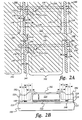
- Figure 2(A) is a partial plan view of a representative portion of the imaging array in accordance with one embodiment of the present invention.
- Figure 2(B) is a cross-sectional view of a representative portion of the imaging array pattern in accordance with the present invention.
- a solid state radiation imager 100 comprises a plurality of pixels 110 (a representative one of which is illustrated in Figure 1(A)) that are arranged in a matrix-like imager array pattern comprising rows and columns of pixels 110.
- imager 100 has a first axis 101 that is the axis along which the rows of pixels are aligned, and a second axis 102 that is the axis along which the columns of pixels are aligned.
- Each pixel 110 comprises a photosensor 120 and a thin film switching transistor 130.
- Photosensor 120 typically comprises a photodiode having a pixel electrode 122 that corresponds with the active (that is, photosensitive) area of the device.
- Switching transistor 130 typically comprises a thin film field effect transistor (FET) having a gate electrode 132, a drain electrode 134 and a source electrode (or readout electrode) 136.
- Imager 100 further comprises a plurality of data lines 140 and scan lines 150 (collectively referred to as address lines). At least one scan line 150 is disposed along first axis 101 for each row of pixels in the imager array pattem. Each scan line is coupled to the respective gate electrodes 132 of pixels in that row of pixels. At least one data line is disposed along second axis 102 for each column of pixels in the imager array pattem, and is coupled to the respective readout electrodes 136 of pixels in that column of pixels.
- FET thin film field effect transistor
- Photodiode 120 is disposed over a substrate 105.
- a first dielectric material layer 121 is typically disposed between pixel electrode 122 and substrate 105.
- Photodiode 120 further comprises a photosensitive material body 124 (typically comprising amorphous silicon) that is electrically coupled to a common electrode 126 that is disposed over the imager array.
- Common electrode 126 comprises an optically transmissive and electrically conductive material, such as indium tin oxide or the like.
- a second dielectric material layer 123 typically comprising silicon nitride or the like, extends over a portion of the sidewalls of the photosensitive material body 124, and a third dielectric layer 125, comprising polyimide or the like, is disposed between common electrode 126 and other components in the imager array (except for the contact point to photosensitive material body 124 through a via in second dielectric material layer 123 and third dielectric layer 125).
- adjacent conductive components refers to components that are spatially near one another but not in direct physical contact so that no direct conductive path (or short circuit) exists between the two components.
- first capacitance C 10 the representation in phantom in Figure 1(B) is for illustrative purposes and does not represent a separate capacitor component in the array
- a second capacitance C 20 denotes capacitive coupling through component above base electrode 122.
- C data line 2 (C 10 + C 20 ) + C 22
- C data line is a function of the induced capacitance to pixels on either side of the data line, hence the factor of two with respect to the sum of C 10 and C 20 .
- Data line capacitance contributes to imager noise in two ways. First, it is an additional load on the amplifier (not shown) that is used to read the charge on a given pixel during the readout sequence in imager operation.
- N Data Line N Data Line
- N Data Line N Data Line
- the capacitive coupling effect is most often of concern in operations in which the imager is excited (that is, the radiation of interest (e.g., x-rays) are incident on the imager) during all or a portion of the time the pixels are being read out.
- the signal read out during the period of time that the imager is excited will be larger than when the imager is not being excited.
- One approximation of this increased normalized to average signal can be expressed as:
- the expression (C10 + C20) represents the coupling capacitance between a single pixel electrode and one adjacent data line; in the array layout, each data line 140 is typically adjacent to two pixel electrodes 140.
- the ratio of the amplifier integration time to line scan time is relatively small, about 0.85 (third term in the equation).
- the second term in the equation has a value of approximately 1 and the size of the coupling effect is 2 [(C 10 + C 20 ) / C pixel ], which ratio provides a useful way to characterize the magnitude of the capacitive coupling effect.
- the value of 2 [(C 10 + C 20 )/C pixel ] calculated from the structure or inferred from imager data is in the range of about 0.5%. This value is significant because typical contrast modulation in x-ray imagers is in the range between about 0.1% and about 10%.
- Radiation imager 100 as described above comprises a low capacitive-coupling patterned common electrode 180 that is disposed over the array photosensors, as illustrated in Figures 2(A) and 2(B).
- Patterned electrode 180 comprises a plurality of common electrode columns 182 that are oriented along second axis 102 of the array such that each respective common electrode column 182 is disposed over a corresponding column of photosensors 120 in the array structure.
- Each common electrode column segment 182 is further disposed such that it does not overlie adjacent data lines 140.
- Adjacent common electrode column segments 182 are electrically coupled to be maintained at a common potential; typically, the respective common electrode column segments 182 are coupled together by at least one common electrode cross-connect segment 184 that is disposed between the column segments; such cross-connect segments can be disposed at every pixel or altematively at multiple-pixel increments along the array, or alternatively only at the edges of the array.
- common electrode column segments may be respectively coupled to a common voltage potential (not shown) off of the array or alternatively to conductive cross-connect shunts off of the array.
- Each common electrode column segment 182 is disposed over a corresponding column of photosensors 120 such that a non-zero overlap distance "D" exists between the edge of common electrode column segment 182 and a pixel second axis boundary edge 128 of photosensor pixel 122 (overlap distance D is determined with respect to boundary edge 128 (oriented along second axis 102) at the portion of pixel electrode 122 underlying the photosensor body (e.g., the semiconductive material of the photodiode) as illustrated in Figure 2(A) and not in the region of TFT 130).
- a non-zero overlap distance "D" exists between the edge of common electrode column segment 182 and a pixel second axis boundary edge 128 of photosensor pixel 122 (overlap distance D is determined with respect to boundary edge 128 (oriented along second axis 102) at the portion of pixel electrode 122 underlying the photosensor body (e.g., the semiconductive material of the photodiode) as illustrated in Figure 2(A) and not in the region of T
- the magnitude of overlap distance "D" between common electrode column segment 182 and pixel boundary 128 is typically in the range between about 1 and 10 times the vertical separation distance "H” between pixel electrode 122 and the portion of common electrode 180 overlying the pixel electrode, and the nominal overlap distance “D” is about 3H.
- "H” typically is in the range of between about 1 ⁇ m and about 2 ⁇ m
- the overlap distance "D” is in the range between about 1 ⁇ m and 20 ⁇ m.
- the lower (or minimum) value of overlap distance "D" is govemed by the concern to have sufficient overlap distance to provide a desired reduction in capacitive coupling between the common electrode and the pixel electrode (while providing sufficient common electrode coverage of photosensor 120 to ensure efficient charge collection at pixel electrode 122 during operation of the imager), and the upper (or maximum) value of overlap distance "D" is governed by the need to maintain a sufficiently high fill factor in the array, that is, the portion of the array area that is occupied by the photosensitive elements of pixels 110. For large area arrays in accordance with this invention, fill factors of about 80% or more are achievable while still maintaining sufficient overlap distance to reduce undesirable capacitive coupling effects.
- Common electrode column segments 182 are further disposed such that each segment has a selected setoff distance "S" between boundary edge 141 of data line electrode 140 disposed adjacent to the column of photosensors 120 underlying the respective common electrode column segment 182 and the boundary (oriented along second axis 102) of the overlying common electrode column segment 182.
- Setoff distance "S” is typically in the range between about 4 ⁇ m and 40 ⁇ m, and nominally about 5 ⁇ m.
- both setoff distance "S" and overlap distance "D” must be considered in combination. For example, if both D and S are large (magnitudes), the array has a poor fill factor; if S is small, data line capacitance increases and the imager exhibits higher noise; if D is small, the imager exhibits increased capacitive coupling.
- cross-connect segment 184 is disposed between adjacent common electrode column segments 182 to electrically couple the respective column segments together.
- Cross connect segment 184 is disposed over a portion of data line 140 that lies between adjacent common electrode column segments 182.
- cross connect segment 184 as illustrated in Figure 2(A) is shown disposed in the lower portion of a pixel 110; alternatively, cross-connect segment 184 is disposed over scan line 150 or over TFT 130.
- the width "W" of cross-connect segment 184 is typically in the range of about 5% to about 40% of the gap distance "G" between the boundaries (along second axis 102) of adjacent common electrode column segments 182.
- Low capacitive-coupling patterned electrode 180 typically comprises a substantially optically transmissive and electrically conductive material such as indium tin oxide, tin oxide, zinc oxide, or the like, that is deposited over the array in a sputter, evaporation, chemical vapor deposition, or similar process and then pattemed using photolithographic etching techniques to provide the desired dimensions of respective common electrode column segments 182 and cross-connect segments 184.
- the thickness of patterned common electrode 180 is typically in the range between about 20 nm and 400 nm for indium tin oxide electrode material.
- Some parts of the common electrode may be opaque conductors such as a metal to shield the FET from light or to increase the electrical conductivity of the common electrode.
- a flat panel radiation imaging device having a low capacitive-coupling patterned common electrode exhibits enhanced performance as the structure provides reduced induced capacitance between data lines and the common electrode, with a consequent reduction of phantom images and image artifacts during imager operation.
- Imager 100 having low capacitive-coupling patterned common electrode 180 in accordance with this invention, exhibits reduced data line capacitance, in comparison with prior art imagers; for example, in an array having a data line having a length of about 10 cm with a pixel pitch of about 200 ⁇ m (that is, the center to center distance between adjacent pixels in a column), it has been calculated that the capacitance of a given data line in an imager in accordance with the present invention is about 22 pf, as compared with a data line capacitance of about 35 pf in a similarly-sized prior art imager.
Landscapes
- Solid State Image Pick-Up Elements (AREA)
- Transforming Light Signals Into Electric Signals (AREA)
- Radiography Using Non-Light Waves (AREA)
- Apparatus For Radiation Diagnosis (AREA)
- Measurement Of Radiation (AREA)
Applications Claiming Priority (2)
| Application Number | Priority Date | Filing Date | Title |
|---|---|---|---|
| US576324 | 1995-12-21 | ||
| US08/576,324 US5648654A (en) | 1995-12-21 | 1995-12-21 | Flat panel imaging device with patterned common electrode |
Publications (3)
| Publication Number | Publication Date |
|---|---|
| EP0780903A2 true EP0780903A2 (de) | 1997-06-25 |
| EP0780903A3 EP0780903A3 (de) | 1998-08-26 |
| EP0780903B1 EP0780903B1 (de) | 2006-08-23 |
Family
ID=24303952
Family Applications (1)
| Application Number | Title | Priority Date | Filing Date |
|---|---|---|---|
| EP96309189A Expired - Lifetime EP0780903B1 (de) | 1995-12-21 | 1996-12-17 | Flache Bildaufnahmevorrichtung mit gemeinsamer gemusterter Elektrode |
Country Status (4)
| Country | Link |
|---|---|
| US (1) | US5648654A (de) |
| EP (1) | EP0780903B1 (de) |
| JP (1) | JP4022276B2 (de) |
| DE (1) | DE69636471T2 (de) |
Cited By (2)
| Publication number | Priority date | Publication date | Assignee | Title |
|---|---|---|---|---|
| EP0838860A2 (de) * | 1996-10-23 | 1998-04-29 | General Electric Company | Strahlungsdetektor mit diskontinuierlichem Dielektrikum |
| EP0964451A3 (de) * | 1998-06-02 | 2000-12-06 | Canon Kabushiki Kaisha | Photosensor und System zur Feststellung von Strahlung |
Families Citing this family (22)
| Publication number | Priority date | Publication date | Assignee | Title |
|---|---|---|---|---|
| KR0183761B1 (ko) * | 1995-11-29 | 1999-03-20 | 김광호 | 고체촬상소자 및 그 제조방법 |
| US5859463A (en) * | 1996-12-23 | 1999-01-12 | General Electric Company | Photosensitive imager contact pad structure |
| US6037609A (en) | 1997-01-17 | 2000-03-14 | General Electric Company | Corrosion resistant imager |
| US6266391B1 (en) * | 1999-08-31 | 2001-07-24 | General Electric Company | Artifact compensation system for matrix-addressed x-ray imaging panel |
| US6404851B1 (en) | 2000-03-30 | 2002-06-11 | General Electric Company | Method and apparatus for automatic exposure control using localized capacitive coupling in a matrix-addressed imaging panel |
| EP1342105A4 (de) * | 2000-11-10 | 2005-09-07 | Hologic Inc | Direkt-röntgenabbildungstafel mit einer abbildungseigenschaft, die umkehrbar mit einer externen energiequelle bei der klinischen benutzung der tafel einstellbar ist |
| US6559506B1 (en) | 2002-04-03 | 2003-05-06 | General Electric Company | Imaging array and methods for fabricating same |
| US6740884B2 (en) * | 2002-04-03 | 2004-05-25 | General Electric Company | Imaging array and methods for fabricating same |
| US6777685B2 (en) * | 2002-04-03 | 2004-08-17 | General Electric Company | Imaging array and methods for fabricating same |
| US6933528B2 (en) * | 2002-04-04 | 2005-08-23 | Nec Lcd Technologies, Ltd. | In-plane switching mode active matrix type liquid crystal display device and method of fabricating the same |
| US6944265B2 (en) * | 2002-11-25 | 2005-09-13 | Ge Medical Systems Global Technology Company, Llc | Image pasting using geometry measurement and a flat-panel detector |
| JP4376522B2 (ja) * | 2003-01-24 | 2009-12-02 | シャープ株式会社 | 電磁波検出器 |
| US6895076B2 (en) * | 2003-06-03 | 2005-05-17 | Ge Medical Systems Global Technology Company, Llc | Methods and apparatus for multiple image acquisition on a digital detector |
| US20040246355A1 (en) * | 2003-06-06 | 2004-12-09 | Ji Ung Lee | Storage capacitor array for a solid state radiation imager |
| US7145152B2 (en) * | 2003-10-14 | 2006-12-05 | General Electric Company | Storage capacitor design for a solid state imager |
| US6982176B2 (en) * | 2003-10-30 | 2006-01-03 | General Electric Company | Method for monitoring production of pixel detectors and detectors produced thereby |
| US7256403B2 (en) | 2004-09-30 | 2007-08-14 | General Electric Company | Photodiode for imaging system and method of making |
| US7207741B2 (en) * | 2004-09-30 | 2007-04-24 | Reliance Electric Technologies, Llc | Bushing system for power transmission products |
| US8430563B2 (en) * | 2009-12-22 | 2013-04-30 | Real Time Imaging Technologies, Llc | Dental fluoroscopic imaging system |
| TWI464715B (zh) * | 2010-06-17 | 2014-12-11 | Au Optronics Corp | 畫素陣列及具有此畫素陣列的顯示面板 |
| JP2013172101A (ja) * | 2012-02-22 | 2013-09-02 | Fujifilm Corp | 放射線検出器、放射線画像撮影装置、及び放射線画像撮影システム |
| EP3244800A1 (de) | 2015-01-12 | 2017-11-22 | Real Time Imaging Technologies, LLC | Niedrigdosiertes röntgenbildgebungssystem |
Family Cites Families (6)
| Publication number | Priority date | Publication date | Assignee | Title |
|---|---|---|---|---|
| US4873516A (en) * | 1987-06-01 | 1989-10-10 | General Electric Company | Method and system for eliminating cross-talk in thin film transistor matrix addressed liquid crystal displays |
| JPH02223927A (ja) * | 1989-02-27 | 1990-09-06 | Hitachi Ltd | 液晶表示パネル |
| US5121214A (en) * | 1990-06-29 | 1992-06-09 | The United States Of America As Represented By The United States Department Of Energy | Method for eliminating artifacts in CCD imagers |
| US5273910A (en) * | 1990-08-08 | 1993-12-28 | Minnesota Mining And Manufacturing Company | Method of making a solid state electromagnetic radiation detector |
| US5187369A (en) * | 1990-10-01 | 1993-02-16 | General Electric Company | High sensitivity, high resolution, solid state x-ray imaging device with barrier layer |
| EP0523784A1 (de) * | 1991-07-15 | 1993-01-20 | Philips Electronics Uk Limited | Bildgebender Detektor und Methode seiner Herstellung |
-
1995
- 1995-12-21 US US08/576,324 patent/US5648654A/en not_active Expired - Lifetime
-
1996
- 1996-12-12 JP JP33133596A patent/JP4022276B2/ja not_active Expired - Fee Related
- 1996-12-17 DE DE69636471T patent/DE69636471T2/de not_active Expired - Fee Related
- 1996-12-17 EP EP96309189A patent/EP0780903B1/de not_active Expired - Lifetime
Non-Patent Citations (1)
| Title |
|---|
| None |
Cited By (3)
| Publication number | Priority date | Publication date | Assignee | Title |
|---|---|---|---|---|
| EP0838860A2 (de) * | 1996-10-23 | 1998-04-29 | General Electric Company | Strahlungsdetektor mit diskontinuierlichem Dielektrikum |
| EP0964451A3 (de) * | 1998-06-02 | 2000-12-06 | Canon Kabushiki Kaisha | Photosensor und System zur Feststellung von Strahlung |
| US6353228B1 (en) | 1998-06-02 | 2002-03-05 | Canon Kabushiki Kaisha | Photosensor, and radiation detection apparatus and system |
Also Published As
| Publication number | Publication date |
|---|---|
| JP4022276B2 (ja) | 2007-12-12 |
| EP0780903A3 (de) | 1998-08-26 |
| US5648654A (en) | 1997-07-15 |
| JPH09247533A (ja) | 1997-09-19 |
| DE69636471D1 (de) | 2006-10-05 |
| EP0780903B1 (de) | 2006-08-23 |
| DE69636471T2 (de) | 2007-03-15 |
Similar Documents
| Publication | Publication Date | Title |
|---|---|---|
| EP0780903B1 (de) | Flache Bildaufnahmevorrichtung mit gemeinsamer gemusterter Elektrode | |
| EP0762506B1 (de) | Flache Bildaufnahmevorrichtung mit planarer Masseelektrode | |
| EP0762507B1 (de) | Festkörperbildaufnahmeanordnung mit Abschirmungsleitern in der Gatelektrodenebene | |
| US5619033A (en) | Layered solid state photodiode sensor array | |
| US5869837A (en) | Radiation imaging panel | |
| JP3469143B2 (ja) | アクティブマトリクス基板及びそれを備えた二次元画像検出器 | |
| US6403965B1 (en) | X-ray image detector system | |
| US6476867B1 (en) | Photoelectric conversion apparatus, driving method and x-ray image pickup apparatus using the same | |
| JP2001509252A (ja) | 電子ノイズの少ない放射線画像形成のためのフラットパネル検出器 | |
| EP1267411A2 (de) | Röntgenbildaufnahmevorrichtung und Ansteuerungsverfahren dafür | |
| EP0686268B1 (de) | Geräuscharme fluoroskopische festkörperbildaufnahmevorrichtung für strahlung | |
| EP1079437B1 (de) | Strahlungsdetektor | |
| US7307301B2 (en) | Imaging array | |
| US5780858A (en) | Electromagnetic radiation imaging device using dual gate thin film transistors | |
| US7112778B2 (en) | Active-matrix substrate and electromagnetic wave detector | |
| KR20010089211A (ko) | 2차원 화상검출기 | |
| EP0523784A1 (de) | Bildgebender Detektor und Methode seiner Herstellung | |
| CN100459135C (zh) | 用于固态辐射成像器的存储电容器阵列 | |
| JP4508429B2 (ja) | センサマトリックス | |
| US7145152B2 (en) | Storage capacitor design for a solid state imager | |
| JPH1152058A (ja) | 2次元放射線検出器 | |
| JP2000111653A (ja) | 放射線2次元検出器 | |
| JP2008244410A (ja) | 画像検出器 |
Legal Events
| Date | Code | Title | Description |
|---|---|---|---|
| PUAI | Public reference made under article 153(3) epc to a published international application that has entered the european phase |
Free format text: ORIGINAL CODE: 0009012 |
|
| AK | Designated contracting states |
Kind code of ref document: A2 Designated state(s): DE FR NL |
|
| PUAL | Search report despatched |
Free format text: ORIGINAL CODE: 0009013 |
|
| AK | Designated contracting states |
Kind code of ref document: A3 Designated state(s): DE FR NL |
|
| 17P | Request for examination filed |
Effective date: 19990226 |
|
| 17Q | First examination report despatched |
Effective date: 20050321 |
|
| GRAP | Despatch of communication of intention to grant a patent |
Free format text: ORIGINAL CODE: EPIDOSNIGR1 |
|
| GRAS | Grant fee paid |
Free format text: ORIGINAL CODE: EPIDOSNIGR3 |
|
| GRAA | (expected) grant |
Free format text: ORIGINAL CODE: 0009210 |
|
| AK | Designated contracting states |
Kind code of ref document: B1 Designated state(s): DE FR NL |
|
| REF | Corresponds to: |
Ref document number: 69636471 Country of ref document: DE Date of ref document: 20061005 Kind code of ref document: P |
|
| ET | Fr: translation filed | ||
| PLBE | No opposition filed within time limit |
Free format text: ORIGINAL CODE: 0009261 |
|
| STAA | Information on the status of an ep patent application or granted ep patent |
Free format text: STATUS: NO OPPOSITION FILED WITHIN TIME LIMIT |
|
| 26N | No opposition filed |
Effective date: 20070524 |
|
| PGFP | Annual fee paid to national office [announced via postgrant information from national office to epo] |
Ref country code: DE Payment date: 20080131 Year of fee payment: 12 |
|
| PG25 | Lapsed in a contracting state [announced via postgrant information from national office to epo] |
Ref country code: DE Free format text: LAPSE BECAUSE OF NON-PAYMENT OF DUE FEES Effective date: 20090701 |
|
| PGFP | Annual fee paid to national office [announced via postgrant information from national office to epo] |
Ref country code: FR Payment date: 20120104 Year of fee payment: 16 |
|
| PGFP | Annual fee paid to national office [announced via postgrant information from national office to epo] |
Ref country code: NL Payment date: 20120103 Year of fee payment: 16 |
|
| REG | Reference to a national code |
Ref country code: NL Ref legal event code: V1 Effective date: 20130701 |
|
| REG | Reference to a national code |
Ref country code: FR Ref legal event code: ST Effective date: 20130830 |
|
| PG25 | Lapsed in a contracting state [announced via postgrant information from national office to epo] |
Ref country code: NL Free format text: LAPSE BECAUSE OF NON-PAYMENT OF DUE FEES Effective date: 20130701 |
|
| PG25 | Lapsed in a contracting state [announced via postgrant information from national office to epo] |
Ref country code: FR Free format text: LAPSE BECAUSE OF NON-PAYMENT OF DUE FEES Effective date: 20130102 |