EP0780490B1 - Appareil de réduction des résidus dans une chambre de traitement de semi-conducteurs - Google Patents
Appareil de réduction des résidus dans une chambre de traitement de semi-conducteurs Download PDFInfo
- Publication number
- EP0780490B1 EP0780490B1 EP96309217A EP96309217A EP0780490B1 EP 0780490 B1 EP0780490 B1 EP 0780490B1 EP 96309217 A EP96309217 A EP 96309217A EP 96309217 A EP96309217 A EP 96309217A EP 0780490 B1 EP0780490 B1 EP 0780490B1
- Authority
- EP
- European Patent Office
- Prior art keywords
- chamber
- ceramic
- pedestal
- processing
- exhaust
- Prior art date
- Legal status (The legal status is an assumption and is not a legal conclusion. Google has not performed a legal analysis and makes no representation as to the accuracy of the status listed.)
- Expired - Lifetime
Links
Images


Classifications
-
- H—ELECTRICITY
- H01—ELECTRIC ELEMENTS
- H01J—ELECTRIC DISCHARGE TUBES OR DISCHARGE LAMPS
- H01J37/00—Discharge tubes with provision for introducing objects or material to be exposed to the discharge, e.g. for the purpose of examination or processing thereof
- H01J37/32—Gas-filled discharge tubes
- H01J37/32431—Constructional details of the reactor
- H01J37/32798—Further details of plasma apparatus not provided for in groups H01J37/3244 - H01J37/32788; special provisions for cleaning or maintenance of the apparatus
- H01J37/32816—Pressure
- H01J37/32834—Exhausting
-
- H—ELECTRICITY
- H01—ELECTRIC ELEMENTS
- H01L—SEMICONDUCTOR DEVICES NOT COVERED BY CLASS H10
- H01L21/00—Processes or apparatus adapted for the manufacture or treatment of semiconductor or solid state devices or of parts thereof
- H01L21/02—Manufacture or treatment of semiconductor devices or of parts thereof
-
- C—CHEMISTRY; METALLURGY
- C23—COATING METALLIC MATERIAL; COATING MATERIAL WITH METALLIC MATERIAL; CHEMICAL SURFACE TREATMENT; DIFFUSION TREATMENT OF METALLIC MATERIAL; COATING BY VACUUM EVAPORATION, BY SPUTTERING, BY ION IMPLANTATION OR BY CHEMICAL VAPOUR DEPOSITION, IN GENERAL; INHIBITING CORROSION OF METALLIC MATERIAL OR INCRUSTATION IN GENERAL
- C23C—COATING METALLIC MATERIAL; COATING MATERIAL WITH METALLIC MATERIAL; SURFACE TREATMENT OF METALLIC MATERIAL BY DIFFUSION INTO THE SURFACE, BY CHEMICAL CONVERSION OR SUBSTITUTION; COATING BY VACUUM EVAPORATION, BY SPUTTERING, BY ION IMPLANTATION OR BY CHEMICAL VAPOUR DEPOSITION, IN GENERAL
- C23C16/00—Chemical coating by decomposition of gaseous compounds, without leaving reaction products of surface material in the coating, i.e. chemical vapour deposition [CVD] processes
- C23C16/44—Chemical coating by decomposition of gaseous compounds, without leaving reaction products of surface material in the coating, i.e. chemical vapour deposition [CVD] processes characterised by the method of coating
- C23C16/4401—Means for minimising impurities, e.g. dust, moisture or residual gas, in the reaction chamber
-
- C—CHEMISTRY; METALLURGY
- C23—COATING METALLIC MATERIAL; COATING MATERIAL WITH METALLIC MATERIAL; CHEMICAL SURFACE TREATMENT; DIFFUSION TREATMENT OF METALLIC MATERIAL; COATING BY VACUUM EVAPORATION, BY SPUTTERING, BY ION IMPLANTATION OR BY CHEMICAL VAPOUR DEPOSITION, IN GENERAL; INHIBITING CORROSION OF METALLIC MATERIAL OR INCRUSTATION IN GENERAL
- C23C—COATING METALLIC MATERIAL; COATING MATERIAL WITH METALLIC MATERIAL; SURFACE TREATMENT OF METALLIC MATERIAL BY DIFFUSION INTO THE SURFACE, BY CHEMICAL CONVERSION OR SUBSTITUTION; COATING BY VACUUM EVAPORATION, BY SPUTTERING, BY ION IMPLANTATION OR BY CHEMICAL VAPOUR DEPOSITION, IN GENERAL
- C23C16/00—Chemical coating by decomposition of gaseous compounds, without leaving reaction products of surface material in the coating, i.e. chemical vapour deposition [CVD] processes
- C23C16/44—Chemical coating by decomposition of gaseous compounds, without leaving reaction products of surface material in the coating, i.e. chemical vapour deposition [CVD] processes characterised by the method of coating
- C23C16/4412—Details relating to the exhausts, e.g. pumps, filters, scrubbers, particle traps
-
- C—CHEMISTRY; METALLURGY
- C23—COATING METALLIC MATERIAL; COATING MATERIAL WITH METALLIC MATERIAL; CHEMICAL SURFACE TREATMENT; DIFFUSION TREATMENT OF METALLIC MATERIAL; COATING BY VACUUM EVAPORATION, BY SPUTTERING, BY ION IMPLANTATION OR BY CHEMICAL VAPOUR DEPOSITION, IN GENERAL; INHIBITING CORROSION OF METALLIC MATERIAL OR INCRUSTATION IN GENERAL
- C23C—COATING METALLIC MATERIAL; COATING MATERIAL WITH METALLIC MATERIAL; SURFACE TREATMENT OF METALLIC MATERIAL BY DIFFUSION INTO THE SURFACE, BY CHEMICAL CONVERSION OR SUBSTITUTION; COATING BY VACUUM EVAPORATION, BY SPUTTERING, BY ION IMPLANTATION OR BY CHEMICAL VAPOUR DEPOSITION, IN GENERAL
- C23C16/00—Chemical coating by decomposition of gaseous compounds, without leaving reaction products of surface material in the coating, i.e. chemical vapour deposition [CVD] processes
- C23C16/44—Chemical coating by decomposition of gaseous compounds, without leaving reaction products of surface material in the coating, i.e. chemical vapour deposition [CVD] processes characterised by the method of coating
- C23C16/455—Chemical coating by decomposition of gaseous compounds, without leaving reaction products of surface material in the coating, i.e. chemical vapour deposition [CVD] processes characterised by the method of coating characterised by the method used for introducing gases into reaction chamber or for modifying gas flows in reaction chamber
- C23C16/45502—Flow conditions in reaction chamber
-
- C—CHEMISTRY; METALLURGY
- C23—COATING METALLIC MATERIAL; COATING MATERIAL WITH METALLIC MATERIAL; CHEMICAL SURFACE TREATMENT; DIFFUSION TREATMENT OF METALLIC MATERIAL; COATING BY VACUUM EVAPORATION, BY SPUTTERING, BY ION IMPLANTATION OR BY CHEMICAL VAPOUR DEPOSITION, IN GENERAL; INHIBITING CORROSION OF METALLIC MATERIAL OR INCRUSTATION IN GENERAL
- C23C—COATING METALLIC MATERIAL; COATING MATERIAL WITH METALLIC MATERIAL; SURFACE TREATMENT OF METALLIC MATERIAL BY DIFFUSION INTO THE SURFACE, BY CHEMICAL CONVERSION OR SUBSTITUTION; COATING BY VACUUM EVAPORATION, BY SPUTTERING, BY ION IMPLANTATION OR BY CHEMICAL VAPOUR DEPOSITION, IN GENERAL
- C23C16/00—Chemical coating by decomposition of gaseous compounds, without leaving reaction products of surface material in the coating, i.e. chemical vapour deposition [CVD] processes
- C23C16/44—Chemical coating by decomposition of gaseous compounds, without leaving reaction products of surface material in the coating, i.e. chemical vapour deposition [CVD] processes characterised by the method of coating
- C23C16/458—Chemical coating by decomposition of gaseous compounds, without leaving reaction products of surface material in the coating, i.e. chemical vapour deposition [CVD] processes characterised by the method of coating characterised by the method used for supporting substrates in the reaction chamber
- C23C16/4582—Rigid and flat substrates, e.g. plates or discs
- C23C16/4583—Rigid and flat substrates, e.g. plates or discs the substrate being supported substantially horizontally
- C23C16/4586—Elements in the interior of the support, e.g. electrodes, heating or cooling devices
-
- C—CHEMISTRY; METALLURGY
- C23—COATING METALLIC MATERIAL; COATING MATERIAL WITH METALLIC MATERIAL; CHEMICAL SURFACE TREATMENT; DIFFUSION TREATMENT OF METALLIC MATERIAL; COATING BY VACUUM EVAPORATION, BY SPUTTERING, BY ION IMPLANTATION OR BY CHEMICAL VAPOUR DEPOSITION, IN GENERAL; INHIBITING CORROSION OF METALLIC MATERIAL OR INCRUSTATION IN GENERAL
- C23C—COATING METALLIC MATERIAL; COATING MATERIAL WITH METALLIC MATERIAL; SURFACE TREATMENT OF METALLIC MATERIAL BY DIFFUSION INTO THE SURFACE, BY CHEMICAL CONVERSION OR SUBSTITUTION; COATING BY VACUUM EVAPORATION, BY SPUTTERING, BY ION IMPLANTATION OR BY CHEMICAL VAPOUR DEPOSITION, IN GENERAL
- C23C16/00—Chemical coating by decomposition of gaseous compounds, without leaving reaction products of surface material in the coating, i.e. chemical vapour deposition [CVD] processes
- C23C16/44—Chemical coating by decomposition of gaseous compounds, without leaving reaction products of surface material in the coating, i.e. chemical vapour deposition [CVD] processes characterised by the method of coating
- C23C16/46—Chemical coating by decomposition of gaseous compounds, without leaving reaction products of surface material in the coating, i.e. chemical vapour deposition [CVD] processes characterised by the method of coating characterised by the method used for heating the substrate
- C23C16/463—Cooling of the substrate
-
- C—CHEMISTRY; METALLURGY
- C30—CRYSTAL GROWTH
- C30B—SINGLE-CRYSTAL GROWTH; UNIDIRECTIONAL SOLIDIFICATION OF EUTECTIC MATERIAL OR UNIDIRECTIONAL DEMIXING OF EUTECTOID MATERIAL; REFINING BY ZONE-MELTING OF MATERIAL; PRODUCTION OF A HOMOGENEOUS POLYCRYSTALLINE MATERIAL WITH DEFINED STRUCTURE; SINGLE CRYSTALS OR HOMOGENEOUS POLYCRYSTALLINE MATERIAL WITH DEFINED STRUCTURE; AFTER-TREATMENT OF SINGLE CRYSTALS OR A HOMOGENEOUS POLYCRYSTALLINE MATERIAL WITH DEFINED STRUCTURE; APPARATUS THEREFOR
- C30B25/00—Single-crystal growth by chemical reaction of reactive gases, e.g. chemical vapour-deposition growth
- C30B25/02—Epitaxial-layer growth
-
- H—ELECTRICITY
- H01—ELECTRIC ELEMENTS
- H01J—ELECTRIC DISCHARGE TUBES OR DISCHARGE LAMPS
- H01J37/00—Discharge tubes with provision for introducing objects or material to be exposed to the discharge, e.g. for the purpose of examination or processing thereof
- H01J37/32—Gas-filled discharge tubes
- H01J37/32431—Constructional details of the reactor
- H01J37/32458—Vessel
- H01J37/32477—Vessel characterised by the means for protecting vessels or internal parts, e.g. coatings
-
- H—ELECTRICITY
- H01—ELECTRIC ELEMENTS
- H01J—ELECTRIC DISCHARGE TUBES OR DISCHARGE LAMPS
- H01J37/00—Discharge tubes with provision for introducing objects or material to be exposed to the discharge, e.g. for the purpose of examination or processing thereof
- H01J37/32—Gas-filled discharge tubes
- H01J37/32431—Constructional details of the reactor
- H01J37/32715—Workpiece holder
- H01J37/32724—Temperature
-
- H—ELECTRICITY
- H01—ELECTRIC ELEMENTS
- H01L—SEMICONDUCTOR DEVICES NOT COVERED BY CLASS H10
- H01L21/00—Processes or apparatus adapted for the manufacture or treatment of semiconductor or solid state devices or of parts thereof
- H01L21/67—Apparatus specially adapted for handling semiconductor or electric solid state devices during manufacture or treatment thereof; Apparatus specially adapted for handling wafers during manufacture or treatment of semiconductor or electric solid state devices or components ; Apparatus not specifically provided for elsewhere
- H01L21/683—Apparatus specially adapted for handling semiconductor or electric solid state devices during manufacture or treatment thereof; Apparatus specially adapted for handling wafers during manufacture or treatment of semiconductor or electric solid state devices or components ; Apparatus not specifically provided for elsewhere for supporting or gripping
- H01L21/687—Apparatus specially adapted for handling semiconductor or electric solid state devices during manufacture or treatment thereof; Apparatus specially adapted for handling wafers during manufacture or treatment of semiconductor or electric solid state devices or components ; Apparatus not specifically provided for elsewhere for supporting or gripping using mechanical means, e.g. chucks, clamps or pinches
- H01L21/68714—Apparatus specially adapted for handling semiconductor or electric solid state devices during manufacture or treatment thereof; Apparatus specially adapted for handling wafers during manufacture or treatment of semiconductor or electric solid state devices or components ; Apparatus not specifically provided for elsewhere for supporting or gripping using mechanical means, e.g. chucks, clamps or pinches the wafers being placed on a susceptor, stage or support
- H01L21/68742—Apparatus specially adapted for handling semiconductor or electric solid state devices during manufacture or treatment thereof; Apparatus specially adapted for handling wafers during manufacture or treatment of semiconductor or electric solid state devices or components ; Apparatus not specifically provided for elsewhere for supporting or gripping using mechanical means, e.g. chucks, clamps or pinches the wafers being placed on a susceptor, stage or support characterised by a lifting arrangement, e.g. lift pins
-
- H—ELECTRICITY
- H01—ELECTRIC ELEMENTS
- H01L—SEMICONDUCTOR DEVICES NOT COVERED BY CLASS H10
- H01L21/00—Processes or apparatus adapted for the manufacture or treatment of semiconductor or solid state devices or of parts thereof
- H01L21/67—Apparatus specially adapted for handling semiconductor or electric solid state devices during manufacture or treatment thereof; Apparatus specially adapted for handling wafers during manufacture or treatment of semiconductor or electric solid state devices or components ; Apparatus not specifically provided for elsewhere
- H01L21/683—Apparatus specially adapted for handling semiconductor or electric solid state devices during manufacture or treatment thereof; Apparatus specially adapted for handling wafers during manufacture or treatment of semiconductor or electric solid state devices or components ; Apparatus not specifically provided for elsewhere for supporting or gripping
- H01L21/687—Apparatus specially adapted for handling semiconductor or electric solid state devices during manufacture or treatment thereof; Apparatus specially adapted for handling wafers during manufacture or treatment of semiconductor or electric solid state devices or components ; Apparatus not specifically provided for elsewhere for supporting or gripping using mechanical means, e.g. chucks, clamps or pinches
- H01L21/68714—Apparatus specially adapted for handling semiconductor or electric solid state devices during manufacture or treatment thereof; Apparatus specially adapted for handling wafers during manufacture or treatment of semiconductor or electric solid state devices or components ; Apparatus not specifically provided for elsewhere for supporting or gripping using mechanical means, e.g. chucks, clamps or pinches the wafers being placed on a susceptor, stage or support
- H01L21/68785—Apparatus specially adapted for handling semiconductor or electric solid state devices during manufacture or treatment thereof; Apparatus specially adapted for handling wafers during manufacture or treatment of semiconductor or electric solid state devices or components ; Apparatus not specifically provided for elsewhere for supporting or gripping using mechanical means, e.g. chucks, clamps or pinches the wafers being placed on a susceptor, stage or support characterised by the mechanical construction of the susceptor, stage or support
-
- H—ELECTRICITY
- H01—ELECTRIC ELEMENTS
- H01J—ELECTRIC DISCHARGE TUBES OR DISCHARGE LAMPS
- H01J2237/00—Discharge tubes exposing object to beam, e.g. for analysis treatment, etching, imaging
- H01J2237/02—Details
- H01J2237/022—Avoiding or removing foreign or contaminating particles, debris or deposits on sample or tube
-
- Y—GENERAL TAGGING OF NEW TECHNOLOGICAL DEVELOPMENTS; GENERAL TAGGING OF CROSS-SECTIONAL TECHNOLOGIES SPANNING OVER SEVERAL SECTIONS OF THE IPC; TECHNICAL SUBJECTS COVERED BY FORMER USPC CROSS-REFERENCE ART COLLECTIONS [XRACs] AND DIGESTS
- Y10—TECHNICAL SUBJECTS COVERED BY FORMER USPC
- Y10S—TECHNICAL SUBJECTS COVERED BY FORMER USPC CROSS-REFERENCE ART COLLECTIONS [XRACs] AND DIGESTS
- Y10S156/00—Adhesive bonding and miscellaneous chemical manufacture
- Y10S156/916—Differential etching apparatus including chamber cleaning means or shield for preventing deposits
Definitions
- the present invention relates to an apparatus for reducing residues inside a semiconductor processing chamber.
- deposition gas molecules are deposited on the surface of a substrate. Some of these molecules also come in contact with areas of the chamber, such as the aluminum walls, resulting in the unwanted deposition of material and residues.
- areas of the chamber such as the aluminum walls
- flakes or particles of the deposited material can break off from the surface of the chamber onto the substrate being processed, potentially causing a defect.
- Surface deposits also adversely effect other processing conditions such as deposition uniformity, deposition rate, film strength and the like.
- processing chambers are periodically cleaned to remove the material deposited by the deposition gases.
- Various techniques have been used or proposed for cleaning residues from interior surfaces of a processing chamber.
- One conventional cleaning technique involves physically cleaning the interior surfaces of the processing chamber by way of rinse water and clean wipes.
- a limitation with this technique is that the processing apparatus often operates no more than 1000 to 2000 runs before substantial residues build up on its interior surfaces. To remove these deposits with a rinse water and clean wipe requires that the processing apparatus be taken down to clean its interior surfaces.
- this conventional cleaning process often takes several hours or more to perform. Taking a machine down for hours at a time clearly impacts wafer throughput in the fabrication plant.
- etching gases such as fluorine
- the plasma enhanced etching gases can be used periodically after a group of N wafers has been processed or after every wafer.
- the etching gases react with the deposited material so as to remove it from the surfaces of the processing chamber.
- Such techniques often cannot remove all the aluminum and organic residues from the chamber walls without other detrimental effects.
- the etchant gases can increase the amount of particles into the processing chamber from precipitates derived from the etching gases and the like.
- precipitates examples include aluminum oxide, aluminum fluoride, aluminum oxy-fluoride, and others.
- the precipitates increase the particle count in the processing chamber, which is clearly an undesirable result.
- the use of such etchant gases in a clean step requires additional processing time thereby decreasing wafer throughput.
- the physical cleaning techniques described above are often used in conjunction with etching gases to periodically clean the residues and precipitates which remain after a chamber clean. However, as described above, the physical clean process results in further down time of the processing machine and lower wafer throughput.
- the chamber is cylindrical in shape.
- the chamber includes a heated pedestal 10 for supporting a substrate or wafer 12 for processing and a shower head 14 for dispersing process gases above the wafer under plasma conditions.
- the plasma is formed between shower head 14 and substrate 12 by using an RF source 16 to apply a potential to the shower head, with the pedestal 10 being grounded.
- chamber walls 18 are also grounded.
- the chamber walls are insulated from the voltage applied to the shower head by RF insulators 20. Since this is a cross section, RF insulator 20 is a ring around the circular shower head 14.
- the process gases are applied through shower head 14 to wafer 12.
- An exhaust channel 22 is formed in the chamber wall, as an annular ring. At one point, there is a port 24 connected to a vacuum pump to draw out the exhaust gases.
- a plasma enhanced CVD film of silicon nitride is deposited on wafer 12 using a recipe requiring silane, N 2 O and ammonia or a similar recipe.
- the deposited nitride film forms on the surface of wafer 12.
- films can also deposit on the chamber itself, forming an undesirable residue which could contaminate subsequent process steps.
- the primary area of deposits are on the chamber walls adjacent the exhaust channel 22. Because gas is being forced through the gas distribution manifold, less of the reactant will form on the gas distribution manifold itself, since it is directed away by the incoming gas. In addition, the gas distribution manifold is hotter than other parts of the chamber, since it is in contact with generated plasma, and the heat reduces residue build-up.
- a purge gas is forced up along the sides of pedestal 10 between it and the chamber walls 18 along a path 26.
- the purpose of the purge gas is to avoid deposits at undesirable locations and prevent deposits on the wafer edges. Accordingly, this is one method of protecting the lower parts of the chamber wall from undesirable residue buildup. Since the vacuum pump draws the exhaust gases, this is a primary area where residue will build up on the chamber walls.
- RF insulator 20 is not connected to ground, and thus less of the plasma forms between it and the shower head, reducing the amount of residue buildup.
- an in-situ plasma clean is typically used to clean these deposits.
- the in-situ clean contains a fluorine species such as CF 4 and an oxide such as O 2 which are ignited under plasma conditions.
- the clean typically removes material deposited during the nitride deposition step, but leaves its own residue as described above.
- the etched away material is pumped by a pumping system, not shown, through exhaust port 24.
- the residue left over from the chamber clean is made up of particles from some or all of a combination of oxygen, nitrogen, silicon, fluorine and similar elements.
- Heaters 28 heat walls 18 of the processing chamber during the clean step to above 100 degrees C. Such an elevated temperature deters deposition of the process and exhaust gases that may otherwise form on the chamber walls.
- the inclusion of heaters 28 adds to the complexity and cost of the processing chamber and requires energy during operation which further increases processing costs. Without heater, the aluminium chamber walls are typically around 70-80°C due to water cooling during processing .
- the US-A-5,304,279 discloses a dry processing apparatus for plasma etching our deposition including a chamber for plasma processing.
- the chamber is lined with a material inert to a plasma and a cover made of quartz.
- the apparatus further comprises a flat insulating ring between the waver and a pedestal therefore.
- the EP-A-0 463 633 discloses a chemical vapour deposition apparatus for reducing particle contamination in a CVD-process, said apparatus comprises a removable baffle having the shape of a truncated cone and being placed in the exhaust line at its junctor to the reaction chamber to prevent contamination particles from re-entering the reaction chamber.
- U.S. Patent No. 5,366,585 discloses the use of a free standing ceramic liner around portions of the chamber wall exposed to the processing plasma.
- the ceramic was found to act as an insulator, reducing the build-up of residue on the electrically conductive aluminium chamber walls. It was disclosed that the ceramic barrier material need not shield the entire inner surface of the process reactor chamber, but it should protect reactor chamber surfaces surrounding the area in which plasma will be generated.
- the liner was preferably 130 micrometers to 6.4 millimeter thick, and made of a non-porous, homogeneous material, such as ceramic alumina.
- the present invention has as its objected to provide an apparatus for applying a processing material to a substrate in which apparatus the residues which are build-up in the processing chamber and the exhaust manifold during processing of the substrate in the processing chamber may be further reduced.
- the apparatus according to the invention is structured as claimed in claim 1.
- the invention provides an apparatus for limiting a residue build-up by lining with a ceramic material the exhaust passage and/or the exhaust plenum of a processing chamber. These exhaust areas attract residue formation due to the funnelling of exhaust gases and particles through this area. Although not in a direct line with the plasma between the gas dispersing manifold and the susceptor, it has been discovered by the inventors that residue build up in the exhaust areas is reduced by a ceramic liner, which need not be as thick as a ceramic liner directly exposed to such plasma.
- the inventors have used an air gap between the ceramic liner and the processing chamber walls to increase the dielectric value of the ceramic liner, and further inhibits the build-up of residues.
- the ceramic liner has been found to retain sufficient heat to allow the elimination of heaters typically used to heat the aluminium walls during a clean operation, if the clean operation is commenced immediately after a process step so that the ceramic retains the necessary heat from the previous processing step. This both saves the time and the power required to heat the chamber and eliminates the need for the heaters.
- the provision of an air gap aids in this heating, preventing the heat from being drawn off by direct contact with the aluminium walls.
- the ceramic liners are attached to the chamber walls with TEFLON ® (polytetrafluoroethylene) screws.
- TEFLON ® polytetrafluoroethylene
- the non-metal TEFLON ® screws avoid a plasma being generated between the screw and the gas discharge manifold, or shower head.
- the surface of the TEFLON ® is less susceptible to particulate formation.
- a ceramic, a ceramic cover is also placed over the pedestal supporting the wafer in order to provide a more uniform plasma flow and to protect the pedestal from residue formation.
- the dielectric value of the ceramic covering on the chamber walls is chosen to be higher than the pedestal ceramic cover in order to ensure that the plasma is primarily directed to the pedestal.
- the different dielectric values are due to differences in material and/or thickness.
- Fig. 2 shows the prior art process chamber of Fig. 1 modified in accordance with the present invention.
- Ceramic rings 30 and 32 have been added to the interior of the process chamber in the exhaust manifold.
- an RF insulator 20' of different shape has been added, extending below gas distribution manifold 14 to provide a narrower gap for the exhaust gases.
- a ceramic pedestal cover 34 is shown. The details of the ceramic pedestal cover and the extended RF insulator 20' are set forth in copending Application Serial NoP8/348273 filed November 30, 1994, entitled “CVD Processing Chamber", assigned to Applied Materials, Inc..
- ceramic pedestal cover 34 also provides the function of adding a dielectric in between the pedestal and the gas distribution manifold to provide a more uniform plasma.
- the narrow gap between the RF insulator 20' and ceramic ring 30 serves to provide pressure differential for an even exhaustion of exhaust gases and thus a more even deposition of the desired material on the wafer substrate 12.
- Fig. 3 is a horizontal cross sectional view illustrating the gas flow in the embodiment of Fig. 2.
- the view looks down on wafer 12 and the annular plenum 222.
- gases are dispersed radially as indicated by arrows 223, passing through the narrow slot between RF insulator ring 20' and ceramic ring 30. These gases then enter plenum 222, and travel in a direction indicated by arrows 235 to the downward extending gas exhaust passage 239.
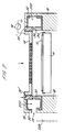
- FIG. 4 An overall, more detailed cross-sectional view of an embodiment of a processing chamber 100 according to the present invention is shown in Fig. 4.
- a heated pedestal 136 centered within processing chamber 100 supports a semiconductor wafer or substrate (not shown) at a wafer processing location 141 on a flat (or slightly convex), circular face 145 of the pedestal.
- a lift mechanism (not shown) raises and lowers heated pedestal 136 and its wafer lift pins 162 as wafers are transferred into and out of the body of the chamber by a robot blade (not shown) through an insertion/removal opening 142 in the side of the chamber.
- the pedestal face 145 is parallel and spaced closely to a process gas distribution faceplate 122 through which process gases enter the chamber.
- An RF power supply (not shown) applies electrical power between the gas distribution faceplate 122 and the pedestal so as to excite the process gas mixture to form a plasma within the cylindrical region between the faceplate and the pedestal.
- the constituents of the plasma react to deposit a desired film on the surface of the semiconductor wafer supported on the face 145 of the pedestal.
- the remainder of the gas mixture, including reaction products, is evacuated from the chamber by a vacuum pump (not shown).
- the aluminum pedestal 136 and the inner surface 265 of the cylindrical side wall of the chamber are lined with a ceramic material (rings 236, 234) to avoid residue build-up.
- the ceramic material also resists corrosion and adjusts the degree of impedance encountered by the plasma as the RF circuit (not shown) seeks to complete its circuit to ground potential.
- the improved uniformity of gas distribution across the wafer and the circular configuration of the chamber 100 and its symmetrical liners (236, 234) help to make the plasma in the chamber more uniform and stable to contribute to an improvement in the uniformity of the thickness of material deposited on the wafer being processed.
- Patent No. 5,366,585 provides further information on the types of ceramics and their thickness and one embodiment of where they are placed.
- the semiconductor wafer (not shown) is supported on the face 145 of the pedestal 136.
- the face 145 is parallel and spaced closely to a process gas distribution faceplate 122 having holes 121 through which process gases enter the chamber. More specifically, deposition process gases flow into the chamber through an inlet manifold 126 (indicated by arrow 123), through a conventional perforated blocker plate 124, and through the holes 121 in a conventional flat, circular gas distribution faceplate 122 (indicated by small arrows 144).
- the elements from inlet manifold 126 to gas distribution faceplate 122 are part of a gas distributor manifold which is a part of the lid to the chamber.
- An RF power supply applies electrical power between the gas distribution faceplate 121 and the pedestal so as to excite the process gas mixture to form a plasma within the cylindrical region between the faceplate and the pedestal. (This region will be referred to herein as the "reaction region”.)
- the constituents of the plasma react to deposit a desired film on the surface of the semiconductor wafer supported on the face 145 of the pedestal.
- the remainder of the gas mixture, including reaction products, is evacuated from the chamber by a vacuum pump (not shown).
- the gases are exhausted through an annular, slot-shaped orifice 131 surrounding the reaction region and into an annular exhaust plenum 222.
- the annular slot 131 and the plenum 222 are defined by the gap between the top of the chamber's cylindrical side wall 134 (including the upper dielectric lining 234 on the wall) and the bottom of the ceramic liner 32 under circular chamber lid 221 (including the dielectric insulator (isolator) 120 between the lid 221 and the perimeter flange 125 of the gas distribution plate 121).
- the 360° circular symmetry and uniformity of the slot orifice 131 and the plenum 222 are important to achieving a uniform flow of process gases over the wafer so as to deposit a uniform film on the wafer.
- the gases flow underneath a viewing port 232, through a downward-extending gas passage 239, past a vacuum shut-off valve 240 (whose body is integrated with the lower chamber body 134), and into the exhaust outlet 226 which connects to the external vacuum pump (not shown).
- the pedestal diameter is 10.3 inches (261.6 mm)
- the inner diameter of the slot orifice 131 is 10.5 inches (267 mm).
- the diameter of a typical wafer support pedestal 136 with ceramic coating is 10.3 in. (261.6 mm).
- the inside and outside diameter of a typical chamber liner e.g., 234, 236) are approximately 10.5 in (266.7 mm) and 12.5 in (317.5 mm), respectively.
- the length of the narrowest passage of the radial slot being approximately 0.5 in (12.7 mm) whose length can be adjusted by changing the relative diameters of the pieces and their overlap.
- the slot gap 131 can similarly be changed.
- a beveled surface can be provided on the bottom surface of the isolator 120 as shown in Fig. 5.
- the above described gap (slot) configuration 131 is useful for example when the chamber internal pressure is maintained at 600 pa (4,5 torr) and a gas flow of 285 sccm SiH 4 , 140 sccm NH 3 and 4000 sccm N 2 is provided to a processing chamber operating at a temperature of approximately 400°C.
- the wafer support pedestal or platen 136 is covered by a corrosion-resistant shield to protect the pedestal from corrosion by process gases, particularly during the plasma etch process used for cleaning the chamber between deposition processes. During both etching and deposition the plasma is excited by applying an RF voltage between the wafer support pedestal and the gas distribution plate 122.
- the shield 34 (see Fig. 2) generally is a dielectric, so it increases the electrical impedance between the plasma and the pedestal.
- the cover plate or shield is a ceramic (preferably aluminum nitride) disc.
- the aluminum chamber side wall 134 would present a lower impedance path for current from the plasma, and therefore would undesirably deflect away from the semiconductor wafer the plasma containing the deposition process reagents, thereby lowering the rate of deposition on the wafer and undesirably depositing material on the chamber walls.
- This problem can be overcome by covering the interior surface of the cylindrical chamber wall with a dielectric lining which imposes an electrical impedance between the chamber wall and the plasma body which is substantially greater than the electrical impedance between the pedestal and the plasma body.
- a high electrical impedance can be achieved by making the dielectric liner on the wall much thicker than the shield disc on the pedestal, and, optionally, by also choosing for the wall liner a material having a lower dielectric constant than the material of the shield disc.
- the inside of the chamber wall is covered by upper and lower annular dielectric liners 234 and 236 (although a single liner could be used).
- the upper liner rests on the lower liner, which rests on a shelf 251 on the chamber wall.
- the inside surface of the chamber lid 221 is covered by the insulator 132 which was described above in regard to its function of insulating the gas distribution plate 122 from the chamber lid.
- the upper and lower wall liners 234 and 236 each are composed of alumina about one inch (25 mm) thick, and the lid insulator 120 is about one inch thick.
- the pedestal shield disc 34 is only about 0.040 inch (1 mm) thick.
- the shield disc is of very uniform thickness, and the pedestal top face is very smooth unanodized aluminum, so as to provide the lowest possible, and most spatially uniform, impedance between the pedestal and the wafer supported thereon. Therefore, the impedance between the pedestal and the plasma body is much less than the impedance between the chamber wall and the plasma body. This promotes efficiency and uniformity of deposition on the semiconductor wafer. (To minimize non-uniformity between the edge and center of the wafer, the gas distribution plate also is larger than the wafer diameter, preferably by about 20%).
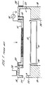
- Fig. 5 is a cross sectional diagram of a portion of the edge of the process chamber showing the exhaust plenum and exhaust port.
- the annular ceramic rings 236 and 234 are shown in more detail, with the plenum 222 formed partially in ring 234.
- ring 234 is attached to the lid assembly via a TEFLON® (polytetrafluoroethylene) screw 40.
- Ring 234 preferably only contacts chamber wall 134 at a few points to limit heat loss.
- Ring 236 simply sits on a shelf 251 of the process wall, and is aligned against a ring 42.
- An air gap between ring 236 and process wall 134 increases the dielectric value and is thus beneficial.
- An air gap between 1 and 25 millimeters is used, preferably a 10 millimeter gap is used.
- An exhaust port viewing window 230 preferably made of single crystal sapphire, allows viewing of any residue building.
- insulator 120 includes a beveled portion 50 which extends down below the level of face plate 122 in order to form a narrow gap between it and ceramic ring 234 for the passage of exhaust gases.
- a series of O-rings provide good contact between various elements, including O-rings in slots 52, 54, and 56 on the lid assembly, and an O-ring slot 58 for the exhaust port assembly.
- Fig. 6 is a diagram of wafer runs showing particulate build-up after different numbers of wafer runs. As can be seen, the number of particles remains relatively constant, and the particle size is small.
- the invention enabled a run of 3600 wafers before doing a cleaning operation. The need for a clean is primarily determined by visual observation of residue build-up through viewing window 232.
- the processing steps for doing a clean according to the present invention are different from a typical processing step.
- a fluorine cleaning operation is typically done after 3600 wafers, rather than 1000-2000 wafers in the prior art process.
- the cleaning step can be initiated immediately upon removal of the wafer in the last processing step, relying on the ceramic liners having retained sufficient heat.
- the ceramic liner is at least 100°C, preferably between 120°C and 170°C.
- this period of time between the end of the process step and the start of a clean operation is no more than a few seconds.
- the cleaning operation can proceed as set forth, for example, in the patents referenced in the background of this application.
- the present invention can be embodied in other specific forms.
- the rings could be of different shapes and could cover the chamber walls without producing the narrow slit for exhaust gas as in the preferred embodiment.
- only ring 234 might be used, relying on purge gases to eliminate the need for ring 236.
- a ceramic-coated susceptor could be used, changing the desired thickness of the ceramic liners.
Claims (10)
- Appareil de traitement destiné à appliquer une matière de traitement sur un substrat, comportant une chambre de traitement destinée à renfermer le substrat (12), une entrée (14) vers la chambre de traitement pour l'application de la matière de traitement, un collecteur d'évacuation comprenant une chambre d'évacuation (222) et un passage d'évacuation (239) pour enlever la matière de traitement de la chambre de traitement, et un espace étroit ou un orifice (131) en forme de fente entourant une région de réaction de la chambre de traitement et raccordant la chambre de traitement au collecteur d'évacuation, caractérisé par un garnissage céramique (30, 32 ; 232, 234 ; 44, 46, 48) destiné à recouvrir une partie de la chambre d'évacuation (222) ou une partie de la chambre d'évacuation (222) et du passage d'évacuation (239).
- Appareil selon la revendication 1, comportant en outre un garnissage céramique (30, 234, 236) à l'intérieur d'une paroi latérale (18, 134) de la chambre de traitement, une partie du garnissage (234) étant positionnée sur la paroi latérale (134) et une autre partie du garnissage (236) étant espacée par un intervalle de la paroi latérale (134).
- Appareil selon la revendication 2, dans lequel le garnissage céramique (234) est attaché à la paroi latérale (134) à l'aide d'une matière électriquement isolante.
- Appareil selon la revendication 3, dans lequel la matière électriquement isolante est constituée d'une pluralité de vis (40) en tétrafluoréthylène.
- Appareil selon l'une quelconque des revendications précédentes, comportant un socle destiné à supporter le substrat et un collecteur de distribution de gaz, le collecteur de distribution de gaz et le socle étant chargés électriquement pour qu'un potentiel de tension soit imposé entre eux, caractérisé par un capot (34) de socle en céramique sur le socle (10), le capot (34) de socle en céramique ayant une première valeur diélectrique et le garnissage céramique (30) ayant une seconde valeur diélectrique supérieure à la première valeur diélectrique.
- Appareil selon la revendication 5, dans lequel la seconde valeur diélectrique est plus grande que la première valeur diélectrique du fait que le garnissage céramique (30) est plus épais que le capot (34) de socle en céramique.
- Appareil selon la revendication 5, dans lequel le garnissage céramique (30) est formé d'une matière ayant une plus grande valeur diélectrique que celle du capot (34) de socle en céramique.
- Appareil selon la revendication 1, ayant un collecteur de distribution de gaz monté au-dessus du substrat, caractérisé par une bague isolante céramique (20, 120) entourant le collecteur de distribution de gaz (14, 122) et s'étendant au-dessous du collecteur de distribution de gaz.
- Appareil selon la revendication 2, dans lequel l'intervalle d'air est d'une largeur comprise entre 1 et 25 mm, avantageusement d'environ 10 mm.
- Appareil selon la revendication 2, comportant en outre plusieurs bossages sur une partie du garnissage céramique (236) adjacente aux parois latérales (134) de la chambre de traitement.
Applications Claiming Priority (2)
| Application Number | Priority Date | Filing Date | Title |
|---|---|---|---|
| US577862 | 1990-09-05 | ||
| US08/577,862 US5885356A (en) | 1994-11-30 | 1995-12-22 | Method of reducing residue accumulation in CVD chamber using ceramic lining |
Publications (2)
| Publication Number | Publication Date |
|---|---|
| EP0780490A1 EP0780490A1 (fr) | 1997-06-25 |
| EP0780490B1 true EP0780490B1 (fr) | 2000-06-14 |
Family
ID=24310447
Family Applications (1)
| Application Number | Title | Priority Date | Filing Date |
|---|---|---|---|
| EP96309217A Expired - Lifetime EP0780490B1 (fr) | 1995-12-22 | 1996-12-17 | Appareil de réduction des résidus dans une chambre de traitement de semi-conducteurs |
Country Status (5)
| Country | Link |
|---|---|
| US (1) | US5885356A (fr) |
| EP (1) | EP0780490B1 (fr) |
| JP (1) | JP4256480B2 (fr) |
| KR (1) | KR100284571B1 (fr) |
| DE (1) | DE69608873T2 (fr) |
Families Citing this family (93)
| Publication number | Priority date | Publication date | Assignee | Title |
|---|---|---|---|---|
| US5846332A (en) * | 1996-07-12 | 1998-12-08 | Applied Materials, Inc. | Thermally floating pedestal collar in a chemical vapor deposition chamber |
| US6152070A (en) * | 1996-11-18 | 2000-11-28 | Applied Materials, Inc. | Tandem process chamber |
| US6176929B1 (en) * | 1997-07-22 | 2001-01-23 | Ebara Corporation | Thin-film deposition apparatus |
| US6527865B1 (en) | 1997-09-11 | 2003-03-04 | Applied Materials, Inc. | Temperature controlled gas feedthrough |
| US6258170B1 (en) | 1997-09-11 | 2001-07-10 | Applied Materials, Inc. | Vaporization and deposition apparatus |
| US5879523A (en) * | 1997-09-29 | 1999-03-09 | Applied Materials, Inc. | Ceramic coated metallic insulator particularly useful in a plasma sputter reactor |
| US6110556A (en) * | 1997-10-17 | 2000-08-29 | Applied Materials, Inc. | Lid assembly for a process chamber employing asymmetric flow geometries |
| US6090206A (en) * | 1997-10-20 | 2000-07-18 | Applied Materials, Inc. | Throttle valve providing enhanced cleaning |
| US6063441A (en) * | 1997-12-02 | 2000-05-16 | Applied Materials, Inc. | Processing chamber and method for confining plasma |
| US6106625A (en) * | 1997-12-02 | 2000-08-22 | Applied Materials, Inc. | Reactor useful for chemical vapor deposition of titanium nitride |
| US6063198A (en) * | 1998-01-21 | 2000-05-16 | Applied Materials, Inc. | High pressure release device for semiconductor fabricating equipment |
| US6352049B1 (en) | 1998-02-09 | 2002-03-05 | Applied Materials, Inc. | Plasma assisted processing chamber with separate control of species density |
| US6117244A (en) * | 1998-03-24 | 2000-09-12 | Applied Materials, Inc. | Deposition resistant lining for CVD chamber |
| JP4037956B2 (ja) * | 1998-04-28 | 2008-01-23 | 東海カーボン株式会社 | チャンバー内壁保護部材 |
| US6228208B1 (en) * | 1998-08-12 | 2001-05-08 | Applied Materials, Inc. | Plasma density and etch rate enhancing semiconductor processing chamber |
| US6227140B1 (en) | 1999-09-23 | 2001-05-08 | Lam Research Corporation | Semiconductor processing equipment having radiant heated ceramic liner |
| US6408786B1 (en) * | 1999-09-23 | 2002-06-25 | Lam Research Corporation | Semiconductor processing equipment having tiled ceramic liner |
| DK1089319T3 (da) * | 1999-09-29 | 2009-04-06 | Europ Economic Community | Ensartet gasfordeling i plasmaforarbejdningsindretning med stort areal |
| US6302966B1 (en) * | 1999-11-15 | 2001-10-16 | Lam Research Corporation | Temperature control system for plasma processing apparatus |
| KR100751740B1 (ko) * | 1999-11-15 | 2007-08-24 | 램 리써치 코포레이션 | 공정 시스템들을 위한 재료들과 기체 화학성분들 |
| KR20010062209A (ko) * | 1999-12-10 | 2001-07-07 | 히가시 데쓰로 | 고내식성 막이 내부에 형성된 챔버를 구비하는 처리 장치 |
| US6635114B2 (en) | 1999-12-17 | 2003-10-21 | Applied Material, Inc. | High temperature filter for CVD apparatus |
| US6673198B1 (en) | 1999-12-22 | 2004-01-06 | Lam Research Corporation | Semiconductor processing equipment having improved process drift control |
| US6656283B1 (en) * | 2000-05-31 | 2003-12-02 | Applied Materials, Inc. | Channelled chamber surface for a semiconductor substrate processing chamber |
| US7011039B1 (en) * | 2000-07-07 | 2006-03-14 | Applied Materials, Inc. | Multi-purpose processing chamber with removable chamber liner |
| US6325855B1 (en) * | 2000-08-09 | 2001-12-04 | Itt Manufacturing Enterprises, Inc. | Gas collector for epitaxial reactors |
| US6716289B1 (en) * | 2000-08-09 | 2004-04-06 | Itt Manufacturing Enterprises, Inc. | Rigid gas collector for providing an even flow of gasses |
| US6666920B1 (en) * | 2000-08-09 | 2003-12-23 | Itt Manufacturing Enterprises, Inc. | Gas collector for providing an even flow of gasses through a reaction chamber of an epitaxial reactor |
| US20040081746A1 (en) * | 2000-12-12 | 2004-04-29 | Kosuke Imafuku | Method for regenerating container for plasma treatment, member inside container for plasma treatment, method for preparing member inside container for plasma treatment, and apparatus for plasma treatment |
| US6613442B2 (en) | 2000-12-29 | 2003-09-02 | Lam Research Corporation | Boron nitride/yttria composite components of semiconductor processing equipment and method of manufacturing thereof |
| US6620520B2 (en) | 2000-12-29 | 2003-09-16 | Lam Research Corporation | Zirconia toughened ceramic components and coatings in semiconductor processing equipment and method of manufacture thereof |
| US6537429B2 (en) | 2000-12-29 | 2003-03-25 | Lam Research Corporation | Diamond coatings on reactor wall and method of manufacturing thereof |
| US6533910B2 (en) | 2000-12-29 | 2003-03-18 | Lam Research Corporation | Carbonitride coated component of semiconductor processing equipment and method of manufacturing thereof |
| US7128804B2 (en) * | 2000-12-29 | 2006-10-31 | Lam Research Corporation | Corrosion resistant component of semiconductor processing equipment and method of manufacture thereof |
| US6790242B2 (en) | 2000-12-29 | 2004-09-14 | Lam Research Corporation | Fullerene coated component of semiconductor processing equipment and method of manufacturing thereof |
| US6830622B2 (en) * | 2001-03-30 | 2004-12-14 | Lam Research Corporation | Cerium oxide containing ceramic components and coatings in semiconductor processing equipment and methods of manufacture thereof |
| KR20020095324A (ko) * | 2001-06-14 | 2002-12-26 | 삼성전자 주식회사 | 고주파 파워를 이용하는 반도체장치 제조설비 |
| US6576981B1 (en) | 2001-07-03 | 2003-06-10 | Lsi Logic Corporation | Reduced particulate etching |
| KR100780285B1 (ko) * | 2001-08-22 | 2007-11-28 | 엘지.필립스 엘시디 주식회사 | 건식식각 장치 |
| FR2842387B1 (fr) * | 2002-07-11 | 2005-07-08 | Cit Alcatel | Chemisage chauffant pour reacteur de gravure plasma, procede de gravure pour sa mise en oeuvre |
| US6946033B2 (en) * | 2002-09-16 | 2005-09-20 | Applied Materials Inc. | Heated gas distribution plate for a processing chamber |
| US20040052969A1 (en) * | 2002-09-16 | 2004-03-18 | Applied Materials, Inc. | Methods for operating a chemical vapor deposition chamber using a heated gas distribution plate |
| US7147749B2 (en) * | 2002-09-30 | 2006-12-12 | Tokyo Electron Limited | Method and apparatus for an improved upper electrode plate with deposition shield in a plasma processing system |
| US6798519B2 (en) | 2002-09-30 | 2004-09-28 | Tokyo Electron Limited | Method and apparatus for an improved optical window deposition shield in a plasma processing system |
| US7166166B2 (en) * | 2002-09-30 | 2007-01-23 | Tokyo Electron Limited | Method and apparatus for an improved baffle plate in a plasma processing system |
| US7204912B2 (en) * | 2002-09-30 | 2007-04-17 | Tokyo Electron Limited | Method and apparatus for an improved bellows shield in a plasma processing system |
| US6837966B2 (en) * | 2002-09-30 | 2005-01-04 | Tokyo Electron Limeted | Method and apparatus for an improved baffle plate in a plasma processing system |
| US7137353B2 (en) * | 2002-09-30 | 2006-11-21 | Tokyo Electron Limited | Method and apparatus for an improved deposition shield in a plasma processing system |
| US7166200B2 (en) * | 2002-09-30 | 2007-01-23 | Tokyo Electron Limited | Method and apparatus for an improved upper electrode plate in a plasma processing system |
| TW200423195A (en) * | 2002-11-28 | 2004-11-01 | Tokyo Electron Ltd | Internal member of a plasma processing vessel |
| JP4532479B2 (ja) * | 2003-03-31 | 2010-08-25 | 東京エレクトロン株式会社 | 処理部材のためのバリア層およびそれと同じものを形成する方法。 |
| JP4597972B2 (ja) | 2003-03-31 | 2010-12-15 | 東京エレクトロン株式会社 | 処理部材上に隣接するコーティングを接合する方法。 |
| KR100490049B1 (ko) * | 2003-04-14 | 2005-05-17 | 삼성전자주식회사 | 일체형 디퓨저 프레임을 가지는 cvd 장치 |
| KR100597627B1 (ko) * | 2003-12-19 | 2006-07-07 | 삼성전자주식회사 | 플라즈마 반응 챔버 |
| KR100526923B1 (ko) * | 2004-01-05 | 2005-11-09 | 삼성전자주식회사 | 반도체 제조설비의 리프트핀 및 그 제조방법 |
| US8236105B2 (en) * | 2004-04-08 | 2012-08-07 | Applied Materials, Inc. | Apparatus for controlling gas flow in a semiconductor substrate processing chamber |
| US7449220B2 (en) * | 2004-04-30 | 2008-11-11 | Oc Oerlikon Blazers Ag | Method for manufacturing a plate-shaped workpiece |
| US7112541B2 (en) * | 2004-05-06 | 2006-09-26 | Applied Materials, Inc. | In-situ oxide capping after CVD low k deposition |
| JP4845385B2 (ja) * | 2004-08-13 | 2011-12-28 | 東京エレクトロン株式会社 | 成膜装置 |
| US7552521B2 (en) * | 2004-12-08 | 2009-06-30 | Tokyo Electron Limited | Method and apparatus for improved baffle plate |
| US7601242B2 (en) * | 2005-01-11 | 2009-10-13 | Tokyo Electron Limited | Plasma processing system and baffle assembly for use in plasma processing system |
| US20060225654A1 (en) * | 2005-03-29 | 2006-10-12 | Fink Steven T | Disposable plasma reactor materials and methods |
| US7273823B2 (en) * | 2005-06-03 | 2007-09-25 | Applied Materials, Inc. | Situ oxide cap layer development |
| US7485827B2 (en) * | 2006-07-21 | 2009-02-03 | Alter S.R.L. | Plasma generator |
| US7758718B1 (en) * | 2006-12-29 | 2010-07-20 | Lam Research Corporation | Reduced electric field arrangement for managing plasma confinement |
| JP5475261B2 (ja) * | 2008-03-31 | 2014-04-16 | 東京エレクトロン株式会社 | プラズマ処理装置 |
| US7987814B2 (en) * | 2008-04-07 | 2011-08-02 | Applied Materials, Inc. | Lower liner with integrated flow equalizer and improved conductance |
| JP5357486B2 (ja) * | 2008-09-30 | 2013-12-04 | 東京エレクトロン株式会社 | プラズマ処理装置 |
| IT1394053B1 (it) * | 2009-05-04 | 2012-05-25 | Lpe Spa | Reattore per deposizione di strati su substrati |
| TWI417984B (zh) | 2009-12-10 | 2013-12-01 | Orbotech Lt Solar Llc | 自動排序之多方向性直線型處理裝置 |
| US9850576B2 (en) * | 2010-02-15 | 2017-12-26 | Applied Materials, Inc. | Anti-arc zero field plate |
| US20110315081A1 (en) * | 2010-06-25 | 2011-12-29 | Law Kam S | Susceptor for plasma processing chamber |
| WO2012071302A2 (fr) * | 2010-11-22 | 2012-05-31 | Applied Materials, Inc. | Bagues de pompage interchangeables pour contrôler la trajectoire de l'écoulement de gaz de processus |
| US8459276B2 (en) | 2011-05-24 | 2013-06-11 | Orbotech LT Solar, LLC. | Broken wafer recovery system |
| DE102012111896A1 (de) * | 2012-12-06 | 2014-06-12 | Aixtron Se | CVD-Reaktor mit einem mechanischen Reinigungselement zum Reinigen eines Gasauslassrings |
| US20140356985A1 (en) | 2013-06-03 | 2014-12-04 | Lam Research Corporation | Temperature controlled substrate support assembly |
| CN105408017B (zh) * | 2013-08-01 | 2018-10-26 | 英派尔科技开发有限公司 | 用于反应器的耐腐蚀表面 |
| JP6435090B2 (ja) * | 2013-10-03 | 2018-12-05 | 東京エレクトロン株式会社 | プラズマ処理装置 |
| KR102267391B1 (ko) * | 2013-11-06 | 2021-06-18 | 어플라이드 머티어리얼스, 인코포레이티드 | 기판 프로세싱 챔버를 위한 격리기 |
| JP5800969B1 (ja) * | 2014-08-27 | 2015-10-28 | 株式会社日立国際電気 | 基板処理装置、半導体装置の製造方法、プログラム、記録媒体 |
| KR20160102604A (ko) | 2015-02-23 | 2016-08-31 | 서일경 | 스피커 장치 |
| US11702748B2 (en) | 2017-03-03 | 2023-07-18 | Lam Research Corporation | Wafer level uniformity control in remote plasma film deposition |
| US10636628B2 (en) | 2017-09-11 | 2020-04-28 | Applied Materials, Inc. | Method for cleaning a process chamber |
| US10600624B2 (en) | 2017-03-10 | 2020-03-24 | Applied Materials, Inc. | System and method for substrate processing chambers |
| US10312076B2 (en) | 2017-03-10 | 2019-06-04 | Applied Materials, Inc. | Application of bottom purge to increase clean efficiency |
| US11114283B2 (en) * | 2018-03-16 | 2021-09-07 | Asm Ip Holding B.V. | Reactor, system including the reactor, and methods of manufacturing and using same |
| CN108588818A (zh) * | 2018-04-17 | 2018-09-28 | 陕西飞米企业管理合伙企业(有限合伙) | 一种用于气相沉积设备反应室内的尾气收集环 |
| US10923327B2 (en) | 2018-08-01 | 2021-02-16 | Applied Materials, Inc. | Chamber liner |
| JP7465265B2 (ja) * | 2018-11-21 | 2024-04-10 | アプライド マテリアルズ インコーポレイテッド | 位相制御を使用してプラズマ分布を調整するためのデバイス及び方法 |
| FI129610B (en) * | 2020-01-10 | 2022-05-31 | Picosun Oy | SUBSTRATE PROCESSING EQUIPMENT AND METHOD |
| CN112553594B (zh) * | 2020-11-19 | 2022-10-21 | 北京北方华创微电子装备有限公司 | 反应腔室和半导体工艺设备 |
| CN113337810B (zh) * | 2021-05-26 | 2022-04-22 | 北京北方华创微电子装备有限公司 | 内衬装置及半导体加工设备 |
| KR102351549B1 (ko) * | 2021-10-14 | 2022-01-14 | (주)엔씨테크 | 반도체 공정 이물질 제거용 크린 키트의 원 바디 타입 플레이트 |
Family Cites Families (24)
| Publication number | Priority date | Publication date | Assignee | Title |
|---|---|---|---|---|
| JPS5923520A (ja) * | 1982-07-30 | 1984-02-07 | Hitachi Ltd | ドライエツチング |
| US4960488A (en) * | 1986-12-19 | 1990-10-02 | Applied Materials, Inc. | Reactor chamber self-cleaning process |
| US5158644A (en) * | 1986-12-19 | 1992-10-27 | Applied Materials, Inc. | Reactor chamber self-cleaning process |
| US4820377A (en) * | 1987-07-16 | 1989-04-11 | Texas Instruments Incorporated | Method for cleanup processing chamber and vacuum process module |
| DE69007733T2 (de) * | 1989-05-08 | 1994-09-29 | Philips Nv | Vorrichtung und verfahren zur behandlung eines flachen, scheibenförmigen substrates unter niedrigem druck. |
| JPH03130368A (ja) * | 1989-09-22 | 1991-06-04 | Applied Materials Inc | 半導体ウェーハプロセス装置の洗浄方法 |
| JPH03240960A (ja) * | 1990-02-16 | 1991-10-28 | Hitachi Koki Co Ltd | アモルファスシリコン膜製造装置 |
| JPH07116586B2 (ja) * | 1990-05-31 | 1995-12-13 | 株式会社芝浦製作所 | バルブ機構を備えた配管装置 |
| US5188672A (en) * | 1990-06-28 | 1993-02-23 | Applied Materials, Inc. | Reduction of particulate contaminants in chemical-vapor-deposition apparatus |
| US5304279A (en) * | 1990-08-10 | 1994-04-19 | International Business Machines Corporation | Radio frequency induction/multipole plasma processing tool |
| US5124958A (en) | 1990-10-01 | 1992-06-23 | Motorola, Inc. | Digital Tau synthesizer |
| JP3033787B2 (ja) * | 1991-06-04 | 2000-04-17 | キヤノン株式会社 | プラズマ処理装置 |
| JPH0555184A (ja) * | 1991-08-27 | 1993-03-05 | Fujitsu Ltd | クリーニング方法 |
| JPH0562936A (ja) * | 1991-09-03 | 1993-03-12 | Mitsubishi Electric Corp | プラズマ処理装置およびプラズマクリーニング方法 |
| US5318632A (en) * | 1992-05-25 | 1994-06-07 | Kawasaki Steel Corporation | Wafer process tube apparatus and method for vertical furnaces |
| US5356476A (en) * | 1992-06-15 | 1994-10-18 | Materials Research Corporation | Semiconductor wafer processing method and apparatus with heat and gas flow control |
| JPH0697080A (ja) * | 1992-09-10 | 1994-04-08 | Mitsubishi Electric Corp | 化学気相成長装置用反応室および該反応室を用いた化学気相成長装置 |
| US5366585A (en) * | 1993-01-28 | 1994-11-22 | Applied Materials, Inc. | Method and apparatus for protection of conductive surfaces in a plasma processing reactor |
| US5695568A (en) * | 1993-04-05 | 1997-12-09 | Applied Materials, Inc. | Chemical vapor deposition chamber |
| DE4316919C2 (de) * | 1993-05-20 | 1996-10-10 | Siegfried Dr Ing Straemke | Reaktor für CVD-Behandlungen |
| US5616208A (en) * | 1993-09-17 | 1997-04-01 | Tokyo Electron Limited | Vacuum processing apparatus, vacuum processing method, and method for cleaning the vacuum processing apparatus |
| US5556476A (en) * | 1994-02-23 | 1996-09-17 | Applied Materials, Inc. | Controlling edge deposition on semiconductor substrates |
| JP3444651B2 (ja) * | 1994-05-24 | 2003-09-08 | 電気化学工業株式会社 | 耐熱性樹脂成形体の製法 |
| US5556479A (en) * | 1994-07-15 | 1996-09-17 | Verteq, Inc. | Method and apparatus for drying semiconductor wafers |
-
1995
- 1995-12-22 US US08/577,862 patent/US5885356A/en not_active Expired - Lifetime
-
1996
- 1996-12-16 JP JP33594096A patent/JP4256480B2/ja not_active Expired - Lifetime
- 1996-12-17 EP EP96309217A patent/EP0780490B1/fr not_active Expired - Lifetime
- 1996-12-17 DE DE69608873T patent/DE69608873T2/de not_active Expired - Lifetime
- 1996-12-21 KR KR1019960071125A patent/KR100284571B1/ko not_active IP Right Cessation
Also Published As
| Publication number | Publication date |
|---|---|
| DE69608873D1 (de) | 2000-07-20 |
| US5885356A (en) | 1999-03-23 |
| KR100284571B1 (ko) | 2001-04-02 |
| JP4256480B2 (ja) | 2009-04-22 |
| DE69608873T2 (de) | 2000-10-26 |
| JPH09251992A (ja) | 1997-09-22 |
| EP0780490A1 (fr) | 1997-06-25 |
| KR970051833A (ko) | 1997-07-29 |
Similar Documents
| Publication | Publication Date | Title |
|---|---|---|
| EP0780490B1 (fr) | Appareil de réduction des résidus dans une chambre de traitement de semi-conducteurs | |
| KR101024891B1 (ko) | 자기 세정을 수행하는 플라즈마 cvd 장치 및 자기 세정 방법 | |
| EP1352990B1 (fr) | Procédé et dispositif de dépôt chimique en phase vapeur | |
| US5232508A (en) | Gaseous phase chemical treatment reactor | |
| EP0818558B1 (fr) | Composants périphériques relatif au socle en route d'écoulement du gaz dans une chambre de déposition en phase gazeuse par procédé chimique | |
| US6063441A (en) | Processing chamber and method for confining plasma | |
| US20090155488A1 (en) | Shower plate electrode for plasma cvd reactor | |
| EP0658918B1 (fr) | Appareil de traitement par plasma | |
| EP1068371A1 (fr) | Revetement anti-depot pour chambre de depot chimique en phase vapeur | |
| KR100264941B1 (ko) | 처리 챔버의 세정 동안 서셉터를 보호하기 위한 세라믹 웨이퍼 사용 방법 및 그 장치 | |
| US6306244B1 (en) | Apparatus for reducing polymer deposition on substrate support | |
| KR100316670B1 (ko) | 기판처리장치 | |
| US20090314435A1 (en) | Plasma processing unit | |
| US5902494A (en) | Method and apparatus for reducing particle generation by limiting DC bias spike | |
| US7569111B2 (en) | Method of cleaning deposition chamber | |
| EP1154036A1 (fr) | Réactions en phase gazeuse pour éliminer des contaminantes dans un réacteur CVD | |
| JP2002064064A (ja) | プラズマ処理装置 | |
| TW202201466A (zh) | 在電漿腔室中使用的低電阻限制襯墊 | |
| EP1154037A1 (fr) | Méthode pour améliorer un procédé de dépôt chimique en phase vapeur | |
| EP1154038A1 (fr) | Méthode de conditionnement d'un réacteur CVD | |
| JP2004047500A (ja) | プラズマ処理装置およびその初期化方法 | |
| JPH0849080A (ja) | プラズマcvd装置に於けるガスクリーニング方法 | |
| KR20010039168A (ko) | 플라즈마 공정 챔버의 내부면을 크리닝하기 위한 방법 | |
| JPH05267194A (ja) | プラズマcvd装置 |
Legal Events
| Date | Code | Title | Description |
|---|---|---|---|
| PUAI | Public reference made under article 153(3) epc to a published international application that has entered the european phase |
Free format text: ORIGINAL CODE: 0009012 |
|
| AK | Designated contracting states |
Kind code of ref document: A1 Designated state(s): DE GB |
|
| 17P | Request for examination filed |
Effective date: 19971110 |
|
| 17Q | First examination report despatched |
Effective date: 19980923 |
|
| GRAG | Despatch of communication of intention to grant |
Free format text: ORIGINAL CODE: EPIDOS AGRA |
|
| RTI1 | Title (correction) |
Free format text: APPARATUS FOR REDUCING RESIDUES IN SEMICONDUCTOR PROCESSING CHAMBERS |
|
| GRAG | Despatch of communication of intention to grant |
Free format text: ORIGINAL CODE: EPIDOS AGRA |
|
| GRAH | Despatch of communication of intention to grant a patent |
Free format text: ORIGINAL CODE: EPIDOS IGRA |
|
| GRAH | Despatch of communication of intention to grant a patent |
Free format text: ORIGINAL CODE: EPIDOS IGRA |
|
| GRAA | (expected) grant |
Free format text: ORIGINAL CODE: 0009210 |
|
| AK | Designated contracting states |
Kind code of ref document: B1 Designated state(s): DE GB |
|
| REF | Corresponds to: |
Ref document number: 69608873 Country of ref document: DE Date of ref document: 20000720 |
|
| EN | Fr: translation not filed | ||
| PLBE | No opposition filed within time limit |
Free format text: ORIGINAL CODE: 0009261 |
|
| STAA | Information on the status of an ep patent application or granted ep patent |
Free format text: STATUS: NO OPPOSITION FILED WITHIN TIME LIMIT |
|
| 26N | No opposition filed | ||
| REG | Reference to a national code |
Ref country code: GB Ref legal event code: IF02 |
|
| PGFP | Annual fee paid to national office [announced via postgrant information from national office to epo] |
Ref country code: GB Payment date: 20061106 Year of fee payment: 11 |
|
| GBPC | Gb: european patent ceased through non-payment of renewal fee |
Effective date: 20071217 |
|
| PG25 | Lapsed in a contracting state [announced via postgrant information from national office to epo] |
Ref country code: GB Free format text: LAPSE BECAUSE OF NON-PAYMENT OF DUE FEES Effective date: 20071217 |
|
| PGFP | Annual fee paid to national office [announced via postgrant information from national office to epo] |
Ref country code: DE Payment date: 20131230 Year of fee payment: 18 |
|
| REG | Reference to a national code |
Ref country code: DE Ref legal event code: R119 Ref document number: 69608873 Country of ref document: DE |
|
| PG25 | Lapsed in a contracting state [announced via postgrant information from national office to epo] |
Ref country code: DE Free format text: LAPSE BECAUSE OF NON-PAYMENT OF DUE FEES Effective date: 20150701 |