EP0762406B1 - Informationsträger und Verfahren zu dessen Herstellung - Google Patents
Informationsträger und Verfahren zu dessen Herstellung Download PDFInfo
- Publication number
- EP0762406B1 EP0762406B1 EP96113620A EP96113620A EP0762406B1 EP 0762406 B1 EP0762406 B1 EP 0762406B1 EP 96113620 A EP96113620 A EP 96113620A EP 96113620 A EP96113620 A EP 96113620A EP 0762406 B1 EP0762406 B1 EP 0762406B1
- Authority
- EP
- European Patent Office
- Prior art keywords
- layer
- information carrier
- carrier according
- radiation
- information
- Prior art date
- Legal status (The legal status is an assumption and is not a legal conclusion. Google has not performed a legal analysis and makes no representation as to the accuracy of the status listed.)
- Expired - Lifetime
Links
Images

Classifications
-
- G—PHYSICS
- G11—INFORMATION STORAGE
- G11B—INFORMATION STORAGE BASED ON RELATIVE MOVEMENT BETWEEN RECORD CARRIER AND TRANSDUCER
- G11B7/00—Recording or reproducing by optical means, e.g. recording using a thermal beam of optical radiation by modifying optical properties or the physical structure, reproducing using an optical beam at lower power by sensing optical properties; Record carriers therefor
- G11B7/24—Record carriers characterised by shape, structure or physical properties, or by the selection of the material
- G11B7/241—Record carriers characterised by shape, structure or physical properties, or by the selection of the material characterised by the selection of the material
- G11B7/252—Record carriers characterised by shape, structure or physical properties, or by the selection of the material characterised by the selection of the material of layers other than recording layers
- G11B7/254—Record carriers characterised by shape, structure or physical properties, or by the selection of the material characterised by the selection of the material of layers other than recording layers of protective topcoat layers
-
- C—CHEMISTRY; METALLURGY
- C23—COATING METALLIC MATERIAL; COATING MATERIAL WITH METALLIC MATERIAL; CHEMICAL SURFACE TREATMENT; DIFFUSION TREATMENT OF METALLIC MATERIAL; COATING BY VACUUM EVAPORATION, BY SPUTTERING, BY ION IMPLANTATION OR BY CHEMICAL VAPOUR DEPOSITION, IN GENERAL; INHIBITING CORROSION OF METALLIC MATERIAL OR INCRUSTATION IN GENERAL
- C23C—COATING METALLIC MATERIAL; COATING MATERIAL WITH METALLIC MATERIAL; SURFACE TREATMENT OF METALLIC MATERIAL BY DIFFUSION INTO THE SURFACE, BY CHEMICAL CONVERSION OR SUBSTITUTION; COATING BY VACUUM EVAPORATION, BY SPUTTERING, BY ION IMPLANTATION OR BY CHEMICAL VAPOUR DEPOSITION, IN GENERAL
- C23C14/00—Coating by vacuum evaporation, by sputtering or by ion implantation of the coating forming material
- C23C14/0021—Reactive sputtering or evaporation
-
- C—CHEMISTRY; METALLURGY
- C23—COATING METALLIC MATERIAL; COATING MATERIAL WITH METALLIC MATERIAL; CHEMICAL SURFACE TREATMENT; DIFFUSION TREATMENT OF METALLIC MATERIAL; COATING BY VACUUM EVAPORATION, BY SPUTTERING, BY ION IMPLANTATION OR BY CHEMICAL VAPOUR DEPOSITION, IN GENERAL; INHIBITING CORROSION OF METALLIC MATERIAL OR INCRUSTATION IN GENERAL
- C23C—COATING METALLIC MATERIAL; COATING MATERIAL WITH METALLIC MATERIAL; SURFACE TREATMENT OF METALLIC MATERIAL BY DIFFUSION INTO THE SURFACE, BY CHEMICAL CONVERSION OR SUBSTITUTION; COATING BY VACUUM EVAPORATION, BY SPUTTERING, BY ION IMPLANTATION OR BY CHEMICAL VAPOUR DEPOSITION, IN GENERAL
- C23C14/00—Coating by vacuum evaporation, by sputtering or by ion implantation of the coating forming material
- C23C14/06—Coating by vacuum evaporation, by sputtering or by ion implantation of the coating forming material characterised by the coating material
- C23C14/0635—Carbides
-
- C—CHEMISTRY; METALLURGY
- C23—COATING METALLIC MATERIAL; COATING MATERIAL WITH METALLIC MATERIAL; CHEMICAL SURFACE TREATMENT; DIFFUSION TREATMENT OF METALLIC MATERIAL; COATING BY VACUUM EVAPORATION, BY SPUTTERING, BY ION IMPLANTATION OR BY CHEMICAL VAPOUR DEPOSITION, IN GENERAL; INHIBITING CORROSION OF METALLIC MATERIAL OR INCRUSTATION IN GENERAL
- C23C—COATING METALLIC MATERIAL; COATING MATERIAL WITH METALLIC MATERIAL; SURFACE TREATMENT OF METALLIC MATERIAL BY DIFFUSION INTO THE SURFACE, BY CHEMICAL CONVERSION OR SUBSTITUTION; COATING BY VACUUM EVAPORATION, BY SPUTTERING, BY ION IMPLANTATION OR BY CHEMICAL VAPOUR DEPOSITION, IN GENERAL
- C23C14/00—Coating by vacuum evaporation, by sputtering or by ion implantation of the coating forming material
- C23C14/06—Coating by vacuum evaporation, by sputtering or by ion implantation of the coating forming material characterised by the coating material
- C23C14/0641—Nitrides
- C23C14/0647—Boron nitride
-
- G—PHYSICS
- G11—INFORMATION STORAGE
- G11B—INFORMATION STORAGE BASED ON RELATIVE MOVEMENT BETWEEN RECORD CARRIER AND TRANSDUCER
- G11B11/00—Recording on or reproducing from the same record carrier wherein for these two operations the methods are covered by different main groups of groups G11B3/00 - G11B7/00 or by different subgroups of group G11B9/00; Record carriers therefor
- G11B11/10—Recording on or reproducing from the same record carrier wherein for these two operations the methods are covered by different main groups of groups G11B3/00 - G11B7/00 or by different subgroups of group G11B9/00; Record carriers therefor using recording by magnetic means or other means for magnetisation or demagnetisation of a record carrier, e.g. light induced spin magnetisation; Demagnetisation by thermal or stress means in the presence or not of an orienting magnetic field
- G11B11/105—Recording on or reproducing from the same record carrier wherein for these two operations the methods are covered by different main groups of groups G11B3/00 - G11B7/00 or by different subgroups of group G11B9/00; Record carriers therefor using recording by magnetic means or other means for magnetisation or demagnetisation of a record carrier, e.g. light induced spin magnetisation; Demagnetisation by thermal or stress means in the presence or not of an orienting magnetic field using a beam of light or a magnetic field for recording by change of magnetisation and a beam of light for reproducing, i.e. magneto-optical, e.g. light-induced thermomagnetic recording, spin magnetisation recording, Kerr or Faraday effect reproducing
- G11B11/10582—Record carriers characterised by the selection of the material or by the structure or form
- G11B11/10586—Record carriers characterised by the selection of the material or by the structure or form characterised by the selection of the material
-
- G—PHYSICS
- G11—INFORMATION STORAGE
- G11B—INFORMATION STORAGE BASED ON RELATIVE MOVEMENT BETWEEN RECORD CARRIER AND TRANSDUCER
- G11B7/00—Recording or reproducing by optical means, e.g. recording using a thermal beam of optical radiation by modifying optical properties or the physical structure, reproducing using an optical beam at lower power by sensing optical properties; Record carriers therefor
- G11B7/24—Record carriers characterised by shape, structure or physical properties, or by the selection of the material
- G11B7/241—Record carriers characterised by shape, structure or physical properties, or by the selection of the material characterised by the selection of the material
- G11B7/252—Record carriers characterised by shape, structure or physical properties, or by the selection of the material characterised by the selection of the material of layers other than recording layers
- G11B7/257—Record carriers characterised by shape, structure or physical properties, or by the selection of the material characterised by the selection of the material of layers other than recording layers of layers having properties involved in recording or reproduction, e.g. optical interference layers or sensitising layers or dielectric layers, which are protecting the recording layers
- G11B7/2578—Record carriers characterised by shape, structure or physical properties, or by the selection of the material characterised by the selection of the material of layers other than recording layers of layers having properties involved in recording or reproduction, e.g. optical interference layers or sensitising layers or dielectric layers, which are protecting the recording layers consisting essentially of inorganic materials
-
- G—PHYSICS
- G11—INFORMATION STORAGE
- G11B—INFORMATION STORAGE BASED ON RELATIVE MOVEMENT BETWEEN RECORD CARRIER AND TRANSDUCER
- G11B7/00—Recording or reproducing by optical means, e.g. recording using a thermal beam of optical radiation by modifying optical properties or the physical structure, reproducing using an optical beam at lower power by sensing optical properties; Record carriers therefor
- G11B7/24—Record carriers characterised by shape, structure or physical properties, or by the selection of the material
- G11B7/26—Apparatus or processes specially adapted for the manufacture of record carriers
-
- G—PHYSICS
- G11—INFORMATION STORAGE
- G11B—INFORMATION STORAGE BASED ON RELATIVE MOVEMENT BETWEEN RECORD CARRIER AND TRANSDUCER
- G11B7/00—Recording or reproducing by optical means, e.g. recording using a thermal beam of optical radiation by modifying optical properties or the physical structure, reproducing using an optical beam at lower power by sensing optical properties; Record carriers therefor
- G11B7/24—Record carriers characterised by shape, structure or physical properties, or by the selection of the material
- G11B7/241—Record carriers characterised by shape, structure or physical properties, or by the selection of the material characterised by the selection of the material
- G11B7/252—Record carriers characterised by shape, structure or physical properties, or by the selection of the material characterised by the selection of the material of layers other than recording layers
- G11B7/257—Record carriers characterised by shape, structure or physical properties, or by the selection of the material characterised by the selection of the material of layers other than recording layers of layers having properties involved in recording or reproduction, e.g. optical interference layers or sensitising layers or dielectric layers, which are protecting the recording layers
- G11B2007/25705—Record carriers characterised by shape, structure or physical properties, or by the selection of the material characterised by the selection of the material of layers other than recording layers of layers having properties involved in recording or reproduction, e.g. optical interference layers or sensitising layers or dielectric layers, which are protecting the recording layers consisting essentially of inorganic materials
- G11B2007/2571—Record carriers characterised by shape, structure or physical properties, or by the selection of the material characterised by the selection of the material of layers other than recording layers of layers having properties involved in recording or reproduction, e.g. optical interference layers or sensitising layers or dielectric layers, which are protecting the recording layers consisting essentially of inorganic materials containing group 14 elements except carbon (Si, Ge, Sn, Pb)
-
- G—PHYSICS
- G11—INFORMATION STORAGE
- G11B—INFORMATION STORAGE BASED ON RELATIVE MOVEMENT BETWEEN RECORD CARRIER AND TRANSDUCER
- G11B7/00—Recording or reproducing by optical means, e.g. recording using a thermal beam of optical radiation by modifying optical properties or the physical structure, reproducing using an optical beam at lower power by sensing optical properties; Record carriers therefor
- G11B7/24—Record carriers characterised by shape, structure or physical properties, or by the selection of the material
- G11B7/241—Record carriers characterised by shape, structure or physical properties, or by the selection of the material characterised by the selection of the material
- G11B7/252—Record carriers characterised by shape, structure or physical properties, or by the selection of the material characterised by the selection of the material of layers other than recording layers
- G11B7/257—Record carriers characterised by shape, structure or physical properties, or by the selection of the material characterised by the selection of the material of layers other than recording layers of layers having properties involved in recording or reproduction, e.g. optical interference layers or sensitising layers or dielectric layers, which are protecting the recording layers
- G11B2007/25705—Record carriers characterised by shape, structure or physical properties, or by the selection of the material characterised by the selection of the material of layers other than recording layers of layers having properties involved in recording or reproduction, e.g. optical interference layers or sensitising layers or dielectric layers, which are protecting the recording layers consisting essentially of inorganic materials
- G11B2007/25713—Record carriers characterised by shape, structure or physical properties, or by the selection of the material characterised by the selection of the material of layers other than recording layers of layers having properties involved in recording or reproduction, e.g. optical interference layers or sensitising layers or dielectric layers, which are protecting the recording layers consisting essentially of inorganic materials containing nitrogen
-
- G—PHYSICS
- G11—INFORMATION STORAGE
- G11B—INFORMATION STORAGE BASED ON RELATIVE MOVEMENT BETWEEN RECORD CARRIER AND TRANSDUCER
- G11B7/00—Recording or reproducing by optical means, e.g. recording using a thermal beam of optical radiation by modifying optical properties or the physical structure, reproducing using an optical beam at lower power by sensing optical properties; Record carriers therefor
- G11B7/24—Record carriers characterised by shape, structure or physical properties, or by the selection of the material
- G11B7/241—Record carriers characterised by shape, structure or physical properties, or by the selection of the material characterised by the selection of the material
- G11B7/252—Record carriers characterised by shape, structure or physical properties, or by the selection of the material characterised by the selection of the material of layers other than recording layers
- G11B7/257—Record carriers characterised by shape, structure or physical properties, or by the selection of the material characterised by the selection of the material of layers other than recording layers of layers having properties involved in recording or reproduction, e.g. optical interference layers or sensitising layers or dielectric layers, which are protecting the recording layers
- G11B2007/25705—Record carriers characterised by shape, structure or physical properties, or by the selection of the material characterised by the selection of the material of layers other than recording layers of layers having properties involved in recording or reproduction, e.g. optical interference layers or sensitising layers or dielectric layers, which are protecting the recording layers consisting essentially of inorganic materials
- G11B2007/25715—Record carriers characterised by shape, structure or physical properties, or by the selection of the material characterised by the selection of the material of layers other than recording layers of layers having properties involved in recording or reproduction, e.g. optical interference layers or sensitising layers or dielectric layers, which are protecting the recording layers consisting essentially of inorganic materials containing oxygen
-
- G—PHYSICS
- G11—INFORMATION STORAGE
- G11B—INFORMATION STORAGE BASED ON RELATIVE MOVEMENT BETWEEN RECORD CARRIER AND TRANSDUCER
- G11B7/00—Recording or reproducing by optical means, e.g. recording using a thermal beam of optical radiation by modifying optical properties or the physical structure, reproducing using an optical beam at lower power by sensing optical properties; Record carriers therefor
- G11B7/24—Record carriers characterised by shape, structure or physical properties, or by the selection of the material
- G11B7/241—Record carriers characterised by shape, structure or physical properties, or by the selection of the material characterised by the selection of the material
- G11B7/252—Record carriers characterised by shape, structure or physical properties, or by the selection of the material characterised by the selection of the material of layers other than recording layers
- G11B7/253—Record carriers characterised by shape, structure or physical properties, or by the selection of the material characterised by the selection of the material of layers other than recording layers of substrates
- G11B7/2533—Record carriers characterised by shape, structure or physical properties, or by the selection of the material characterised by the selection of the material of layers other than recording layers of substrates comprising resins
- G11B7/2534—Record carriers characterised by shape, structure or physical properties, or by the selection of the material characterised by the selection of the material of layers other than recording layers of substrates comprising resins polycarbonates [PC]
-
- G—PHYSICS
- G11—INFORMATION STORAGE
- G11B—INFORMATION STORAGE BASED ON RELATIVE MOVEMENT BETWEEN RECORD CARRIER AND TRANSDUCER
- G11B7/00—Recording or reproducing by optical means, e.g. recording using a thermal beam of optical radiation by modifying optical properties or the physical structure, reproducing using an optical beam at lower power by sensing optical properties; Record carriers therefor
- G11B7/24—Record carriers characterised by shape, structure or physical properties, or by the selection of the material
- G11B7/241—Record carriers characterised by shape, structure or physical properties, or by the selection of the material characterised by the selection of the material
- G11B7/252—Record carriers characterised by shape, structure or physical properties, or by the selection of the material characterised by the selection of the material of layers other than recording layers
- G11B7/256—Record carriers characterised by shape, structure or physical properties, or by the selection of the material characterised by the selection of the material of layers other than recording layers of layers improving adhesion between layers
-
- G—PHYSICS
- G11—INFORMATION STORAGE
- G11B—INFORMATION STORAGE BASED ON RELATIVE MOVEMENT BETWEEN RECORD CARRIER AND TRANSDUCER
- G11B7/00—Recording or reproducing by optical means, e.g. recording using a thermal beam of optical radiation by modifying optical properties or the physical structure, reproducing using an optical beam at lower power by sensing optical properties; Record carriers therefor
- G11B7/24—Record carriers characterised by shape, structure or physical properties, or by the selection of the material
- G11B7/241—Record carriers characterised by shape, structure or physical properties, or by the selection of the material characterised by the selection of the material
- G11B7/252—Record carriers characterised by shape, structure or physical properties, or by the selection of the material characterised by the selection of the material of layers other than recording layers
- G11B7/258—Record carriers characterised by shape, structure or physical properties, or by the selection of the material characterised by the selection of the material of layers other than recording layers of reflective layers
-
- Y—GENERAL TAGGING OF NEW TECHNOLOGICAL DEVELOPMENTS; GENERAL TAGGING OF CROSS-SECTIONAL TECHNOLOGIES SPANNING OVER SEVERAL SECTIONS OF THE IPC; TECHNICAL SUBJECTS COVERED BY FORMER USPC CROSS-REFERENCE ART COLLECTIONS [XRACs] AND DIGESTS
- Y10—TECHNICAL SUBJECTS COVERED BY FORMER USPC
- Y10S—TECHNICAL SUBJECTS COVERED BY FORMER USPC CROSS-REFERENCE ART COLLECTIONS [XRACs] AND DIGESTS
- Y10S428/00—Stock material or miscellaneous articles
- Y10S428/913—Material designed to be responsive to temperature, light, moisture
-
- Y—GENERAL TAGGING OF NEW TECHNOLOGICAL DEVELOPMENTS; GENERAL TAGGING OF CROSS-SECTIONAL TECHNOLOGIES SPANNING OVER SEVERAL SECTIONS OF THE IPC; TECHNICAL SUBJECTS COVERED BY FORMER USPC CROSS-REFERENCE ART COLLECTIONS [XRACs] AND DIGESTS
- Y10—TECHNICAL SUBJECTS COVERED BY FORMER USPC
- Y10S—TECHNICAL SUBJECTS COVERED BY FORMER USPC CROSS-REFERENCE ART COLLECTIONS [XRACs] AND DIGESTS
- Y10S430/00—Radiation imagery chemistry: process, composition, or product thereof
- Y10S430/146—Laser beam
-
- Y—GENERAL TAGGING OF NEW TECHNOLOGICAL DEVELOPMENTS; GENERAL TAGGING OF CROSS-SECTIONAL TECHNOLOGIES SPANNING OVER SEVERAL SECTIONS OF THE IPC; TECHNICAL SUBJECTS COVERED BY FORMER USPC CROSS-REFERENCE ART COLLECTIONS [XRACs] AND DIGESTS
- Y10—TECHNICAL SUBJECTS COVERED BY FORMER USPC
- Y10T—TECHNICAL SUBJECTS COVERED BY FORMER US CLASSIFICATION
- Y10T428/00—Stock material or miscellaneous articles
- Y10T428/21—Circular sheet or circular blank
Definitions
- the present invention relates to an information carrier according to the preamble of claim 1 and a manufacturing method according to that of claim 25.
- a solid-state interface we mean the transition region, where the surface of a material conforms to the surface of a second material.
- optical information carriers are known in the form of CDs, in which the information density is substantially increased, characterized in that, separated by an intermediate layer, on a carrier substrate two information-bearing interfaces are formed.
- the information is applied by local modulation of surface-capture structures at an interface-forming surface.
- the information is read out by a beam of electromagnetic radiation in the form of 635 nm or 650 nm laser light, in particular of 450 nm.
- the intermediate layer between the information-carrying boundary layers is practically 100% transmissive at these wavelengths, so that part of the applied radiation energy is reflected at one information-bearing interface, and a second part at the second information-bearing interface.
- the information applied in each case at the intended interfaces is selectively read out by each radiation having a different wavelength, namely on the one hand by means of a laser beam with the light wavelength of 635 nm and on the other hand with a laser beam with 785 nm.
- the present invention in its broadest aspect relates to such information carriers and to a process for their production, in which case the information can be applied and / or applied both by local modulation of the surface structure, in the sense of the known optical storage, or else in the art Magneto-optical storage, as known for example from US 5,158,834 may be provided.
- the present invention is not limited to information carriers already provided with information, such as by molding processes on optical storage disks, but rather includes information carriers in which the information has yet to be applied.
- the intermediate layer usually comprises at least two layers, one which is optically active, in particular co-determined at least one reflection, the other, which acts as a spacer layer.
- a magneto-optical information carrier having a magneto-optical memory layer and at least one protective layer therefor. It is stated that the thickness of this protective layer of Si, N and H is not particularly critical, but its refractive index should be at least 1.9. When the protective layer is sandwiched between the substrate and a magnetic layer, the former has a thickness between 50 nm and 150 nm to enhance the Kerr effect. If the protective layer is used as a residual protective layer, its thickness should be 30 to 200 nm.
- a method for the production of magneto-optical storage media is known with a storage layer system which comprises a dielectric layer, an opto-magnetic storage layer and further dielectric layers and with a lacquer protective layer on the storage layer system.
- the use of silicon targets with different crystal orientations is discussed for the reactive deposition of the dielectric layers, such as SiN, SiO, SiC at layer thicknesses of 100 to 1500 ⁇ and 100 to 1000 ⁇ , respectively, depending on the position of the considered dielectric layer with respect to the opto-magnetic memory layer ,
- an optical information carrier with a plurality of data areas is known.
- data areas are provided. They are coated with a thin layer of semiconductor material, such as amorphous silicon.
- the thickness of these layers is such that optical detectors receive the same amount of light from each of the data areas. For this they should have a refractive index that is relatively high and an extinction coefficient that is relatively low.
- the reflection, transmission and absorption desired at each layer are set.
- amorphous silicon is used as layer material.
- layer thicknesses are given.
- a magneto-optical information carrier is known with two recording layers.
- the recording layers are sandwiched between dielectrics such as SiN, SiC, SiO, YO, AlN, SiAlON.
- the thickness of the dielectric layers is specified as 10 to 150 nm.
- an optical information carrier is known.
- Two spaced solid interfaces are provided with an information-bearing pattern of indentations.
- One surface is reflective and is, for example, alminium coated, while the other surface is semipermeable.
- the semipermeability is obtained by means of a layer of SiN, SiO 2 or the like deposited with a thickness of 15 nm. It lies between the solid-state interfaces, together with a layer of UV-curable lacquer.
- the reflection at one of the solid-state interfaces is not critically dependent on the optical thickness of the dielectric layer system.
- the geometric thickness of the considered dielectric layer system can be chosen to be much lower than corresponding to an integer value of m, the reflection is only slightly reduced, but the transmission is significantly increased.
- reflection is generally uncritical, in terms of geometric layer thickness, further substantially reduces the expense to be exerted on thickness control in film fabrication.
- the at least one layer consists at least predominantly of Si x C y or Si v N w .
- Si x C y or Si x C y H z , Si v N w or Si v N w H u and ZrN or even HfN and TiN come as a dielectric layer materials in question.
- Si x C y, Si x C y H z, Si v N w and Si v N w H u is used as the layer material, x / y and its corresponding v / w> 1, where preferably x / y ⁇ 1 should 2 and correspondingly v / w ⁇ 1.2 and, even better, x / y ⁇ 2 and v / w ⁇ 1.6, respectively.
- the mentioned layer at an interlining thanks to their reflection-determining properties (refractive value n) and their transmission properties (low absorption) to realize three or more than three information-charged or - acted upon boundary layers on an information carrier and also to read the information from a carrier side, preferably with radiation of a wavelength.
- the at least one layer which consists at least essentially of Si x C y H z or of Si v N w H u , by a reactive vacuum coating process, wherein an optimum of the transmission of the layer and the refractive value of the layer material is achieved by adjusting the concentration of a gas in the process atmosphere, which gas contains at least two of the components C, N, H, preferably C and H or N and H.
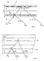
- a section of a one-sided double or multi-reflective information carrier is shown.
- An intermediate layer 3 is embedded between connection media 2 o and 2 u .
- the intermediate layer 3 comprises a dielectric layer 1 and a spacer layer 5.
- the latter preferably consists of a lacquer, in particular a UV-curable, such as a 2P lacquer from the company Philips.
- the dielectric layer 1 consists with a first preference priority at least substantially Si x C y H z and / or Si v N w H u , preferably one of these materials, in the second of Si x C y and / or Si v N w or in third, ZrN or at least substantially HfN or TiN. In the third priority, ZrN is preferred.
- medium 2 u and layer 1 It form medium 2 u and layer 1, the one interface 3 u , medium 2 o and spacer layer 5, the second 3 o .
- An informative structure can be applied or introduced at these two boundary surfaces by local modulation of surface properties, eg for optical information carriers of the geometric structure or for magneto-optical carriers of the magnetic properties.
- the informative structure is shown in principle in FIG. 1 by the regions 7.
- the modulated solid state property ie, as mentioned, for example, geometric surface structuring or magnetic surface structuring, modulates incident electromagnetic radiation 9 upon its relative displacement along the interfaces 3 o , 3 u , as is well known to those skilled in the art.
- the electromagnetic radiation 9 with an intensity I o is reflected on the one hand at the one interface 3 u , corresponding to a reflected portion I o ⁇ R 2 , wherein R 2 indicates the reflection factor.
- This component I o.T 2 passes through the spacer layer 5 virtually without loss and is reflected, corresponding to the factor R 1 , corresponding to the component I o.R 1 .T 2 .
- the transmission T 2 as a quadratic term T 2 2 is included in the expression for I 1 .
- the energy distributions are approximations in which the negligible influence of the optically inactive spacer layer 5 is not taken into account.
- the exact distributions can be determined using the program "Film * STAR", Optical Thin Film Software, FTG Software Associates, P.O. Box 579, Princeton, N.J. 08542, to be calculated.
- the layer 1 used in accordance with the invention is preferably at least predominantly composed of Si x C y , Si x C y H y , Si v N w or Si v N w H u .
- the layer 1 further preferably consists at least predominantly of one of the materials mentioned, but it may also consist at least predominantly of at least two of these four materials mentioned.
- the inventively provided layer 1 preferably from Si x C y and / or Si v N w or, even more preferably, from Si x C y H z and or Si v N w H u .
- D m ⁇ ⁇ O / 4 .
- m ⁇ 1 is integer and odd but can be reduced by up to 0.6 or by up to 0.2.
- ⁇ o is the optical wavelength of the radiation 9 in the intermediate layer material, ie in particular in the material of the layer 1.
- the reflection distribution along the interface 3 o is much less sensitive to thickness variations corresponding to D G of the layer 1 on the material phase 2 u , which in turn leads to a significant advantage in the production of the layer 1.
- the spacer layer 5 is, in particular in optical information carriers, preferably realized by a structurable paint, such as a paint "2P" from Philips, so by means of sheets, the UV ( ⁇ s ⁇ 400 nm) hardened.
- a structurable paint such as a paint "2P” from Philips
- the layer 1 constructed according to the invention in itself already ensures a high transmission (low absorption) in the UV range, which, however, is substantially increased by the mentioned possibility of reducing the layer thickness D G without reflection.
- a transmission for radiation in the UV range is achieved, which is at least 10%.
- the intermediate layer 3, in particular in the case of optical information carriers, is usually deposited on a plastic, in particular on structured polycarbonate or PMMA, as connection medium 2 u .
- n 1 is required on the layer material, namely because the refractive index of the mentioned substrate material is already high, for polycarbonate, for example, about 1.57. If, on the other hand, the refractive index n 1 is increased in the layer materials used, this leads to a lowering of the transmission T 2 , ie to an increase in the absorption in the material of the layer 1.
- the signal obtained from the interface 3 o according to FIG. 1, however, is very high sensitive to a decrease in the transmission T 2 (increase in absorption) dependent.
- Si x C y H z can be optimally taken into account by varying two parameters, namely the carbon content y and the hydrogen content z, the aforementioned contradictory requirements. How this manufacturing technology is achieved, will be carried out later on the basis of the manufacturing process.
- reflection values R 2 (635nm) of polycarbonate as phase 2 u from 20% to 40% reach.
- the reflection R 1 is optimized by selection of the medium 2 o according to FIG. 1 and was, for example , 81% of the energy impinging on the second boundary surface for Al as the material of phase 2 o .
- the inventive intermediate layers 3 or layers 1 can also be used successfully for radiation in the blue region, ie with wavelengths 400 nm ⁇ ⁇ s ⁇ 500 nm.
- the layer formed according to the invention, as described above can be used to selectively use different wavelengths of radiation, such as 635nm and 785nm, to selectively provide information at one interface with one wavelength radiation from the second interface by radiation of the second wavelength read. If, for example, with reference to FIG.
- the optically active layer becomes 1 designed so that almost all of the energy at 635 nm is reflected at R 2 and virtually all the energy at 785 nm is transmitted to the interface 3 o and reflected there.
- This is realized by designing the geometric thickness D G of the layer 1 to be designed on the basis of an odd number of quarter wavelengths corresponding to 635nm, but at the same time based on an even number of quarter wavelengths at 785nm.
- layer 1 With respect to polycarbonate, and most likely to PMMA on the one hand, and most probably to UV curable paints, layer 1, with respect to adhesion, meets the adhesion tape tests according to MIL-M-13508C and / or MIL-C-00675B, as described in H. Pulker, "Coatings on Glass", p. 358, Elsevier, 1984.
- an optical information carrier formed as an optical disk with two information interfaces 3 o ', 3 u '.
- a layer 1 is deposited, according to the preferred information under 1) to 3.8).
- a metallic reflection layer 2 o 'of Au or Ag, but preferably of Al is provided on the spacer layer 5.
- the highly reflective layer 2 o ' is covered with a cover layer 2 oD .
- each of the three interfaces 3 u , 3 o1 , 3 o2 preferably just again reflected at a laser light wavelength of 635 nm, so much that the read-out rays S 1 to S 3 each contain about 20% of the incident energy I.
- the absorption per "semipermeable" layer 1 is less than 2% and correspondingly high is the respective T 2 .
- SD Super Density Disk
- the "semipermeable" layer 1 (FIGS. 1 to 3) is deposited by ion plating, while in the preferred system configuration according to FIG. 5, in a preferred manner, the deposited layer 1 is coated by reactive sputtering is filed.
- the cited layers on the information carriers according to the invention also to be of a different kind and to produce - on the one hand, as a first important aspect, the ratio of transmission T 2 and refractive index n 1 at the preferably used Si x C y H z - and / or Si v N w H u layer by guiding the ratio of carbon optimized to hydrogen. This is preferably done by controlled or regulated feeding of at least two gases with different C / H or N / H fractions into the process atmosphere.
- Si atoms are liberated from high-purity silicon as a solid in the process atmosphere and reacted there with carbon, preferably carbon and hydrogen-containing gas.
- carbon preferably carbon and hydrogen-containing gas.
- the first aspect makes it possible, by guiding the proportions of the gases mentioned in the process atmosphere, to optimize the optical conditions, and the second, to use a cost-effective, easily controllable process.
- a noble gas e.g. Ar
- hydrocarbon gases such as butane C 4 H 10 , methane CH 4 , propane C 3 H 8 , nitrogen N 2 or nitrogen-hydrogen gases, which by controlling or regulating the gas flows in the process atmosphere more or less carbon C or nitrogen N be admitted per unit time in the process atmosphere, based on the hydrogen, which is admitted per unit time.
- Si from a Si solid-state source results in much less expensive solid-state sources than, for example, the release of SiC from known graphite-doped silicon sources. Due to the precisely defined solid state composition of the silicon at the solid source, the entire coating process is better controllable and, by varying the process gas composition, feasible.
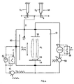
- a Ionenplattierstrom shows, in a vacuum chamber 51, between electrode 53 and 54, a plasma discharge PL is operated.
- silicon of a target 55 is vaporized or atomized into the process atmosphere.
- a discharge PL can of course, and as known in the art, the silicon by thermal evaporation, such as by electron beam evaporation, are released into the process atmosphere.
- the discharge PL is operated by means of a DC source 57.
- this is realized in that the two discharge electrodes 53/54 are intermittently connected via a chopper unit 59 high impedance / low resistance, which is shown in dashed lines. This is done with a predetermined fixed repetition rate or duty cycle and / or preferably in that the generation of interference discharges in the process space is automatically registered and immediately thereafter, with the chopper unit 59, the mentioned electrodes are connected to low impedance as needed.
- a workpiece support electrode 60 which is e.g. with respect to electrode 54 is set to a negative DC potential by means of a DC source 62, wherein the stability of the coating process on the workpiece support electrode 60 is ensured here by means of superposition of the type described, preferably by means of a chopper unit 64 called (59).
- a chopper unit 64 called (59).
- the electrodes 53, 54 and 60 the person skilled in the art is well aware of various possibilities, including the determination of a reference potential, namely of ground potential.
- a reactive gas G with carbon C and / or nitrogen N 2 is generated by controlled mixing of two gases G 1 and G 2 , as shown schematically with the controllable valves V 1 and V 2 .
- the ratio C / H can be controlled by controlling different proportions of the gases G 1 / G 2 in the process atmosphere or N / H at the depositing Si x C y H z or Si v N w H u layer are controlled and thus, by means of two independent parameters, C and H or N and H, the transmission T 2 and the refractive value n 1 at the resulting Si x C y H z - or Si v N w H u layer.
- propane is preferably used for Si x C y H z and nitrogen for Si v N w .
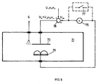
- FIG. 5 shows, for example and schematically a plant for this purpose.
- the silicon is released into the process atmosphere of the vacuum recipient 71 from a magnetron source 70.
- the magnetron electrode 70 is connected to the workpiece support electrode 73 via a DC source 75 of the type described above, again employing a previously discussed chopper assembly 77, shown in phantom, as the preferred realization of the superposition 78 at the DC voltage and an AC voltage, preferably one Mf or Tf voltage, preferably a pulsating.
- a silicon target is used which is n- or p-doped, preferably with boron and / or phosphorus.
- the resistivity of the target material of the doped Si, ⁇ Si 0 . 01 ⁇ .OMEGA.cm ⁇ ⁇ si ⁇ 6 ⁇ .OMEGA.cm ,
- This procedure allows a cost-effective operation at a high deposition rate, whereby the silicon without unwanted arcing and spattering, resulting in a high layer quality, is dusted.
- the reactive gas G is introduced as a single gas or as a gas mixture, as has already been explained with reference to FIG. 4.
- the layers may be deposited with the magnetron source 70 in a known manner, for example by placing the substrate directly in front of the target, or by passing on the target, e.g. in linear continuous systems or in systems with rotating, cylindrical workpiece carriers.
- a Si x C y H z layer was deposited.
- a system was used, as shown in principle in Fig. 5.
- the substrates were mounted on a cylinder support and were moved past a rectangular magnetron.
- the substrate / target distance was 70mm.
- Power supply 10kW / DC with chopper unit (77, Fig. 5);
- Working gas Ar;
- Reactive gas Propane, C 3 H 8 ; Reactive Mode / Metal Mode: Control by plasma emission monitor measurement and intervention on chopper (77) and on Ar / C 3 H 8 flow controller (V1 / V2 of Fig. 4);
- Discharge power 7kW; Rotational frequency of the workpiece carrier electrode (73): 0.5 Hz.
- the following table specifies the further process parameters set for the coating process for three batches no. 2, 3, 4. charge power Argon flow gas pressure Metal mode voltage Reactive mode voltage Propane River flow ratio sputtering kW sccm e-3 mbar UMM URM qC3H8 qC3H8: QAR V V sccm s 2 7 25.5 4 807 777-780 5.9 23:14% 377 3 7 25.5 4 800 724 12 47.06% 377 4 7 25.5 4 828 765 11.4 44.71% 225
- Si x C y H z , Si x C y , Si v N w H u and Si v N w layers were deposited on polycarbonate substrates. Although a system as shown in Figure 5 could have been used, an SDS 100 system from Balzers was used where the substrates are held stationary with respect to the target. Substrate / target distance: 40mm Approximate reaction volume: 5000cm 3 Target material: as in Example 1. Power supply: as in Example 1. Working gas: as in Example 1. Reactive gas: Methane for Si x C y and Si x C y H z . Nitrogen and ammonia for: Si v N w and Si v N w H u . Discharge power: 4kW.
- Table 3 shows the corresponding stoichiometries for the postulated refractive index limits that can be used for digital video disk applications.
Landscapes
- Chemical & Material Sciences (AREA)
- Engineering & Computer Science (AREA)
- Chemical Kinetics & Catalysis (AREA)
- Materials Engineering (AREA)
- Mechanical Engineering (AREA)
- Metallurgy (AREA)
- Organic Chemistry (AREA)
- Manufacturing & Machinery (AREA)
- Inorganic Chemistry (AREA)
- Optical Record Carriers And Manufacture Thereof (AREA)
- Manufacturing Optical Record Carriers (AREA)
- Physical Vapour Deposition (AREA)
Applications Claiming Priority (4)
| Application Number | Priority Date | Filing Date | Title |
|---|---|---|---|
| CH2495/95 | 1995-09-01 | ||
| CH249595 | 1995-09-01 | ||
| US674019 | 1996-07-01 | ||
| US08/674,019 US5965228A (en) | 1995-09-01 | 1996-07-01 | Information carrier, method for producing same |
Publications (2)
| Publication Number | Publication Date |
|---|---|
| EP0762406A1 EP0762406A1 (de) | 1997-03-12 |
| EP0762406B1 true EP0762406B1 (de) | 2007-06-06 |
Family
ID=25690592
Family Applications (1)
| Application Number | Title | Priority Date | Filing Date |
|---|---|---|---|
| EP96113620A Expired - Lifetime EP0762406B1 (de) | 1995-09-01 | 1996-08-26 | Informationsträger und Verfahren zu dessen Herstellung |
Country Status (5)
| Country | Link |
|---|---|
| US (1) | US5965228A (enExample) |
| EP (1) | EP0762406B1 (enExample) |
| JP (1) | JPH09265659A (enExample) |
| DE (1) | DE59611433D1 (enExample) |
| WO (1) | WO1997009715A1 (enExample) |
Families Citing this family (8)
| Publication number | Priority date | Publication date | Assignee | Title |
|---|---|---|---|---|
| KR19990011140A (ko) * | 1997-07-21 | 1999-02-18 | 윤종용 | 광디스크 |
| US5879773A (en) * | 1997-11-17 | 1999-03-09 | Eastman Kodak Company | Recordable optical disks with dielectric interlayer |
| DE50006607D1 (de) * | 1999-05-14 | 2004-07-01 | Unaxis Balzers Ag | Verfahren zum herstellen von hybrid-disks und hybrid-disk |
| JP2003051140A (ja) * | 2001-08-06 | 2003-02-21 | Sanyo Electric Co Ltd | 光ディスクおよびその製造方法 |
| JP2006040618A (ja) * | 2004-07-23 | 2006-02-09 | Nissan Motor Co Ltd | 燃料電池システム |
| US20070007357A1 (en) * | 2005-07-08 | 2007-01-11 | Oc Oerlikon Balzers Ag | Wavelength-selective metal dielectric filter and its application to optical discs |
| KR101046520B1 (ko) | 2007-09-07 | 2011-07-04 | 어플라이드 머티어리얼스, 인코포레이티드 | 내부 챔버 상의 부산물 막 증착을 제어하기 위한 pecvd 시스템에서의 소스 가스 흐름 경로 제어 |
| JP5146209B2 (ja) * | 2008-09-11 | 2013-02-20 | 株式会社リコー | 画像形成装置 |
Family Cites Families (21)
| Publication number | Priority date | Publication date | Assignee | Title |
|---|---|---|---|---|
| DE592174C (de) * | 1934-02-02 | Franziska Vornehm Geb Landsman | Vorrichtung zum Reinigen von Bierleitungen | |
| DE564789C (de) * | 1929-12-22 | 1932-11-23 | Sulzer Akt Ges Geb | Kreiselpumpe zum Vorwaermen von Fluessigkeit, insbesondere von Speisewasser |
| DE658885C (de) * | 1934-05-01 | 1938-04-14 | Alois Hauck | Vorrichtung zum Dichten von Fugen an Fenstern, Tueren u. dgl. |
| US3629088A (en) * | 1968-07-11 | 1971-12-21 | Sperry Rand Corp | Sputtering method for deposition of silicon oxynitride |
| NL8200415A (nl) * | 1982-02-04 | 1983-09-01 | Philips Nv | Optische uitleesbare informatieschijf. |
| JPS593017A (ja) * | 1982-06-29 | 1984-01-09 | Sharp Corp | アモルフアスシリコンカ−バイド膜の製造方法 |
| JPH0823941B2 (ja) * | 1988-11-08 | 1996-03-06 | パイオニア株式会社 | 光学式情報記録担体及びその製造方法 |
| EP0372517A3 (en) * | 1988-12-07 | 1990-09-05 | Tosoh Corporation | Magneto-optical recording medium and process for production of the same |
| DE69020393T2 (de) * | 1989-03-20 | 1995-12-21 | Tosoh Corp | Magnetooptischer Aufzeichnungsträger und Verfahren zu seiner Herstellung. |
| EP0410575B1 (en) * | 1989-07-28 | 1995-01-11 | Minnesota Mining And Manufacturing Company | Magneto optic recording medium with hydrogenated silicon carbide dielectric |
| JPH04106742A (ja) * | 1990-08-27 | 1992-04-08 | Shin Etsu Chem Co Ltd | 光磁気記録媒体 |
| US5346740A (en) * | 1990-09-25 | 1994-09-13 | Matsushita Electric Industrial Co., Ltd. | Optical information recording medium |
| JPH05128588A (ja) * | 1991-05-16 | 1993-05-25 | Canon Inc | 光記録媒体、光記録方法及び再生方法、情報書込み装置及び情報レコードの再生装置 |
| US5255262A (en) * | 1991-06-04 | 1993-10-19 | International Business Machines Corporation | Multiple data surface optical data storage system with transmissive data surfaces |
| CH689767A5 (de) * | 1992-03-24 | 1999-10-15 | Balzers Hochvakuum | Verfahren zur Werkstueckbehandlung in einer Vakuumatmosphaere und Vakuumbehandlungsanlage. |
| DE69330702T2 (de) * | 1992-10-05 | 2002-07-11 | Canon K.K., Tokio/Tokyo | Verfahren zur Herstellung eines optischen Speichermediums, Zerstäubungsmethode |
| TW273616B (enExample) * | 1993-12-15 | 1996-04-01 | Ibm | |
| US5540966A (en) * | 1994-08-05 | 1996-07-30 | Minnesota Mining And Manufacturing Company | Dual layer optical medium having partially reflecting thin film layer |
| US5414678A (en) * | 1994-09-02 | 1995-05-09 | Minnesota Mining And Manufacturing Company | Magneto-optic recording medium having two recording layers, and drive for same |
| JPH08235641A (ja) * | 1995-02-27 | 1996-09-13 | Sony Corp | 光学記録媒体とその製法 |
| WO1997014145A1 (en) * | 1995-10-13 | 1997-04-17 | Philips Electronics N.V. | Optical registration medium with dual information layer |
-
1996
- 1996-07-01 US US08/674,019 patent/US5965228A/en not_active Expired - Fee Related
- 1996-08-26 DE DE59611433T patent/DE59611433D1/de not_active Expired - Lifetime
- 1996-08-26 EP EP96113620A patent/EP0762406B1/de not_active Expired - Lifetime
- 1996-08-30 JP JP8230279A patent/JPH09265659A/ja active Pending
- 1996-09-02 WO PCT/CH1996/000299 patent/WO1997009715A1/de not_active Ceased
Also Published As
| Publication number | Publication date |
|---|---|
| EP0762406A1 (de) | 1997-03-12 |
| JPH09265659A (ja) | 1997-10-07 |
| US5965228A (en) | 1999-10-12 |
| WO1997009715A1 (de) | 1997-03-13 |
| DE59611433D1 (de) | 2007-07-19 |
Similar Documents
| Publication | Publication Date | Title |
|---|---|---|
| DE69313926T2 (de) | Optisches Aufzeichungsmedium und Verfahren zur Herstellung desselben | |
| EP0326935B1 (de) | Verfahren zur Herstellung einer dünnen röntgenamorphen Aluminiumnitrid- oder Aluminium-siliciumnitridschicht auf einer Oberfläche | |
| DE69022497T2 (de) | Optisches Aufzeichnungsmedium. | |
| DE60037045T2 (de) | Optisches Aufzeichnungsmedium und Herstellungsverfahren dafür | |
| DE69219051T2 (de) | Optisches aufzeichnungsmedium und verfahren zu dessen herstellung | |
| DE3905625C2 (de) | Verfahren zur Herstellung eines magnetoresistiven Magnetkopfes | |
| DE19916051C2 (de) | Aufzeichnungsmedium | |
| EP0762406B1 (de) | Informationsträger und Verfahren zu dessen Herstellung | |
| DE60033017T2 (de) | Halbleiterlaser, verfahren zu dessen herstellung und optische plattenvorrichtung | |
| DE3534571A1 (de) | Lichtaufzeichnungsmaterial | |
| DE3413086A1 (de) | Ferrimagnetische oxide und diese enthaltende magneto-optische aufzeichnungsmaterialien | |
| DE69417806T2 (de) | Magnetooptischer Aufzeichnungsträger | |
| DE3030434C2 (de) | Laserstrahlaufzeichnungsträger und Verfahren zu dessen Herstellung | |
| DE69330702T2 (de) | Verfahren zur Herstellung eines optischen Speichermediums, Zerstäubungsmethode | |
| DE112006003218T5 (de) | Filmherstellvorrichtung und Verfahren zum Herstellen eines Films | |
| DE102013112532A1 (de) | Strahlungsabsorber zum Absorbieren elektromagnetischer Strahlung, Solarabsorber-Anordnung, und Verfahren zum Herstellen eines Strahlungsabsorbers | |
| EP0326933B1 (de) | Verfahren zur Herstellung eines flächenförmigen, mehrschichtigen magneto-optischen Aufzeichnungsmaterials | |
| DE69225571T2 (de) | Substrat für optisches Aufzeichnungsmedium und magneto-optisches Aufzeichnungsmedium mit einem solchen Substrat | |
| DE3803014A1 (de) | Verfahren zur herstellung einer duennen roentgenamorphen aluminiumnitrid- oder aluminiumsiliciumnitrid-schicht auf einer oberflaeche | |
| DE19528329A1 (de) | Röntgenstrahlendurchlässiges Schichtmaterial, Verfahren zu seiner Herstellung sowie deren Verwendung | |
| EP0410337A2 (de) | Schutzschichten aus Keramiken des Germaniums | |
| DE3309483C3 (de) | Magnetooptisches Aufzeichnungsmaterial und dessen Verwendung | |
| DE29614938U1 (de) | Informationsträger und Anlage zur Schichtherstellung | |
| EP0446784A2 (de) | Magnetooptische Datenplatte | |
| DE69013695T2 (de) | Verfahren zur Aufnahme und Wiedergabe von Information. |
Legal Events
| Date | Code | Title | Description |
|---|---|---|---|
| PUAI | Public reference made under article 153(3) epc to a published international application that has entered the european phase |
Free format text: ORIGINAL CODE: 0009012 |
|
| AK | Designated contracting states |
Kind code of ref document: A1 Designated state(s): CH DE FR GB LI NL |
|
| 17P | Request for examination filed |
Effective date: 19970610 |
|
| 17Q | First examination report despatched |
Effective date: 20000127 |
|
| RAP1 | Party data changed (applicant data changed or rights of an application transferred) |
Owner name: UNAXIS BALZERS AKTIENGESELLSCHAFT |
|
| RTI1 | Title (correction) |
Free format text: INFORMATION CARRIER AND MANUFACTURING METHOD THEREOF |
|
| RTI1 | Title (correction) |
Free format text: INFORMATION CARRIER AND MANUFACTURING METHOD THEREOF |
|
| GRAP | Despatch of communication of intention to grant a patent |
Free format text: ORIGINAL CODE: EPIDOSNIGR1 |
|
| RAP1 | Party data changed (applicant data changed or rights of an application transferred) |
Owner name: OC OERLIKON BALZERS AG |
|
| GRAS | Grant fee paid |
Free format text: ORIGINAL CODE: EPIDOSNIGR3 |
|
| GRAA | (expected) grant |
Free format text: ORIGINAL CODE: 0009210 |
|
| AK | Designated contracting states |
Kind code of ref document: B1 Designated state(s): CH DE FR GB LI NL |
|
| RAP1 | Party data changed (applicant data changed or rights of an application transferred) |
Owner name: OC OERLIKON BALZERS AG |
|
| REG | Reference to a national code |
Ref country code: GB Ref legal event code: FG4D Free format text: NOT ENGLISH |
|
| REG | Reference to a national code |
Ref country code: CH Ref legal event code: EP |
|
| REF | Corresponds to: |
Ref document number: 59611433 Country of ref document: DE Date of ref document: 20070719 Kind code of ref document: P |
|
| NLV1 | Nl: lapsed or annulled due to failure to fulfill the requirements of art. 29p and 29m of the patents act | ||
| GBV | Gb: ep patent (uk) treated as always having been void in accordance with gb section 77(7)/1977 [no translation filed] |
Effective date: 20070606 |
|
| PG25 | Lapsed in a contracting state [announced via postgrant information from national office to epo] |
Ref country code: NL Free format text: LAPSE BECAUSE OF FAILURE TO SUBMIT A TRANSLATION OF THE DESCRIPTION OR TO PAY THE FEE WITHIN THE PRESCRIBED TIME-LIMIT Effective date: 20070606 |
|
| EN | Fr: translation not filed | ||
| REG | Reference to a national code |
Ref country code: CH Ref legal event code: PUE Owner name: OERLIKON TRADING AG, TRUEBBACH Free format text: OC OERLIKON BALZERS AG#IRAMALI 18#9496 BALZERS (LI) -TRANSFER TO- OERLIKON TRADING AG, TRUEBBACH#HAUPTSTRASSE#9477 TRUEBBACH (CH) |
|
| PLBE | No opposition filed within time limit |
Free format text: ORIGINAL CODE: 0009261 |
|
| STAA | Information on the status of an ep patent application or granted ep patent |
Free format text: STATUS: NO OPPOSITION FILED WITHIN TIME LIMIT |
|
| PG25 | Lapsed in a contracting state [announced via postgrant information from national office to epo] |
Ref country code: GB Free format text: LAPSE BECAUSE OF FAILURE TO SUBMIT A TRANSLATION OF THE DESCRIPTION OR TO PAY THE FEE WITHIN THE PRESCRIBED TIME-LIMIT Effective date: 20070606 |
|
| 26N | No opposition filed |
Effective date: 20080307 |
|
| PG25 | Lapsed in a contracting state [announced via postgrant information from national office to epo] |
Ref country code: FR Free format text: LAPSE BECAUSE OF FAILURE TO SUBMIT A TRANSLATION OF THE DESCRIPTION OR TO PAY THE FEE WITHIN THE PRESCRIBED TIME-LIMIT Effective date: 20080201 |
|
| REG | Reference to a national code |
Ref country code: CH Ref legal event code: PUE Owner name: SINGULUS TECHNOLOGIES AG Free format text: OERLIKON TRADING AG, TRUEBBACH#HAUPTSTRASSE#9477 TRUEBBACH (CH) -TRANSFER TO- SINGULUS TECHNOLOGIES AG#HANAUER LANDSTRASSE 103#63796 KAHL AM MAIN (DE) Ref country code: CH Ref legal event code: NV Representative=s name: VOSSIUS & PARTNER |
|
| PGFP | Annual fee paid to national office [announced via postgrant information from national office to epo] |
Ref country code: CH Payment date: 20100830 Year of fee payment: 15 |
|
| PGFP | Annual fee paid to national office [announced via postgrant information from national office to epo] |
Ref country code: DE Payment date: 20100929 Year of fee payment: 15 |
|
| REG | Reference to a national code |
Ref country code: CH Ref legal event code: PL |
|
| PG25 | Lapsed in a contracting state [announced via postgrant information from national office to epo] |
Ref country code: CH Free format text: LAPSE BECAUSE OF NON-PAYMENT OF DUE FEES Effective date: 20110831 Ref country code: LI Free format text: LAPSE BECAUSE OF NON-PAYMENT OF DUE FEES Effective date: 20110831 |
|
| REG | Reference to a national code |
Ref country code: DE Ref legal event code: R119 Ref document number: 59611433 Country of ref document: DE Effective date: 20120301 |
|
| PG25 | Lapsed in a contracting state [announced via postgrant information from national office to epo] |
Ref country code: DE Free format text: LAPSE BECAUSE OF NON-PAYMENT OF DUE FEES Effective date: 20120301 |