EP0759618B1 - Halbleiterspeicheranordnung mit segmentierter Dekodierschaltung mit NMOS-Transistoren - Google Patents
Halbleiterspeicheranordnung mit segmentierter Dekodierschaltung mit NMOS-Transistoren Download PDFInfo
- Publication number
- EP0759618B1 EP0759618B1 EP96112536A EP96112536A EP0759618B1 EP 0759618 B1 EP0759618 B1 EP 0759618B1 EP 96112536 A EP96112536 A EP 96112536A EP 96112536 A EP96112536 A EP 96112536A EP 0759618 B1 EP0759618 B1 EP 0759618B1
- Authority
- EP
- European Patent Office
- Prior art keywords
- word line
- address signal
- row address
- transistor
- mos transistor
- Prior art date
- Legal status (The legal status is an assumption and is not a legal conclusion. Google has not performed a legal analysis and makes no representation as to the accuracy of the status listed.)
- Expired - Lifetime
Links
Images

Classifications
-
- G—PHYSICS
- G11—INFORMATION STORAGE
- G11C—STATIC STORES
- G11C11/00—Digital stores characterised by the use of particular electric or magnetic storage elements; Storage elements therefor
- G11C11/21—Digital stores characterised by the use of particular electric or magnetic storage elements; Storage elements therefor using electric elements
- G11C11/34—Digital stores characterised by the use of particular electric or magnetic storage elements; Storage elements therefor using electric elements using semiconductor devices
- G11C11/40—Digital stores characterised by the use of particular electric or magnetic storage elements; Storage elements therefor using electric elements using semiconductor devices using transistors
- G11C11/401—Digital stores characterised by the use of particular electric or magnetic storage elements; Storage elements therefor using electric elements using semiconductor devices using transistors forming cells needing refreshing or charge regeneration, i.e. dynamic cells
- G11C11/4063—Auxiliary circuits, e.g. for addressing, decoding, driving, writing, sensing or timing
- G11C11/407—Auxiliary circuits, e.g. for addressing, decoding, driving, writing, sensing or timing for memory cells of the field-effect type
- G11C11/408—Address circuits
- G11C11/4085—Word line control circuits, e.g. word line drivers, - boosters, - pull-up, - pull-down, - precharge
-
- G—PHYSICS
- G11—INFORMATION STORAGE
- G11C—STATIC STORES
- G11C8/00—Arrangements for selecting an address in a digital store
- G11C8/10—Decoders
-
- G—PHYSICS
- G11—INFORMATION STORAGE
- G11C—STATIC STORES
- G11C11/00—Digital stores characterised by the use of particular electric or magnetic storage elements; Storage elements therefor
- G11C11/21—Digital stores characterised by the use of particular electric or magnetic storage elements; Storage elements therefor using electric elements
- G11C11/34—Digital stores characterised by the use of particular electric or magnetic storage elements; Storage elements therefor using electric elements using semiconductor devices
- G11C11/40—Digital stores characterised by the use of particular electric or magnetic storage elements; Storage elements therefor using electric elements using semiconductor devices using transistors
- G11C11/401—Digital stores characterised by the use of particular electric or magnetic storage elements; Storage elements therefor using electric elements using semiconductor devices using transistors forming cells needing refreshing or charge regeneration, i.e. dynamic cells
- G11C11/4063—Auxiliary circuits, e.g. for addressing, decoding, driving, writing, sensing or timing
- G11C11/407—Auxiliary circuits, e.g. for addressing, decoding, driving, writing, sensing or timing for memory cells of the field-effect type
- G11C11/408—Address circuits
- G11C11/4087—Address decoders, e.g. bit - or word line decoders; Multiple line decoders
-
- G—PHYSICS
- G11—INFORMATION STORAGE
- G11C—STATIC STORES
- G11C8/00—Arrangements for selecting an address in a digital store
- G11C8/12—Group selection circuits, e.g. for memory block selection, chip selection, array selection
-
- G—PHYSICS
- G11—INFORMATION STORAGE
- G11C—STATIC STORES
- G11C8/00—Arrangements for selecting an address in a digital store
- G11C8/08—Word line control circuits, e.g. drivers, boosters, pull-up circuits, pull-down circuits, precharging circuits, for word lines
Definitions
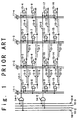
- the present invention relates to a semiconductor memory device, and more particularly to a semiconductor memory device in which word lines are grouped into main word lines and sub-word lines such that the main word line is driven by a main decoder circuit and the sub-word line is driven by a divisional decoder circuit in a DRAM (dynamic RAM).
- DRAM dynamic RAM
- a semiconductor memory device in which word lines are grouped into a group of main word lines 12-1 and 12-2 and a group of sub-word lines 13-1 through 13-16 such that the word lines are hierarchized.
- the main word lines 12-1 and 12-2 are driven by the outputs of main X decoders 14-1 and 14-2, respectively, and the sub-word lines 13-1 through 13-16 are driven by the outputs of divisional decoders 15-1 through 15-16, respectively.
- the main X decoder 14-1 decodes address signals on row address lines 10-1, 10-3, and 10-4 to drive the main word line 12-1, and the main X decoder 14-2 decodes address signals on row address lines 10-2, 10-3, and 10-4 to drive the main word line 12-2.
- the divisional decoder 15-1 decodes signals on the main word line 12-1 and a part of remaining row address lines 11-1 to drive the sub-word line 13-1.
- a divisional decoder 15-2 decodes signals on the main word line 12-1 and a part of remaining row address lines 11-2 to drive the sub-word line 13-2.
- the other divisional decoder 15-3 through 15-16 decode signals on corresponding word lines and corresponding parts of remaining row address lines in the same manner to drive corresponding sub-word lines, respectively, as shown in the figure.
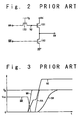
- circuit structure of the divisional decoders 15-1 to 15-16 there are proposed three types of circuit structure and these circuit examples are shown in Figs. 2, 4 and 6, respectively.
- the circuit shown in Fig. 2 is disclosed in "A boosted Dual Word-line Decoding Scheme for 256Mb Drams", (Symposium on VLSI circuits Digest of Technical Papers, pp.112-113, 1992) and is composed of three NMOS transistors 151 to 153.
- the transistor 151 is a drive transistor for driving the sub-word line SW to the potential of a selected state.
- the transistor 152 is a reset transistor for resetting the sub-word line SW to the potential of a non-selected state (the ground potential).
- the transistor 153 is a transfer gate transistor for transferring the potential of a main word line MW to the gate of the drive transistor 151.
- the gate of this transistor 153 is applied with a fixed potential VB enough to make this transistor 153 always turn on and an address signal RA is supplied to the drain of the transistor 151. Also, the gate of the transistor 152 is applied with a signal having a phase inverse to the main address line MW.
- the sub-word line SW is driven by a common connection node of the source of the transistor 151 and the drain of the transistor 152.
- Fig. 3 shows examples of signal wave forms of the respective points of the circuit shown in Fig. 2.
- the potential of the main word line MW is first set to the H level (high level; the power supply voltage level VB) and at the same time, the potential of the inverse phase signal of a signal on the main word line MW is set to the L level (low level; the ground level) (It is shown in Fig. 3 as the inverted MW and the H level is VCC and VCC ⁇ VB is satisfied).
- the address signal RA is set to the H level so that the sub-word line SW is driven to the H level.
- the selected state is achieved.
- the potential of the gate N2 of the transistor 151 is raised higher than the VB level by the operation of the transfer gate transistor 153 (i.e., it is boosted). Therefore, the source potential of the transistor 151, i.e., the potential of the sub-word line SW is sufficiently driven to the H level.
- the potential of the main word line MW is set to the L level and the phase inverted signal is set to the H level.
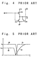
- the circuit shown in Fig. 4 is disclosed-in Nikkei Microdevices (November, 1993) and is composed of the two NMOS transistors 255 and 256 and one PMOS transistor 254.
- the transistor 254 is a drive transistor for driving a sub-word line SW to a selected state.
- the transistor 256 is a reset transistor for resetting the sub-word line SW to a non-selected state.
- the transistor 55 is a floating prevention transistor for preventing floating to the sub-word line SW.
- the gate of the transistor 254 is directly supplied with the potential of the main word line MW and an address signal RA is supplied to the source of the transistor 254.
- the potential of the main word line MW is supplied to the gate of the transistor 255 and the phase inverted signal (inverted RA) of the address signal RA is supplied to the gate of the transistor 256.
- the sub-word line SW is connected to the common drain of the transistors 254 to 256.
- Fig. 5 shows examples of wave forms of respective portions of the circuit shown in Fig. 4.
- the. address signal RA is first set to the H level.
- the phase inverted signal (inverted RA) is set to the L level.
- the potential of the main word line MW is set to the L level.
- the address signal RA is set to the L level and the phase inverted signal is set to the H level.
- the main word line MW is maintained at the H level, thereby the sub-word line SW is maintained at the L level by the transistor 255 which makes it possible to prevent floating.
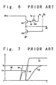
- the circuit shown in Fig. 6 is disclosed in "A 150 MHz 8-Banks 256M Synchronous DRAM with Wave Pipelining Methods" (ISSCC Digest of Technical Papers, pp. 250 - 251, Feb., 1995) and is composed of three NMOS transistors 357 to 359.
- the transistor 357 is a transistor for driving a sub-word line SW to a selected state and the transistor 359 is a transistor for transferring an address signal RA to the gate of the transistor 357.
- the transistor 358 is a transistor for resetting the sub-word line SW to a non-selected state.
- the main word line MW is connected to the drain of the transistor 357 and the phase inverted signal of the address signal RA is applied to the gate of the transistor 358.
- the gate of the transistor 359 is applied with a potential VB enough to make this transistor always turn on and the address signal RA is applied to the drain of this transistor.
- the sub-word line SW is driven by the common connection node of the source of the transistor 357 and the drain of the transistor 358.
- Fig. 7 shows examples of wave forms of the respective portion of the circuit shown in Fig. 6.
- the main word line MW is first set to the H level and then the address signal RA is set to the H level.
- the phase inverted signal is set to the L level.
- the potential N3 of the gate of the transistor 357 is raised higher than the VB level by the operation of the transfer gate transistor 359 (i.e., it is boosted). Therefore, the source potential of the transistor 357, i.e. the potential of the sub-word line SW is sufficiently set to the H level.
- the address signal RA is set to the L level and the phase inverted signal is set to the H level.
- the address signal RA is set to the L level and the phase inverted signal is set to the H level.
- the signal having a phase inverse to a signal on the main word line MW (i.e., an inverted MW) is used. Therefore, there is a problem in that the fault current such as a small leak current between the main word lines MW and the phase inverted signal line, and a short circuit current which is due to the short-circuiting between them can not be relieved.
- An object of the present invention is to provide a semiconductor memory device which can be composed of transistor elements of an identical conductive type, and in which the address signal can be inputted to the drain of the transistor element such that increase of a chip area can be suppressed in case of making the whole circuit as an IC.
- Another object of the present invention is to provide a semiconductor memory device in which a signal having a phase inverse to a signal of a main word line is not used.
- a semiconductor memory device includes a series circuit composed of a drive MOS transistor and a reset MOS transistor connected in series via a common connection node, a source of the reset MOS transistor being connected to a lower potential power supply, a main word line, a sub-word line connected to the common connection node, a row address signal section for decoding a first part of an address signal to generate a first row address signal and a second row address signal having a phase inverse to that of the first row address signal in accordance with the decoding result, and for supplying the first row address signal to a drain of the drive MOS transistor and the second row address signal to a gate of a reset MOS transistor, the address signal including the first part and a second part, a main decoder circuit for decoding the second part of the address signal to output a main word line signal to the main word line in accordance with the decoding result before the row address signal section supplies the first and second row address signals, and a transfer section for transferring the main word line signal to a
- the semiconductor memory device further includes a floating prevention MOS transistor having a gate connected to the first row address signal, a drain connected to the main word line, and a source connected to the common connection node.
- All of the MOS transistor elements have the same conduction type, i.e., is composed of NMOS transistors.
- Fig. 8 is a circuit diagram illustrating the structure of a divisional decoder circuit and its peripheral circuit section of a semiconductor memory device according to the first embodiment of the present invention.
- the divisional decoder circuit is composed of four MMOS transistors 1 to 4.
- the NMOS transistor 2 is a drive transistor for selecting a sub-word line SW and the NMOS transistor 1 is a transfer gate transistor for controlling the potential supply of a main word line MW to the gate of the NMOS transistor 2.
- the NMOS transistor 3 is a reset transistor for the non-selected state of the sub-word line SW and the NMOS transistor 4 is a floating prevention transistor for the non-selected state of the sub-word line SW.
- a main decoder circuit 31 and a row address decoder circuit 32 are provided around of the divisional decoder circuit.
- the main word line MW is connected to the drain of the NMOS transistor 1 and the gate of the NMOS transistor 1 is applied with a fixed voltage VB enough to make the NMOS transistor 1 always turn on, and the source of the NMOS transistor 1 functions as a gate input of the NMOS transistor 2.
- the address signal RA is supplied to the drain of the NMOS transistor 2 and the sub-word line is connected to the source of the NMOS transistor 2.
- the phase inverted signal (inverted RA) of the address signal RA is applied to the gate of the NMOS transistor 3 and the source of the NMOS transistor 3 is grounded.
- the sub-word line SW is connected to the drain of the NMOS transistor 3.
- the main word line MW is also connected to the drain of the NMOS transistor 4.
- the address signal RA is applied to the gate of the NMOS transistor 4.
- the sub-word line SW is connected to the source of the NMOS transistor 4.
- the potential of a main word line is set to an H level to drive the gate of a drive transistor.
- An address signal of the drain of the drive transistor is driven to the H level to drive a sub-word line connected to the source to the H level.
- the address signal is set to the H level and the phase inverted signal is set to the L level, so that the sub-word line is reset to a reset potential by both of a reset transistor and the drive transistor.
- the potential of the main word line and the address signal are both set to the L level and the phase inverted signal of the address signal is set to the H level.
- a floating prevention transistor having been provided is turned on to prevent the sub-word line from floating to maintains the reset state.
- Fig. 9 is a diagram showing wave form examples of signals of the respective points of the circuit section shown in Fig. 8. The operation of the semiconductor memory device will be described in detail with reference to Fig. 9.
- the node N1 which is the gate of the drive transistor 2 is raised (boosted) higher than the VB level by the operation of the transfer gate transistor 1 and, therefore, the source potential of the NMOS transistor 2, i.e., the potential of the sub-word line SW is set to the H level (the VB level) sufficiently.
- the address signal RA is set to the L level and the phase inverted signal is set to the H level.
- the reset transistor 3 is turned on to reset the potential of the sub-word line SW to the ground potential.
- the voltage of the main word line MW is set to the H level.
- the address signal RA is set to the L level and the phase inverted signal is set to the H level.
- the NMOS transistor 2 and the NMOS transistor 3 are both turned on such that the sub-word line SW is connected to the address signal RA of the L level through the NMOS transistor 3. Therefore, the sub-word line SW is held to the reset state.
- the address signal RA is set to the L level and the phase inverted signal is set to the H level, the NMOS transistor 3 is turned on.
- the NMOS transistor 4 is turned off, the sub-word line SW becomes the ground potential through the NMOS transistor 3 and is maintained to the L level.
- the NMOS transistor 4 is turned on. As a result, because the sub-word line SW is connected to the main word line MW of the L level through the NMOS transistor 4, the sub-word line SW is maintained to the L level.
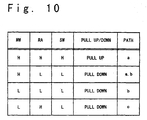
- Fig. 10 shows the relation of logic levels of the main word line MW, the address signal RA, and the sub-word line SW. Also, the pull up or down state of the sub-word line SW in each case and the paths (arrow a-c of dot and dashed lines in Fig. 8) are shown. In this circuit, MOS transistors of the identical conductive type are entirely used. Also, it is not required to use the phase inverted signal of the main word line MW. Further, at the time of any condition, the sub-word line SW never becomes the floating state.
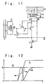
- Fig. 11 is a diagram illustrating the semiconductor memory device according to the second embodiment of the present invention.
- the same components as in Fig. 8 are illustrated with the identical reference numerals. Therefore, only a portion of Fig. 11 which is different from Fig. 8 will be described.
- the gate of the NMOS transistor 1 is connected to the phase inverted signal (inverted RA) of the address signal RA in place of the fixed voltage VB.
- the phase inverted signal is generated by the row address decoder 32 and the high level of the phase inverted signal is boosted to the fixed voltage VB by a boosting circuit 33.
- the other portions are the same as in Fig. 8.
- Fig. 12 is a diagram showing wave form examples of the respective points of the circuit section shown in Fig. 11.
- the potential of the main word line MW is first set to the H level and then the address signal RA is set to the H level. Since the phase inverted signal is set to the H level in an initial state, the gate potential (the potential of N1) of the drive transistor 2 is boosted by the main word line signal. In this case, the phase inverted signal of the address signal becomes the L level at the same time when the address signal RA is set to the H level, the NMOS transistor 1 is turned off. As a result, the gate potential of the NMOS transistor 2 cannot be dropped from the.boosted level, resulting in good efficiency.
- the power supply line VB connected to the gate of the NMOS transistor 1 in Fig. 8 is not required. Therefore, the chip area can be effectively used when the semiconductor memory device is achieved as an IC. The other operations are the same as in Fig. 8.
- the H level of the phase inverted signal of the address signal may be a level sufficient to make the NMOS transistor 3 turn on. Therefore, the H level may be a VCC level (VB > VCC), as shown in Fig. 9.
- the H level of the phase inverted signal of the address signal is made to be VB, as shown in Fig. 5, in order to make the transfer gate NMOS transistor 1 sufficiently turn on such that the gate of the NMOS transistor 2 is sufficiently boosted.
- a divisional decoder is composed of the MOS transistors all having the identical conductive type, i.e., NMOS transistors. Therefore, any element separating region is not required. Also, the phase inverted signal of the main word line is not used. Therefore, the problem on leak current is solved. Further, it is made possible to input the address signal to the drain of the NMOS transistor. Therefore, the load of the address signal is small. Further, because the floating prevention transistor is provided between the main word line and the sub-word line. Therefore, there is no case of floating of the sub-word line.
Claims (6)
- Halbleiterspeichervorrichtung, die aufweist:eine Reihenschaltung (2, 3), die sich aus einem Treiber-MOS-Transistor (2) und einem Rückstell-MOS-Transistor (3) zusammensetzt, die in Reihe über einen gemeinsamen Verbindungsknoten verbunden sind, wobei eine Source des Rückstell-MOS-Transistors mit einer Niedrigpotential-Stromversorgung verbunden ist;eine Hauptwortleitung (MW);eine Unterwortleitung (SW), die mit dem gemeinsamen Verbindungsknoten verbunden ist;eine Zeilenadresssignaleinrichtung (32) zum Decodieren eines ersten Teils (22) eines Adresssignals, um ein erstes Zeilenadresssignal (RA) und ein zweites Zeilenadresssignal (invertiertes RA) mit einer zum ersten Zeilenadresssignal invertierten Phase gemäß dem Decodierergebnis zu erzeugen, und zum Liefern des ersten Zeilenadresssignals an eine Drain des Treiber-MOS-Transistors (2) und des zweiten Zeilenadresssignals an ein Gate des Rückstell-MOS-Transistors (3), wobei das Adresssignal den ersten und einen zweiten Teil umfasst;eine Hauptdecoderschaltung (31) zum Decodieren des zweiten Teils des Adresssignals, um ein Hauptwortleitungssignal an die Hauptwortleitung gemäß dem Decodierergebnis auszugeben, bevor die Zeilenadresssignaleinrichtung (32) das erste und zweite Zeilenadresssignal liefert;eine Transfereinrichtung (1) zum Transferieren des Hauptwortleitungssignals an ein Gate des Treiber-MOS-Transistors; undeinen Schutz-MOS-Transistor (4), der aufweist: ein Gate, das mit dem ersten Zeilenadresssignal verbunden ist, eine Drain, die mit der Hauptwortleitung verbunden ist, und eine Source, die mit dem gemeinsamen Verbindungsknoten verbunden ist.
- Halbleitervorrichtung gemäß Anspruch 1, wobei die Zeilenadresssignaleinrichtung (32) ferner eine Einrichtung (33) zum Verstärken eines Hochpegels des zweiten Zeilenadresssignals auf eine verstärkte Spannung umfasst, die höher als ein höhere Hochpotential-Stromversorgung ist.
- Halbleiterspeichervorrichtung gemäß Anspruch 2, wobei die Transfereinrichtung (1) ferner einen Transfer-MOS-Transistor umfasst, der aufweist: ein Gate, das mit dem zweiten Zeilenadresssignal verbunden ist, eine Drain, die mit der Hauptwortleitung verbunden ist, und eine Source, die mit einem Gate des Treiber-MOS-Transistors verbunden ist.
- Halbleiterspeichervorrichtung gemäß Anspruch 1, wobei die Transfereinrichtung ferner einen Transfer-MOS-Transistor umfasst, der aufweist: ein Gate, das mit einer vorgegebenen Spannung (VB) verbunden ist, die höher als eine Hochpotential-Stromversorgung ist, eine Drain, die mit der Hauptwortleitung verbunden ist, und eine Source, die mit einem Gate des Treiber-MOS-Transistors verbunden ist.
- Halbleiterspeichervorrichtung gemäß einem der Ansprüche 1 bis 4, wobei alle MOS-Transistor-Elemente vom selben Leitungstyp sind.
- Halbleiterspeichervorrichtung gemäß Anspruch 5, wobei alle MOS-Transistoren NMOS-Transistoren sind.
Applications Claiming Priority (3)
| Application Number | Priority Date | Filing Date | Title |
|---|---|---|---|
| JP20894795 | 1995-08-17 | ||
| JP208947/95 | 1995-08-17 | ||
| JP7208947A JP2800730B2 (ja) | 1995-08-17 | 1995-08-17 | 半導体記憶装置 |
Publications (3)
| Publication Number | Publication Date |
|---|---|
| EP0759618A2 EP0759618A2 (de) | 1997-02-26 |
| EP0759618A3 EP0759618A3 (de) | 1998-06-24 |
| EP0759618B1 true EP0759618B1 (de) | 2001-11-14 |
Family
ID=16564784
Family Applications (1)
| Application Number | Title | Priority Date | Filing Date |
|---|---|---|---|
| EP96112536A Expired - Lifetime EP0759618B1 (de) | 1995-08-17 | 1996-08-02 | Halbleiterspeicheranordnung mit segmentierter Dekodierschaltung mit NMOS-Transistoren |
Country Status (6)
| Country | Link |
|---|---|
| US (1) | US5652731A (de) |
| EP (1) | EP0759618B1 (de) |
| JP (1) | JP2800730B2 (de) |
| KR (1) | KR100194572B1 (de) |
| DE (1) | DE69616908T2 (de) |
| TW (1) | TW409258B (de) |
Families Citing this family (9)
| Publication number | Priority date | Publication date | Assignee | Title |
|---|---|---|---|---|
| KR100200724B1 (ko) * | 1996-08-21 | 1999-06-15 | 윤종용 | 반도체 메모리장치의 서브 워드라인 드라이버 |
| JP2000149564A (ja) | 1998-10-30 | 2000-05-30 | Mitsubishi Electric Corp | 半導体記憶装置 |
| US6026047A (en) * | 1998-11-03 | 2000-02-15 | Samsung Electronics Co., Ltd. | Integrated circuit memory device with hierarchical work line structure |
| JP3376301B2 (ja) * | 1998-12-04 | 2003-02-10 | 株式会社東芝 | 半導体記憶装置 |
| JP2000243086A (ja) * | 1998-12-24 | 2000-09-08 | Mitsubishi Electric Corp | 半導体記憶装置 |
| DE10007176A1 (de) | 2000-02-17 | 2001-08-30 | Infineon Technologies Ag | Dekodiervorrichtung |
| TW521226B (en) * | 2000-03-27 | 2003-02-21 | Semiconductor Energy Lab | Electro-optical device |
| US7046578B2 (en) * | 2004-08-23 | 2006-05-16 | Micron Technology, Inc. | Method and apparatus for memory device wordline |
| JP2006313620A (ja) * | 2006-06-22 | 2006-11-16 | Matsushita Electric Ind Co Ltd | 半導体集積回路装置の駆動方法 |
Family Cites Families (8)
| Publication number | Priority date | Publication date | Assignee | Title |
|---|---|---|---|---|
| JPH07109701B2 (ja) * | 1987-11-30 | 1995-11-22 | 株式会社東芝 | キャッシュメモリ |
| KR930002574B1 (ko) * | 1990-03-09 | 1993-04-03 | 금성일렉트론 주식회사 | 워드라인 구동회로 |
| JP3024687B2 (ja) * | 1990-06-05 | 2000-03-21 | 三菱電機株式会社 | 半導体記憶装置 |
| US5121358A (en) * | 1990-09-26 | 1992-06-09 | Sgs-Thomson Microelectronics, Inc. | Semiconductor memory with power-on reset controlled latched row line repeaters |
| US5875148A (en) * | 1993-01-29 | 1999-02-23 | Oki Electric Industry Co., Ltd. | Semiconductor memory |
| KR960011206B1 (ko) * | 1993-11-09 | 1996-08-21 | 삼성전자 주식회사 | 반도체메모리장치의 워드라인구동회로 |
| JP2785717B2 (ja) * | 1994-09-30 | 1998-08-13 | 日本電気株式会社 | 半導体記憶装置 |
| JP3781793B2 (ja) * | 1995-01-10 | 2006-05-31 | 株式会社ルネサステクノロジ | ダイナミック型半導体記憶装置 |
-
1995
- 1995-08-17 JP JP7208947A patent/JP2800730B2/ja not_active Expired - Lifetime
-
1996
- 1996-07-23 TW TW085108943A patent/TW409258B/zh not_active IP Right Cessation
- 1996-08-02 EP EP96112536A patent/EP0759618B1/de not_active Expired - Lifetime
- 1996-08-02 US US08/691,591 patent/US5652731A/en not_active Expired - Lifetime
- 1996-08-02 DE DE69616908T patent/DE69616908T2/de not_active Expired - Lifetime
- 1996-08-13 KR KR1019960033540A patent/KR100194572B1/ko not_active IP Right Cessation
Also Published As
| Publication number | Publication date |
|---|---|
| DE69616908T2 (de) | 2002-08-29 |
| EP0759618A3 (de) | 1998-06-24 |
| DE69616908D1 (de) | 2001-12-20 |
| US5652731A (en) | 1997-07-29 |
| JP2800730B2 (ja) | 1998-09-21 |
| KR100194572B1 (ko) | 1999-06-15 |
| JPH0963261A (ja) | 1997-03-07 |
| EP0759618A2 (de) | 1997-02-26 |
| TW409258B (en) | 2000-10-21 |
| KR970012756A (ko) | 1997-03-29 |
Similar Documents
| Publication | Publication Date | Title |
|---|---|---|
| US6269047B1 (en) | Semiconductor memory device | |
| US7541837B2 (en) | Voltage level shifter circuit | |
| US6545923B2 (en) | Negatively biased word line scheme for a semiconductor memory device | |
| EP0199176B1 (de) | Wortlinienspannungserhöhungstakt- und Decodersteuerungsstromkreise in Halbleiterspeichern | |
| US6774673B2 (en) | Level shifter | |
| EP0759618B1 (de) | Halbleiterspeicheranordnung mit segmentierter Dekodierschaltung mit NMOS-Transistoren | |
| US5818790A (en) | Method for driving word lines in semiconductor memory device | |
| US6529439B2 (en) | Semiconductor memory device | |
| US5808482A (en) | Row decoder with level translator | |
| US5369620A (en) | Dynamic random access memory device having column selector for selecting data lines connectable with bit lines | |
| JP3182120B2 (ja) | サブロウデコーダ回路 | |
| US6229755B1 (en) | Wordline driving apparatus in semiconductor memory devices | |
| US5469385A (en) | Output buffer with boost from voltage supplies | |
| US6252808B1 (en) | Semiconductor memory device having improved row redundancy scheme and method for curing defective cell | |
| KR100213215B1 (ko) | 반도체 메모리 장치의 서브 워드라인 드라이버 제어 신호 발생 회로 | |
| KR20000043180A (ko) | 서브 워드라인 디코더 | |
| JPH08171797A (ja) | 半導体記憶装置 | |
| KR19980060862A (ko) | 로오 디코더 회로 |
Legal Events
| Date | Code | Title | Description |
|---|---|---|---|
| PUAI | Public reference made under article 153(3) epc to a published international application that has entered the european phase |
Free format text: ORIGINAL CODE: 0009012 |
|
| AK | Designated contracting states |
Kind code of ref document: A2 Designated state(s): DE FR GB |
|
| PUAL | Search report despatched |
Free format text: ORIGINAL CODE: 0009013 |
|
| AK | Designated contracting states |
Kind code of ref document: A3 Designated state(s): DE FR GB |
|
| 17P | Request for examination filed |
Effective date: 19981022 |
|
| 17Q | First examination report despatched |
Effective date: 20000313 |
|
| GRAG | Despatch of communication of intention to grant |
Free format text: ORIGINAL CODE: EPIDOS AGRA |
|
| GRAG | Despatch of communication of intention to grant |
Free format text: ORIGINAL CODE: EPIDOS AGRA |
|
| GRAH | Despatch of communication of intention to grant a patent |
Free format text: ORIGINAL CODE: EPIDOS IGRA |
|
| GRAH | Despatch of communication of intention to grant a patent |
Free format text: ORIGINAL CODE: EPIDOS IGRA |
|
| GRAA | (expected) grant |
Free format text: ORIGINAL CODE: 0009210 |
|
| STAA | Information on the status of an ep patent application or granted ep patent |
Free format text: STATUS: THE PATENT HAS BEEN GRANTED |
|
| AK | Designated contracting states |
Kind code of ref document: B1 Designated state(s): DE FR GB |
|
| REF | Corresponds to: |
Ref document number: 69616908 Country of ref document: DE Date of ref document: 20011220 |
|
| REG | Reference to a national code |
Ref country code: GB Ref legal event code: IF02 |
|
| ET | Fr: translation filed | ||
| PLBE | No opposition filed within time limit |
Free format text: ORIGINAL CODE: 0009261 |
|
| 26N | No opposition filed | ||
| REG | Reference to a national code |
Ref country code: GB Ref legal event code: 732E |
|
| REG | Reference to a national code |
Ref country code: FR Ref legal event code: TP |
|
| REG | Reference to a national code |
Ref country code: FR Ref legal event code: CD |
|
| REG | Reference to a national code |
Ref country code: DE Ref legal event code: R082 Ref document number: 69616908 Country of ref document: DE Representative=s name: BETTEN & RESCH, DE |
|
| REG | Reference to a national code |
Ref country code: DE Ref legal event code: R082 Ref document number: 69616908 Country of ref document: DE Representative=s name: BETTEN & RESCH PATENT- UND RECHTSANWAELTE PART, DE Effective date: 20120828 Ref country code: DE Ref legal event code: R082 Ref document number: 69616908 Country of ref document: DE Representative=s name: PATENTANWAELTE BETTEN & RESCH, DE Effective date: 20120828 Ref country code: DE Ref legal event code: R081 Ref document number: 69616908 Country of ref document: DE Owner name: RENESAS ELECTRONICS CORPORATION, KAWASAKI-SHI, JP Free format text: FORMER OWNER: NEC ELECTRONICS CORP., KAWASAKI, KANAGAWA, JP Effective date: 20120828 Ref country code: DE Ref legal event code: R081 Ref document number: 69616908 Country of ref document: DE Owner name: RENESAS ELECTRONICS CORPORATION, JP Free format text: FORMER OWNER: NEC ELECTRONICS CORP., KAWASAKI, JP Effective date: 20120828 |
|
| PGFP | Annual fee paid to national office [announced via postgrant information from national office to epo] |
Ref country code: FR Payment date: 20130808 Year of fee payment: 18 Ref country code: GB Payment date: 20130731 Year of fee payment: 18 |
|
| PGFP | Annual fee paid to national office [announced via postgrant information from national office to epo] |
Ref country code: DE Payment date: 20140730 Year of fee payment: 19 |
|
| GBPC | Gb: european patent ceased through non-payment of renewal fee |
Effective date: 20140802 |
|
| REG | Reference to a national code |
Ref country code: FR Ref legal event code: ST Effective date: 20150430 |
|
| PG25 | Lapsed in a contracting state [announced via postgrant information from national office to epo] |
Ref country code: GB Free format text: LAPSE BECAUSE OF NON-PAYMENT OF DUE FEES Effective date: 20140802 |
|
| PG25 | Lapsed in a contracting state [announced via postgrant information from national office to epo] |
Ref country code: FR Free format text: LAPSE BECAUSE OF NON-PAYMENT OF DUE FEES Effective date: 20140901 |
|
| REG | Reference to a national code |
Ref country code: DE Ref legal event code: R119 Ref document number: 69616908 Country of ref document: DE |
|
| PG25 | Lapsed in a contracting state [announced via postgrant information from national office to epo] |
Ref country code: DE Free format text: LAPSE BECAUSE OF NON-PAYMENT OF DUE FEES Effective date: 20160301 |