EP0753764B1 - Verbesserungen bei der Herstellung von Halbleitervorrichtungen - Google Patents
Verbesserungen bei der Herstellung von Halbleitervorrichtungen Download PDFInfo
- Publication number
- EP0753764B1 EP0753764B1 EP96111356A EP96111356A EP0753764B1 EP 0753764 B1 EP0753764 B1 EP 0753764B1 EP 96111356 A EP96111356 A EP 96111356A EP 96111356 A EP96111356 A EP 96111356A EP 0753764 B1 EP0753764 B1 EP 0753764B1
- Authority
- EP
- European Patent Office
- Prior art keywords
- photoresist
- etch
- polysilicon
- layer
- barc
- Prior art date
- Legal status (The legal status is an assumption and is not a legal conclusion. Google has not performed a legal analysis and makes no representation as to the accuracy of the status listed.)
- Expired - Lifetime
Links
Images


Classifications
-
- G—PHYSICS
- G03—PHOTOGRAPHY; CINEMATOGRAPHY; ANALOGOUS TECHNIQUES USING WAVES OTHER THAN OPTICAL WAVES; ELECTROGRAPHY; HOLOGRAPHY
- G03F—PHOTOMECHANICAL PRODUCTION OF TEXTURED OR PATTERNED SURFACES, e.g. FOR PRINTING, FOR PROCESSING OF SEMICONDUCTOR DEVICES; MATERIALS THEREFOR; ORIGINALS THEREFOR; APPARATUS SPECIALLY ADAPTED THEREFOR
- G03F7/00—Photomechanical, e.g. photolithographic, production of textured or patterned surfaces, e.g. printing surfaces; Materials therefor, e.g. comprising photoresists; Apparatus specially adapted therefor
- G03F7/004—Photosensitive materials
- G03F7/09—Photosensitive materials characterised by structural details, e.g. supports, auxiliary layers
- G03F7/091—Photosensitive materials characterised by structural details, e.g. supports, auxiliary layers characterised by antireflection means or light filtering or absorbing means, e.g. anti-halation, contrast enhancement
-
- H10P76/00—
-
- G—PHYSICS
- G02—OPTICS
- G02B—OPTICAL ELEMENTS, SYSTEMS OR APPARATUS
- G02B1/00—Optical elements characterised by the material of which they are made; Optical coatings for optical elements
- G02B1/10—Optical coatings produced by application to, or surface treatment of, optical elements
- G02B1/11—Anti-reflection coatings
-
- G—PHYSICS
- G03—PHOTOGRAPHY; CINEMATOGRAPHY; ANALOGOUS TECHNIQUES USING WAVES OTHER THAN OPTICAL WAVES; ELECTROGRAPHY; HOLOGRAPHY
- G03F—PHOTOMECHANICAL PRODUCTION OF TEXTURED OR PATTERNED SURFACES, e.g. FOR PRINTING, FOR PROCESSING OF SEMICONDUCTOR DEVICES; MATERIALS THEREFOR; ORIGINALS THEREFOR; APPARATUS SPECIALLY ADAPTED THEREFOR
- G03F7/00—Photomechanical, e.g. photolithographic, production of textured or patterned surfaces, e.g. printing surfaces; Materials therefor, e.g. comprising photoresists; Apparatus specially adapted therefor
- G03F7/26—Processing photosensitive materials; Apparatus therefor
- G03F7/40—Treatment after imagewise removal, e.g. baking
-
- H10D64/01326—
-
- H10P50/71—
-
- H10P76/2043—
Definitions
- the invention relates to semiconductor devices, and, more particularly, to a method of lithography as defined in the precharacterizing portion of the claim.
- Semiconductor integrated circuits with high device density require minimum size structures such as short gates for field effect transistors (FETs), small area emitters for bipolar transistors, and narrow interconnection lines between devices.
- FETs field effect transistors
- the formation of such polysilicon or metal structures typically involves definition of the locations of such structures in a layer of photoresist on a layer of polysilicon or metal by exposure of the photoresist with light passing through a reticle containing the desired structure pattern. After exposure and development of the photoresist, the underlying layer of polysilicon or metal is anisotropically etched using the patterned photoresist as the etch mask.
- the minimum polysilicon or metal linewidth equals the minimum linewidth that can be developed in the photoresist.
- Current optical steppers expose the photoresist using light of wavelength 365 nm (called I-line after the corresponding emission line in a high-pressure mercury arc lamp used to generate the light), and pattern linewidths in photoresist of less than about 0.30 ⁇ m with a standard deviation of less than about 0.01 ⁇ m cannot be satisfactorily generated with I-line lithography.
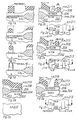
- Figures 1a-c illustrate a known method to create sublithographic polysilicon gate structures and includes minimal geometry patterning photoresist on a polysilicon layer (Figure 1a), isotropically etching the photoresist to reduce linewidth ( Figure 1b), and anisotropically etching the polysilicon with the reduced linewidth photoresist as etch mask ( Figure 1c).
- This approach has problems including contamination of the polysilicon.
- a photoresist mask for anisotropic etching polysilicon gates can leave residual ridges of hardened photoresist on the edges of the polysilicon gates after the etch.
- Plasma etch species harden the photoresist sidewalls during the polysilicon etch, and the subsequent oxygen plasma photoresist strip may not fully remove the ridges; Figure 1d.
- separate wet etches to strip the ridges may be used but lack robustness with respect to modifications. Any ridge residue will carbonize during later heat treatments and impede formation of titanium disilicide (TiSi 2 ) in a self-aligned gate silicidation process. Thus simple and complete removal of photoresist residue is a problem.
- EP-A-0 471 185 discloses TiN antireflective coating on titanium-coated polysilicon which, after photolithographic patterning has the titanium reacted with the polysilicon to form a titanium silicide.
- the present invention provides sublithographic patterns by use of an intermediate layer between photoresist and material to be etched together with lateral etching of the intermediate layer to shrink the linewidth.
- the intermediate layer acts as (1) an antireflective layer for photoresist exposure, (2) as a sacrifical layer for the subsequent lateral etch, and/or (3) a liftoff layer for removal of hardened photoresist residue.
- the present invention provides a method of lithography as mentioned in the beginning and comprising the features of the characterizing portion of the claim.
- Advantages of the invention include a simple method for sublithographic patterns and robust photoresist removal.
- the described methods of sublithographic pattern creation insert an intermediate layer between photoresist and the material to be patterned and use the following steps: first expose and develop a pattern in the photoresist with a minimal linewidth and then laterally (e.g., isotropically) remove photoresist or intermediate layer or both to uniformly shrink the intermediate layer to a subminimal linewidth which then provides the etch mask for the material to be patterned.
- the intermediate layer may provide (1) an anti-reflection function during photoresist exposure, (2) an etchstop or a sacrificial layer to protect the underlying material layer during the subsequent lateral removal, and/or (3) an etch residue liftoff layer after the material has been patterned.
- the sublithographic patterning and residue liftoff can be created over materials such as polysilicon, metal, insulator, ferroelectric, and so forth.
- the sublithographic pattern may define minimal sized items such as gate length and interconnection linewidth for integrated circuits.
- Figures 2a-h illustrate the first illustrative embodiment photoresist patterning method as could be used to form a mask for gate level polysilicon etching.
- monocrystalline silicon substrate 202 having (100) orientation and typically with both p and n type doped well regions for fabrication of devices plus also isolation oxides 203, gate oxide 204 with thickness typically 6-10 nm plus gate level polysilicon layer 206 with thickness typically 300-500 nm and either doped or undoped or doped only in certain portions. Then proceed with the following steps:
- the anisotropic etching of polysilicon 206 then proceeds with a helicon excited plasma from a gas mixture of Cl 2 , HBr, and He/O 2 (80%/20%) at a pressure of about 0.8 Pa (6 mTorr) and using the photoresist patterns 213-214 as etch mask.
- the Br provides sidewall passivation to insure anisotropy.
- Cl 2 /HBr/He-O 2 plasma may etch polysilicon about 300 times faster than oxide, and an overetch on oxide 204 will only remove a minimal amount of oxide; see Figure 3.
- a final oxygen plasma strips the photoresist plus a chlorine plasma or an SC1 rinse (NH 4 OH + H 2 O 2 + H 2 O solution) strips the TiN from the etched polysilicon without affecting either the polysilicon or the exposed gate oxide.
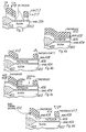
- Figures 4a-d illustrate the second illustrative embodiment photoresist patterning method as could also be used to form a mask for gate level polysilicon etching.
- monocrystalline silicon substrate 402 having (100) orientation with isolation oxides 403, gate oxide 404 with thickness 6 nm plus gate level polysilicon layer 406 with thickness 400 nm. Then proceed with the following steps:
- the etching of polysilicon 406 then proceeds with a plasma from a gas mixture of SF 6 plus HBr using the photoresist patterns 413-414 as etch mask.
- the Br provides sidewall passivation for anisotropy.
- the BARC etch of step (4) deposits material 450 on the BARC sidewall as illustrated in Figure 4d; and during the polysilicon etch this sidewall material migrates down the forming polysiicon sidewall as illustrated in Figure 6 and limits microtrenching at the sidewall base.
- Use a Cl 2 /HBr/He-O 2 plasma etch to finish and overetch because this mixture etches polysilicon about 300 times faster than oxide, and an overetch on oxide 404 will only remove a minimal amount of oxide.
- a final oxygen plasma strips the patterned photoresist plus BARC.
- the third illustrative embodiment again uses an isotropic etch to reduce the minimum linewidth of a photoresist mask with TiN antireflective coating in the case of a metal etch.
- aluminum interconnections often have TiN cladding to act as diffusion barriers and electromigration suppressors.
- Figure 7a shows silicon substrate 702 with insulated gate 704 and planarized oxide insulation 706 having a tungsten filled via 708 connecting down to the source/drain of the FET with gate 704 plus layer 712 of aluminum clad by layers 710 and 714 of TiN.
- top TiN cladding 714 acts as the anti-reflective coating.
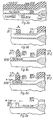
- Figures 8a-d illustrate the preferred embodiment method of the present invention as could be used to form a mask for gate level polysilicon etching.
- monocrystalline silicon substrate 802 having (100) orientation with isolation oxides 803, gate oxide 804 with thickness 6 nm plus gate level polysilicon layer 806 with thickness 400 nm. Then proceed with the following steps:
- Figures 9a-d illustrate a method as could be used with any of the foregoing embodiment linewidth reduction methods or could be used without them.
- the method uses the intermediate layer (possibly BARC) as a liftoff to remove the overlying photoresist or photoresist residue according to the following steps.
- Intermediate layer 917-918 may have been an organic BARC layer, and the method would follow the same steps with BARC dissolution by organic solvent providing the liftoff of the hardened sidewall portions 913-914.
- organic BARC sidewalls would likely also become hardened, so dissolution may require a particular solvent adapted to the type of BARC used.
- using an intermediate layer under photoresist for liftoff of hardened sidewalls also applies to etching metal levels, analogous to the third illustrative embodiment, and to etching vias through insulators.
- the preferred embodiment may be varied in many ways while retaining one or more of the features of use of an intermediate layer which may act as a buried anti-reflective coating, as a sacrificial layer for linewidth reduction, and as a liftoff for overlying photoresist or residue or other material.
- the isotropic etch to reduce photoresist linewidth could be somewhat anisotropic provided sufficient photoresist remains.
- the layer thicknesses and linewidths and etch chemistries and conditions could all be varied. Further, the preferred embodiment description all used I-line lithography, whereas with other exposure wavelengths using the same or different photoresist and anti-reflective coatings the same approach works. Further, variations could use a single wafer helicon plasma etcher or other types of plasma etchers including batch RIE, ECR RIE, and inductively coupled plasmas.
Landscapes
- Physics & Mathematics (AREA)
- General Physics & Mathematics (AREA)
- Engineering & Computer Science (AREA)
- Optics & Photonics (AREA)
- Structural Engineering (AREA)
- Architecture (AREA)
- Manufacturing & Machinery (AREA)
- Power Engineering (AREA)
- Microelectronics & Electronic Packaging (AREA)
- Computer Hardware Design (AREA)
- Condensed Matter Physics & Semiconductors (AREA)
- Drying Of Semiconductors (AREA)
- Internal Circuitry In Semiconductor Integrated Circuit Devices (AREA)
- Exposure Of Semiconductors, Excluding Electron Or Ion Beam Exposure (AREA)
- Exposure And Positioning Against Photoresist Photosensitive Materials (AREA)
- Photosensitive Polymer And Photoresist Processing (AREA)
- Weting (AREA)
Claims (1)
- Lithographieverfahren unter Verwendung einer Schicht eines strahlungsempfindlichen Materials (810) auf einer Antireflexions-Zwischenschicht (808), die sich auf einer zu strukturierenden ersten Schicht (806) befindet, wobei das Verfahren zunächst das strahlungsempfindliche Material (810) strukturiert, als nächstes die freigelegten Abschnitte der Antireflexions-Zwischenschicht (808) mit einem ersten anisotropen Ätzen entfernt und dann Abschnitte der ersten Schicht (806) unter Verwendung der strukturierten Antireflexions-Zwischenschicht (808) als eine Maske für ein zweites anisotropes Ätzen entfernt,
dadurch gekennzeichnet, daß
laterale Abschnitte der strukturierten Antireflexions-Zwischenschicht (821, 822) mit einem isotropen Ätzen entfernt werden, um eine verkleinerte strukturierte Antireflexions-Zwischenschicht (823, 824) zu bilden, so daß diese als die Maske für das Entfernen von Abschnitten der ersten Schicht (806) mit dem zweiten anisotropen Ätzen wirkt.
Applications Claiming Priority (2)
| Application Number | Priority Date | Filing Date | Title |
|---|---|---|---|
| US116695P | 1995-07-14 | 1995-07-14 | |
| US1166 | 1995-07-14 |
Publications (2)
| Publication Number | Publication Date |
|---|---|
| EP0753764A1 EP0753764A1 (de) | 1997-01-15 |
| EP0753764B1 true EP0753764B1 (de) | 2002-10-23 |
Family
ID=21694714
Family Applications (1)
| Application Number | Title | Priority Date | Filing Date |
|---|---|---|---|
| EP96111356A Expired - Lifetime EP0753764B1 (de) | 1995-07-14 | 1996-07-15 | Verbesserungen bei der Herstellung von Halbleitervorrichtungen |
Country Status (6)
| Country | Link |
|---|---|
| US (1) | US5976769A (de) |
| EP (1) | EP0753764B1 (de) |
| JP (1) | JPH09251988A (de) |
| KR (1) | KR100420910B1 (de) |
| DE (1) | DE69624413T2 (de) |
| TW (1) | TW332893B (de) |
Families Citing this family (49)
| Publication number | Priority date | Publication date | Assignee | Title |
|---|---|---|---|---|
| US6809421B1 (en) * | 1996-12-02 | 2004-10-26 | Kabushiki Kaisha Toshiba | Multichip semiconductor device, chip therefor and method of formation thereof |
| US5965461A (en) * | 1997-08-01 | 1999-10-12 | Advanced Micro Devices, Inc. | Controlled linewidth reduction during gate pattern formation using a spin-on barc |
| JP3165093B2 (ja) * | 1997-11-13 | 2001-05-14 | 松下電子工業株式会社 | 半導体装置およびその製造方法 |
| US6287975B1 (en) * | 1998-01-20 | 2001-09-11 | Tegal Corporation | Method for using a hard mask for critical dimension growth containment |
| US6221776B1 (en) * | 1998-05-05 | 2001-04-24 | Cypress Semiconductor Corp. | Anti-reflective coating used as a disposable etch stop |
| JP2000012687A (ja) * | 1998-06-23 | 2000-01-14 | Mitsubishi Electric Corp | 半導体装置及びその製造方法 |
| US6209193B1 (en) * | 1998-08-24 | 2001-04-03 | International Business Machines Corporation | Method of making read sensor with self-aligned low resistance leads |
| US6162587A (en) * | 1998-12-01 | 2000-12-19 | Advanced Micro Devices | Thin resist with transition metal hard mask for via etch application |
| US6362111B1 (en) * | 1998-12-09 | 2002-03-26 | Texas Instruments Incorporated | Tunable gate linewidth reduction process |
| JP2000208488A (ja) * | 1999-01-12 | 2000-07-28 | Kawasaki Steel Corp | エッチング方法 |
| JP2001015479A (ja) * | 1999-06-29 | 2001-01-19 | Toshiba Corp | 半導体装置の製造方法 |
| US6130155A (en) * | 1999-07-02 | 2000-10-10 | Promos Technologies, Inc. | Method of forming metal lines in an integrated circuit having reduced reaction with an anti-reflection coating |
| DE19937995C2 (de) * | 1999-08-11 | 2003-07-03 | Infineon Technologies Ag | Verfahren zur Strukturierung einer organischen Antireflexionsschicht |
| US6722376B2 (en) * | 1999-12-10 | 2004-04-20 | Micron Technology, Inc. | Polysilicon etch useful during the manufacture of a semiconductor device |
| US6365516B1 (en) | 2000-01-14 | 2002-04-02 | Advanced Micro Devices, Inc. | Advanced cobalt silicidation with in-situ hydrogen plasma clean |
| US6492275B2 (en) | 2000-01-21 | 2002-12-10 | Advanced Micro Devices, Inc. | Control of transistor performance through adjustment of spacer oxide profile with a wet etch |
| US20020086547A1 (en) * | 2000-02-17 | 2002-07-04 | Applied Materials, Inc. | Etch pattern definition using a CVD organic layer as an anti-reflection coating and hardmask |
| US6261936B1 (en) | 2000-06-07 | 2001-07-17 | Advanced Micro Devices, Inc. | Poly gate CD passivation for metrology control |
| US6283131B1 (en) * | 2000-09-25 | 2001-09-04 | Taiwan Semiconductor Manufacturing Company | In-situ strip process for polysilicon etching in deep sub-micron technology |
| US6482726B1 (en) * | 2000-10-17 | 2002-11-19 | Advanced Micro Devices, Inc. | Control trimming of hard mask for sub-100 nanometer transistor gate |
| US20020155389A1 (en) | 2000-10-24 | 2002-10-24 | Bharath Rangarajan | Inverse resist coating process |
| JP4530552B2 (ja) * | 2001-01-29 | 2010-08-25 | 富士通セミコンダクター株式会社 | 半導体装置及びその製造方法 |
| US20020187434A1 (en) * | 2001-05-25 | 2002-12-12 | Blatchford James W. | Process for device fabrication in which the size of lithographically produced features is subsequently reduced |
| EP1328013A1 (de) * | 2002-01-11 | 2003-07-16 | Infineon Technologies AG | Methode zur Erzeugung eines feinen Linienmusters auf einem Halbleiterwafer |
| US6774044B2 (en) * | 2002-01-14 | 2004-08-10 | Taiwan Semiconductor Manufacturing Co., Ltd | Reducing photoresist shrinkage via plasma treatment |
| FR2840453B1 (fr) * | 2002-06-04 | 2005-06-24 | St Microelectronics Sa | Procede de fabrication d'un transistor mos de longueur de grille reduite, et circuit integre comportant un tel transistor |
| US6923920B2 (en) * | 2002-08-14 | 2005-08-02 | Lam Research Corporation | Method and compositions for hardening photoresist in etching processes |
| US6991893B2 (en) * | 2002-10-31 | 2006-01-31 | Intel Corporation | Controlling resist profiles through substrate modification |
| JP2004172311A (ja) * | 2002-11-19 | 2004-06-17 | Renesas Technology Corp | 半導体装置の製造方法 |
| KR20040061616A (ko) * | 2002-12-31 | 2004-07-07 | 동부전자 주식회사 | 비휘발성 메모리 장치의 제조 방법 |
| US7262070B2 (en) * | 2003-09-29 | 2007-08-28 | Intel Corporation | Method to make a weight compensating/tuning layer on a substrate |
| US20060096081A1 (en) * | 2004-06-30 | 2006-05-11 | Hitachi Global Storage Technologies | Methods of making magnetic write heads with use of a resist channel shrinking solution having corrosion inhibitors |
| US7343666B2 (en) | 2004-06-30 | 2008-03-18 | Hitachi Global Storage Technologies Netherlands B.V. | Methods of making magnetic write heads with use of linewidth shrinkage techniques |
| US20060169968A1 (en) * | 2005-02-01 | 2006-08-03 | Thomas Happ | Pillar phase change memory cell |
| US7517796B2 (en) * | 2005-02-17 | 2009-04-14 | Sandisk 3D Llc | Method for patterning submicron pillars |
| JP2007035939A (ja) * | 2005-07-27 | 2007-02-08 | Oki Electric Ind Co Ltd | 半導体装置の製造方法 |
| KR100685903B1 (ko) * | 2005-08-31 | 2007-02-26 | 동부일렉트로닉스 주식회사 | 반도체 소자의 제조 방법 |
| KR100720481B1 (ko) * | 2005-11-28 | 2007-05-22 | 동부일렉트로닉스 주식회사 | 반도체 소자의 제조 방법 |
| TW200741959A (en) * | 2006-04-20 | 2007-11-01 | Min-Chang Dong | A die and method fabricating the same |
| US8039309B2 (en) * | 2007-05-10 | 2011-10-18 | Texas Instruments Incorporated | Systems and methods for post-circuitization assembly |
| KR101025741B1 (ko) * | 2008-09-02 | 2011-04-04 | 주식회사 하이닉스반도체 | 수직 채널 트랜지스터의 활성필라 제조방법 |
| JP5203340B2 (ja) * | 2009-12-01 | 2013-06-05 | 東京エレクトロン株式会社 | 半導体装置の製造方法 |
| US8980753B2 (en) * | 2010-09-21 | 2015-03-17 | United Mircroelectronics Corp. | Metal gate transistor and method for fabricating the same |
| US9070851B2 (en) | 2010-09-24 | 2015-06-30 | Seoul Semiconductor Co., Ltd. | Wafer-level light emitting diode package and method of fabricating the same |
| JP5682290B2 (ja) * | 2010-12-20 | 2015-03-11 | 東京エレクトロン株式会社 | 炭素含有薄膜のスリミング方法及び酸化装置 |
| CN103681234B (zh) * | 2012-09-10 | 2016-03-16 | 中芯国际集成电路制造(上海)有限公司 | 自对准双重图形的形成方法 |
| CN103681293B (zh) * | 2012-09-10 | 2016-04-20 | 中芯国际集成电路制造(上海)有限公司 | 自对准双重图形化方法 |
| US20150368557A1 (en) * | 2014-06-23 | 2015-12-24 | Hyosan Lee | Metal etchant compositions and methods of fabricating a semiconductor device using the same |
| CN205944139U (zh) | 2016-03-30 | 2017-02-08 | 首尔伟傲世有限公司 | 紫外线发光二极管封装件以及包含此的发光二极管模块 |
Family Cites Families (6)
| Publication number | Priority date | Publication date | Assignee | Title |
|---|---|---|---|---|
| US4820611A (en) * | 1987-04-24 | 1989-04-11 | Advanced Micro Devices, Inc. | Titanium nitride as an antireflection coating on highly reflective layers for photolithography |
| US5106786A (en) * | 1989-10-23 | 1992-04-21 | At&T Bell Laboratories | Thin coatings for use in semiconductor integrated circuits and processes as antireflection coatings consisting of tungsten silicide |
| US5126289A (en) * | 1990-07-20 | 1992-06-30 | At&T Bell Laboratories | Semiconductor lithography methods using an arc of organic material |
| US5034348A (en) * | 1990-08-16 | 1991-07-23 | International Business Machines Corp. | Process for forming refractory metal silicide layers of different thicknesses in an integrated circuit |
| US5439847A (en) * | 1993-11-05 | 1995-08-08 | At&T Corp. | Integrated circuit fabrication with a raised feature as mask |
| US5525542A (en) * | 1995-02-24 | 1996-06-11 | Motorola, Inc. | Method for making a semiconductor device having anti-reflective coating |
-
1996
- 1996-07-12 US US08/680,340 patent/US5976769A/en not_active Expired - Lifetime
- 1996-07-13 KR KR1019960028361A patent/KR100420910B1/ko not_active Expired - Fee Related
- 1996-07-15 DE DE69624413T patent/DE69624413T2/de not_active Expired - Lifetime
- 1996-07-15 EP EP96111356A patent/EP0753764B1/de not_active Expired - Lifetime
- 1996-07-15 JP JP8185162A patent/JPH09251988A/ja active Pending
- 1996-10-08 TW TW085112259A patent/TW332893B/zh not_active IP Right Cessation
Also Published As
| Publication number | Publication date |
|---|---|
| DE69624413T2 (de) | 2003-06-18 |
| DE69624413D1 (de) | 2002-11-28 |
| TW332893B (en) | 1998-06-01 |
| JPH09251988A (ja) | 1997-09-22 |
| KR100420910B1 (ko) | 2004-05-17 |
| EP0753764A1 (de) | 1997-01-15 |
| US5976769A (en) | 1999-11-02 |
| KR970008324A (ko) | 1997-02-24 |
Similar Documents
| Publication | Publication Date | Title |
|---|---|---|
| EP0753764B1 (de) | Verbesserungen bei der Herstellung von Halbleitervorrichtungen | |
| US5804088A (en) | Intermediate layer lithography | |
| EP0753885B1 (de) | Verbesserungen in Verfahren zur Herstellung von Halbleitervorrichtungen | |
| US6362111B1 (en) | Tunable gate linewidth reduction process | |
| US5910453A (en) | Deep UV anti-reflection coating etch | |
| US20060205223A1 (en) | Line edge roughness reduction compatible with trimming | |
| US4758305A (en) | Contact etch method | |
| US6423475B1 (en) | Sidewall formation for sidewall patterning of sub 100 nm structures | |
| JPH07307263A (ja) | 集積回路基板の上に位置するパターン化層を形成する方法 | |
| JPH11186235A (ja) | 半導体装置の製造方法 | |
| WO1997043782A1 (en) | Method of patterning a substrate using spin-on glass as a hard mask | |
| US6900139B1 (en) | Method for photoresist trim endpoint detection | |
| US5968711A (en) | Method of dry etching A1Cu using SiN hard mask | |
| US6211557B1 (en) | Contact structure using taper contact etching and polycide step | |
| JPH0845906A (ja) | パターン形成方法及び該パターン形成方法を用いた半導体装置の製造方法 | |
| EP0753763A1 (de) | Verbesserungen bezüglich Halbleitervorrichtungen | |
| KR100551071B1 (ko) | 반도체소자 제조방법 | |
| US20070161255A1 (en) | Method for etching with hardmask | |
| KR100939109B1 (ko) | 반도체소자 제조방법 | |
| KR100281275B1 (ko) | 반도체 소자의 다결정 실리콘 배선 제조방법 | |
| JPH08153704A (ja) | 半導体装置の製造方法 | |
| JP3450253B2 (ja) | 半導体装置の製造方法 | |
| US6451706B1 (en) | Attenuation of reflecting lights by surface treatment | |
| KR20030058247A (ko) | 패턴 변형을 방지할 수 있는 반도체 소자 제조 방법 | |
| Marriott et al. | A Method For Generating Sloped Contact Holes Using A Cantilever Resist Structure |
Legal Events
| Date | Code | Title | Description |
|---|---|---|---|
| PUAI | Public reference made under article 153(3) epc to a published international application that has entered the european phase |
Free format text: ORIGINAL CODE: 0009012 |
|
| AK | Designated contracting states |
Kind code of ref document: A1 Designated state(s): DE FR GB IT NL |
|
| 17P | Request for examination filed |
Effective date: 19970702 |
|
| 17Q | First examination report despatched |
Effective date: 19990125 |
|
| RIC1 | Information provided on ipc code assigned before grant |
Free format text: 7H 01L 21/027 A, 7G 02B 1/11 B, 7H 01L 21/268 B |
|
| RTI1 | Title (correction) |
Free format text: IMPROVEMENTS IN OR RELATING TO THE FABRICATION OF SEMICONDUCTOR DEVICES |
|
| GRAG | Despatch of communication of intention to grant |
Free format text: ORIGINAL CODE: EPIDOS AGRA |
|
| GRAG | Despatch of communication of intention to grant |
Free format text: ORIGINAL CODE: EPIDOS AGRA |
|
| GRAH | Despatch of communication of intention to grant a patent |
Free format text: ORIGINAL CODE: EPIDOS IGRA |
|
| GRAH | Despatch of communication of intention to grant a patent |
Free format text: ORIGINAL CODE: EPIDOS IGRA |
|
| GRAA | (expected) grant |
Free format text: ORIGINAL CODE: 0009210 |
|
| AK | Designated contracting states |
Kind code of ref document: B1 Designated state(s): DE FR GB IT NL |
|
| PG25 | Lapsed in a contracting state [announced via postgrant information from national office to epo] |
Ref country code: NL Free format text: LAPSE BECAUSE OF FAILURE TO SUBMIT A TRANSLATION OF THE DESCRIPTION OR TO PAY THE FEE WITHIN THE PRESCRIBED TIME-LIMIT Effective date: 20021023 Ref country code: IT Free format text: LAPSE BECAUSE OF FAILURE TO SUBMIT A TRANSLATION OF THE DESCRIPTION OR TO PAY THE FEE WITHIN THE PRESCRIBED TIME-LIMIT;WARNING: LAPSES OF ITALIAN PATENTS WITH EFFECTIVE DATE BEFORE 2007 MAY HAVE OCCURRED AT ANY TIME BEFORE 2007. THE CORRECT EFFECTIVE DATE MAY BE DIFFERENT FROM THE ONE RECORDED. Effective date: 20021023 |
|
| REG | Reference to a national code |
Ref country code: GB Ref legal event code: FG4D |
|
| REF | Corresponds to: |
Ref document number: 69624413 Country of ref document: DE Date of ref document: 20021128 |
|
| NLV1 | Nl: lapsed or annulled due to failure to fulfill the requirements of art. 29p and 29m of the patents act | ||
| ET | Fr: translation filed | ||
| PLBE | No opposition filed within time limit |
Free format text: ORIGINAL CODE: 0009261 |
|
| STAA | Information on the status of an ep patent application or granted ep patent |
Free format text: STATUS: NO OPPOSITION FILED WITHIN TIME LIMIT |
|
| 26N | No opposition filed |
Effective date: 20030724 |
|
| PGFP | Annual fee paid to national office [announced via postgrant information from national office to epo] |
Ref country code: GB Payment date: 20110622 Year of fee payment: 16 |
|
| PGFP | Annual fee paid to national office [announced via postgrant information from national office to epo] |
Ref country code: FR Payment date: 20110727 Year of fee payment: 16 |
|
| PGFP | Annual fee paid to national office [announced via postgrant information from national office to epo] |
Ref country code: DE Payment date: 20110729 Year of fee payment: 16 |
|
| GBPC | Gb: european patent ceased through non-payment of renewal fee |
Effective date: 20120715 |
|
| REG | Reference to a national code |
Ref country code: FR Ref legal event code: ST Effective date: 20130329 |
|
| PG25 | Lapsed in a contracting state [announced via postgrant information from national office to epo] |
Ref country code: FR Free format text: LAPSE BECAUSE OF NON-PAYMENT OF DUE FEES Effective date: 20120731 Ref country code: DE Free format text: LAPSE BECAUSE OF NON-PAYMENT OF DUE FEES Effective date: 20130201 Ref country code: GB Free format text: LAPSE BECAUSE OF NON-PAYMENT OF DUE FEES Effective date: 20120715 |
|
| REG | Reference to a national code |
Ref country code: DE Ref legal event code: R119 Ref document number: 69624413 Country of ref document: DE Effective date: 20130201 |