EP0750688B1 - Batchladesystem für cvd - Google Patents
Batchladesystem für cvd Download PDFInfo
- Publication number
- EP0750688B1 EP0750688B1 EP95913951A EP95913951A EP0750688B1 EP 0750688 B1 EP0750688 B1 EP 0750688B1 EP 95913951 A EP95913951 A EP 95913951A EP 95913951 A EP95913951 A EP 95913951A EP 0750688 B1 EP0750688 B1 EP 0750688B1
- Authority
- EP
- European Patent Office
- Prior art keywords
- inserts
- carrier
- insert
- peg
- cvd
- Prior art date
- Legal status (The legal status is an assumption and is not a legal conclusion. Google has not performed a legal analysis and makes no representation as to the accuracy of the status listed.)
- Expired - Lifetime
Links
- 238000011068 loading method Methods 0.000 title abstract description 18
- 238000000576 coating method Methods 0.000 claims abstract description 22
- 238000000034 method Methods 0.000 claims abstract description 22
- 239000011248 coating agent Substances 0.000 claims abstract description 17
- 238000005229 chemical vapour deposition Methods 0.000 claims abstract description 11
- 238000005520 cutting process Methods 0.000 claims abstract description 8
- 230000000284 resting effect Effects 0.000 claims abstract description 3
- 229910052751 metal Inorganic materials 0.000 claims description 6
- 239000002184 metal Substances 0.000 claims description 6
- OKTJSMMVPCPJKN-UHFFFAOYSA-N Carbon Chemical compound [C] OKTJSMMVPCPJKN-UHFFFAOYSA-N 0.000 claims description 3
- 229910002804 graphite Inorganic materials 0.000 claims description 3
- 239000010439 graphite Substances 0.000 claims description 3
- 239000011819 refractory material Substances 0.000 claims description 3
- ZOKXTWBITQBERF-UHFFFAOYSA-N Molybdenum Chemical compound [Mo] ZOKXTWBITQBERF-UHFFFAOYSA-N 0.000 claims description 2
- 239000000919 ceramic Substances 0.000 claims description 2
- 229910052750 molybdenum Inorganic materials 0.000 claims description 2
- 239000011733 molybdenum Substances 0.000 claims description 2
- 238000004519 manufacturing process Methods 0.000 abstract description 3
- 239000007789 gas Substances 0.000 description 9
- 125000006850 spacer group Chemical group 0.000 description 3
- 238000000151 deposition Methods 0.000 description 2
- 230000008021 deposition Effects 0.000 description 2
- 229910000640 Fe alloy Inorganic materials 0.000 description 1
- 239000000969 carrier Substances 0.000 description 1
- 239000002537 cosmetic Substances 0.000 description 1
- 238000002845 discoloration Methods 0.000 description 1
- 238000009826 distribution Methods 0.000 description 1
- 230000001788 irregular Effects 0.000 description 1
- 238000012856 packing Methods 0.000 description 1
- 238000005268 plasma chemical vapour deposition Methods 0.000 description 1
Images


Classifications
-
- C—CHEMISTRY; METALLURGY
- C23—COATING METALLIC MATERIAL; COATING MATERIAL WITH METALLIC MATERIAL; CHEMICAL SURFACE TREATMENT; DIFFUSION TREATMENT OF METALLIC MATERIAL; COATING BY VACUUM EVAPORATION, BY SPUTTERING, BY ION IMPLANTATION OR BY CHEMICAL VAPOUR DEPOSITION, IN GENERAL; INHIBITING CORROSION OF METALLIC MATERIAL OR INCRUSTATION IN GENERAL
- C23C—COATING METALLIC MATERIAL; COATING MATERIAL WITH METALLIC MATERIAL; SURFACE TREATMENT OF METALLIC MATERIAL BY DIFFUSION INTO THE SURFACE, BY CHEMICAL CONVERSION OR SUBSTITUTION; COATING BY VACUUM EVAPORATION, BY SPUTTERING, BY ION IMPLANTATION OR BY CHEMICAL VAPOUR DEPOSITION, IN GENERAL
- C23C16/00—Chemical coating by decomposition of gaseous compounds, without leaving reaction products of surface material in the coating, i.e. chemical vapour deposition [CVD] processes
- C23C16/44—Chemical coating by decomposition of gaseous compounds, without leaving reaction products of surface material in the coating, i.e. chemical vapour deposition [CVD] processes characterised by the method of coating
- C23C16/458—Chemical coating by decomposition of gaseous compounds, without leaving reaction products of surface material in the coating, i.e. chemical vapour deposition [CVD] processes characterised by the method of coating characterised by the method used for supporting substrates in the reaction chamber
Definitions
- the present invention relates to a CVD-batch loading method used in connection with coating of cutting inserts suitable for a rational production in larger scale allowing fully automatic CVD loading.
- CVD-batches are generally used. Rational loading and unloading of the inserts from the CVD-reactor is thus required. Transportation of the whole load or parts of the loads must be possible to be carried out safely particularly prior to the coating operation.
- Another problem related to mass volume CVD is to find an appropriate loading arrangement of the inserts that will allow a well controlled gas flow through the CVD-reactor in order to ensure high and even coating quality throughout the whole load.
- the inserts are allowed to hang in slits in a tray.
- This method has the disadvantage of leaving contact marks on the clearance faces of the inserts.
- the system is unstable and there is always a potential risk during transportation that the inserts fall over and completely rearrange the packing.
- all surfaces of an insert with this type of loading will not be exposed to the same amount of gas flow during the coating process. This may result in serious variation in the coating thickness and hence the quality of the coating.
- the inserts are placed on woven metal nets.
- the load is built up by piling each metal net on top of each other.
- the inserts are threaded up on a rod. Spacers between each insert are generally used to avoid contact between the inserts.
- the rods may be oriented horizontally or vertically in the CVD-reactor.
- the main drawbacks of this method are the very complicated and time consuming loading and unloading procedure. Contact marks between the spacer and the inserts are difficult to avoid.
- This method can be applied to inserts having a central hole for clamping.
- German patent DE 39 02 532 a loading system is disclosed in which the inserts are stacked on top of each other on a central pin possibly with a spacer between. As a result the inserts will be only partially coated. This method is aimed for plasma CVD and will not be fully applicable to ordinary CVD since the inserts will be "glued" or grown together during an ordinary CVD-process.
- JP-A-63 033 571 and EP-A-0 551 737 disclose CVD-methods for providing uniform coatings over the outer surfaces of articles. The articles rest on supports at only a few points.
- the object of the present invention is to eliminate most of problems associated with the prior art loading systems.
- the batch loading system according to the present invention consist of a peg attached to a carrier.
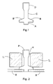
- Fig 1 shows an example of a peg according to the present invention in side view.
- the peg comprises a foot A and shoulders B and a neck C and a head D.
- the shoulders B have a cicular as well as non-circular cross-section such as square, triangular or rectangular but can also be in the form of wings.
- the foot A is preferably circular.
- Figs 2 - 7 show various embodiments of the present invention.
- P is peg, X carrier, I 1 insert 1, I 2 insert 2, I 3 insert 3, I 4 insert 4 and F depression.
- inserts with a central hole for clamping which generally is the case for inserts used for turning, is positioned on a peg P as shown in Fig 2.
- the insert rests on the peg shoulder B having such a shape that there is minimal contact between the peg and the insert and preferably so that contact occurs at only a few tiny points. This can be done by altering the shape of the shoulder (e.g. circular, rectangular, square or in the from of wings) depending upon the shape of the hole or the insert itself.
- Inside the hole H there is a wide passage around the neck to ensure even coating thickness of the inner walls of the hole.
- the dimension of the hole H is important for a safe fixturing of the insert into its tool holder.
- the function of the head D which protrudes above the top surface of the insert I 1 , is to serve as a support for the next carrier placed on top.
- the thicker head acts to prevent the inserts from tilting from their horizontal position and touch the upper and/or the lower carrier surfaces.
- the hole is wider on the top surface of the insert and then a peg without a head can be used.
- the peg P is attached to the carrier X.
- a loading arrangement according to the invention is illustrated in Fig 3 for square inserts in which the pegs are placed between the inserts and generally supports at least two inserts.
- the peg shoulder shall have such a shape e.g. a sharp edge or tip that the contact area is minimised.
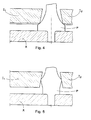
- a peg similar to Fig 1 is used as shown in Fig 4 in which the peg supports an insert only at the middle of the edge. This arrangement is preferably used for single sided inserts.
- a peg as shown in Fig 5 is used.
- the peg supports an insert essentially in the middle of each clearance face.
- a peg as shown in Fig 6 is used.
- the peg supports essentially in the bottom of the chipbreaker which has to deep enough so as to ensure maximum stability of the loading arrangement.
- plane inserts are provided with a depression between the corners to receive the shoulders of the pegs.
- the pegs serve also as support for a following carrier.
- the neck C and head D can be excluded.
- an alternative embodiment according to Fig 7 can be used.
- inserts are provided with a central hole (not shown) or depression F of a suitable depth and shape adapted to the peg.
- Pegs according to the invention are made of a refractory material such as ceramics, reinforced graphite, molybdenum preferably cemented carbide.
- the carrier may be a woven metal net of e.g. an iron alloy with a suitable mesh size or a tray of graphite or other refractory material with mounting holes drilled for the pegs.
- the peg foot is snapped into the metal net or pressed into the mounting holes in the tray.
- a desired number of pegs is mounted in each carrier in a regular pattern.
- the distance between the pegs as well as the height of the pegs is selected to give a desired free gas volume around each insert.
- a free volume around each insert of 1 - 5 mm is generally suitable.
- the carriers are piled on top of each other (preferably resting on the peg heads) to complete a full CVD load.
- holes are suitably drilled in the trays in the areas between the pegs.
- the size and positioning of these holes can be optimized so that the gas flow can be controlled and directed in almost any desired way through the pile of trays.
- the holes in the trays can optionally be omitted.
- the loading system of the presently claimed invention allows the process gases to reach all essential surfaces of the inserts improving the coating thickness distribution, minimising discoloration due to irregular gas flow pattern and reducing coating time.
- the rigid and exact positioning of the inserts allows a safe transportation prior to and after the coating step and also an automatic loading system. By using a suitable cross-section of the shoulders, the only contact between the peg and the insert will occur at only a few, less than five, tiny points which are not critical for the performance of the coated inserts.
Landscapes
- Chemical & Material Sciences (AREA)
- General Chemical & Material Sciences (AREA)
- Chemical Kinetics & Catalysis (AREA)
- Engineering & Computer Science (AREA)
- Materials Engineering (AREA)
- Mechanical Engineering (AREA)
- Metallurgy (AREA)
- Organic Chemistry (AREA)
- Chemical Vapour Deposition (AREA)
- Cutting Tools, Boring Holders, And Turrets (AREA)
- Physical Or Chemical Processes And Apparatus (AREA)
- Turning (AREA)
Claims (13)
- Verfahren zum Beschichten von Schneidwerkzeugeinsätzen durch CVD-Methoden mit einem vollständig bedeckenden Überzug, während welcher Beschichtungsstufe die Einsätze auf einer Unterstützung ruhen, dadurch gekennzeichnet, daß diese Unterstützung ein an einem Träger befestigter Stift ist, wobei dieser Stift einen Fuß A und Schultern B umfaßt und der Fuß des Stiftes an dem Träger befestigt oder in den Träger eingerastet ist.
- Verfahren nach dem vorausgehenden Anspruch, dadurch gekennzeichnet, daß der Stift weiterhin einen Hals C und einen Kopf D umfaßt, der als Unterstützung für einen anderen über diesem Träger angeordneten Träger dient.
- Verfahren nach einem der vorausgehenden Ansprüche, dadurch gekennzeichnet, daß der Stift durch ein Loch in einem Einsatz geht, wobei der Einsatz auf dem Schulterabschnitt ruht.
- Verfahren nach einem der Ansprüche 1 und 2, dadurch gekennzeichnet, daß die Stifte zwischen den Einsätzen angeordnet sind.
- Verfahren nach Anspruch 4, dadurch gekennzeichnet, daß der Einsatz auf den Schultern mit dem Boden eines Spanbrechers ruht.
- Verfahren nach Anspruch 4, dadurch gekennzeichnet, daß der Einsatz auf den Schultern im wesentlichen in der Mitte einer Freifläche ruht.
- Verfahren nach Anspruch 4, dadurch gekennzeichnet, daß der Einsatz auf den Schultern in der Mitte einer Kante ruht.
- Träger zum Tragen von Schneidwerkzeugeinsätzen, wenn diese mit einem CVD-Chargenbeschichtungsverfahren nach einem der Ansprüche 1 bis 7 beschichtet werden, wobei der Träger einen Boden (X) aus einem hitzebeständigen Material oder ein Metallnetz (X) umfaßt, dadurch gekennzeichnet, daß Stifte (P) an dem Boden oder Netz befestigt sind, daß jeder dieser Stifte einen Fuß (A) und eine Schulter (B) umfaßt und daß die Schneideinsätze auf diesen Schultern ruhen.
- Träger nach Anspruch 8, dadurch gekennzeichnet, daß jeder Stift weiterhin einen Hals (C) und einen Kopf (D) umfaßt, wobei mehrere dieser Köpfe als eine Unterstützung für einen anderen Träger dienen, der über diesem Träger angeordnet ist.
- Träger nach Anspruch 8 oder 9, dadurch gekennzeichnet, daß der Boden aus Keramik, verstärktem Graphit, Molybdän oder Sintercarbid besteht.
- Schneideinsatz, der nach einem CVD-Verfahren nach Anspruch 1 beschichtet ist, mit einer oberen Oberfläche, einer ebenen Bodenfläche und Freiflächen, dadurch gekennzeichnet, daß ein oder mehrere Vertiefungen in der ebenen Bodenfläche vorgesehen sind, wobei jede dieser Vertiefungen so ausgebildet ist, daß sie einen Stift aufnehmen kann.
- Einsatz nach Anspruch 11, dadurch gekennzeichnet, daß eine Vertiefung zwischen benachbarten Ecken angeordnet ist.
- Einsatz nach Anspruch 11, dadurch gekennzeichnet, daß eine Vertiefung (F) mittig angeordnet ist.
Applications Claiming Priority (3)
| Application Number | Priority Date | Filing Date | Title |
|---|---|---|---|
| SE9400950 | 1994-03-18 | ||
| SE9400950A SE509984C2 (sv) | 1994-03-18 | 1994-03-18 | Chargeringssystem för CVD |
| PCT/SE1995/000276 WO1995025829A1 (en) | 1994-03-18 | 1995-03-17 | Batch loading system for cvd |
Publications (2)
| Publication Number | Publication Date |
|---|---|
| EP0750688A1 EP0750688A1 (de) | 1997-01-02 |
| EP0750688B1 true EP0750688B1 (de) | 1998-08-12 |
Family
ID=20393359
Family Applications (1)
| Application Number | Title | Priority Date | Filing Date |
|---|---|---|---|
| EP95913951A Expired - Lifetime EP0750688B1 (de) | 1994-03-18 | 1995-03-17 | Batchladesystem für cvd |
Country Status (8)
| Country | Link |
|---|---|
| US (2) | US5576058A (de) |
| EP (1) | EP0750688B1 (de) |
| JP (1) | JP3742831B2 (de) |
| AT (1) | ATE169692T1 (de) |
| DE (1) | DE69504045T2 (de) |
| IL (1) | IL113015A (de) |
| SE (1) | SE509984C2 (de) |
| WO (1) | WO1995025829A1 (de) |
Cited By (1)
| Publication number | Priority date | Publication date | Assignee | Title |
|---|---|---|---|---|
| CN103726031A (zh) * | 2013-12-24 | 2014-04-16 | 成都工具研究所有限公司 | 化学气相沉积设备的工件装卡工具 |
Families Citing this family (19)
| Publication number | Priority date | Publication date | Assignee | Title |
|---|---|---|---|---|
| SE509984C2 (sv) * | 1994-03-18 | 1999-03-29 | Sandvik Ab | Chargeringssystem för CVD |
| EP0992605A3 (de) * | 1998-10-02 | 2002-11-13 | Sumitomo Special Metals Co., Ltd. | Tragelement, Haltevorrichtung, Prozess und Apparat im Anwendungsbereich der Oberflächenbehandlung |
| SE514666C2 (sv) | 1999-07-05 | 2001-04-02 | Sandvik Ab | Metod för fixering av skär vid PVD-beläggning |
| FR2819047B1 (fr) * | 2000-12-28 | 2003-06-27 | Snecma Moteurs | Support approprie pour le traitement thermique d'une piece metallique et procede de traitement thermique |
| SE527351C2 (sv) * | 2003-07-10 | 2006-02-14 | Seco Tools Ab | Metod att belägga skär |
| JP2007518878A (ja) * | 2003-12-22 | 2007-07-12 | セコ ツールズ アクティエボラーグ | 切削工具を被覆するための支持物体とその方法 |
| WO2006076924A1 (en) * | 2005-01-24 | 2006-07-27 | Danfoss A/S | A method for coating an object |
| US7662437B2 (en) * | 2005-03-24 | 2010-02-16 | Honeywell International Inc. | Template for arranging spacers on a preform and method of densifying a preform including the use of spacers positioned by a template |
| US7874770B2 (en) † | 2005-03-30 | 2011-01-25 | Sumitomo Electric Hardmetal Corp. | Indexable insert |
| JP4931507B2 (ja) * | 2005-07-26 | 2012-05-16 | スネクマ | 壁内に形成された冷却流路 |
| CN102534565B (zh) * | 2012-03-22 | 2013-07-03 | 株洲欧科亿硬质合金有限公司 | 一种涂层刀片生产用装载舟皿及其应用 |
| JP6337107B2 (ja) * | 2014-05-28 | 2018-06-06 | 京セラ株式会社 | 切削インサートの製造方法 |
| DE102016211775A1 (de) * | 2016-06-29 | 2018-01-04 | Schunk Kohlenstofftechnik Gmbh | Werkstückträger und Verfahren zur Herstellung eines Werkstückträgers |
| KR102040378B1 (ko) * | 2016-12-20 | 2019-11-05 | 주식회사 티씨케이 | 지그를 이용한 반도체 제조용 부품의 제조방법 및 제조장치 |
| WO2018117558A1 (ko) * | 2016-12-20 | 2018-06-28 | 주식회사 티씨케이 | 지그를 이용한 반도체 제조용 부품의 제조방법 및 제조장치 |
| WO2018117559A1 (ko) * | 2016-12-20 | 2018-06-28 | 주식회사 티씨케이 | Sic 증착층을 포함하는 반도체 제조용 부품 및 그 제조방법 |
| KR102051668B1 (ko) * | 2016-12-20 | 2019-12-04 | 주식회사 티씨케이 | SiC 증착층을 포함하는 반도체 제조용 부품 및 그 제조방법 |
| US20200255941A1 (en) * | 2019-02-11 | 2020-08-13 | Kennametal Inc. | Supports for chemical vapor deposition coating applications |
| KR102642090B1 (ko) * | 2021-08-24 | 2024-02-29 | 주식회사 케이엔제이 | 지지 소켓 및 증착층을 포함하는 부품 제조 방법 |
Citations (1)
| Publication number | Priority date | Publication date | Assignee | Title |
|---|---|---|---|---|
| JPS6333571A (ja) * | 1986-07-25 | 1988-02-13 | Nippon Telegr & Teleph Corp <Ntt> | 球状物の成膜方法 |
Family Cites Families (9)
| Publication number | Priority date | Publication date | Assignee | Title |
|---|---|---|---|---|
| US3496010A (en) * | 1966-10-05 | 1970-02-17 | Texas Instruments Inc | Machining silicon coating prior to vapor deposition of silicon carbide |
| US3964937A (en) * | 1973-08-13 | 1976-06-22 | Materials Technology Corporation | Method of making a composite coating |
| US4558388A (en) * | 1983-11-02 | 1985-12-10 | Varian Associates, Inc. | Substrate and substrate holder |
| DE3902532C1 (de) * | 1989-01-28 | 1989-11-23 | Krupp Widia Gmbh, 4300 Essen, De | |
| EP0458342A1 (de) * | 1990-05-25 | 1991-11-27 | Idemitsu Petrochemical Company Limited | Verfahren zur Herstellung von einem diamantfilmbeschichteten Werkstoff |
| US5393349A (en) * | 1991-08-16 | 1995-02-28 | Tokyo Electron Sagami Kabushiki Kaisha | Semiconductor wafer processing apparatus |
| JP2513976B2 (ja) * | 1991-12-13 | 1996-07-10 | エイ・ティ・アンド・ティ・コーポレーション | 複数の球状部品の被覆方法 |
| SE509984C2 (sv) * | 1994-03-18 | 1999-03-29 | Sandvik Ab | Chargeringssystem för CVD |
| US5543022A (en) * | 1995-01-17 | 1996-08-06 | Hmt Technology Corporation | Disc-handling apparatus |
-
1994
- 1994-03-18 SE SE9400950A patent/SE509984C2/xx not_active IP Right Cessation
-
1995
- 1995-03-16 IL IL11301595A patent/IL113015A/en not_active IP Right Cessation
- 1995-03-17 US US08/405,782 patent/US5576058A/en not_active Expired - Lifetime
- 1995-03-17 EP EP95913951A patent/EP0750688B1/de not_active Expired - Lifetime
- 1995-03-17 JP JP52457995A patent/JP3742831B2/ja not_active Expired - Lifetime
- 1995-03-17 DE DE69504045T patent/DE69504045T2/de not_active Expired - Lifetime
- 1995-03-17 AT AT95913951T patent/ATE169692T1/de active
- 1995-03-17 WO PCT/SE1995/000276 patent/WO1995025829A1/en not_active Ceased
-
1996
- 1996-08-28 US US08/703,966 patent/US5759621A/en not_active Expired - Lifetime
Patent Citations (1)
| Publication number | Priority date | Publication date | Assignee | Title |
|---|---|---|---|---|
| JPS6333571A (ja) * | 1986-07-25 | 1988-02-13 | Nippon Telegr & Teleph Corp <Ntt> | 球状物の成膜方法 |
Cited By (1)
| Publication number | Priority date | Publication date | Assignee | Title |
|---|---|---|---|---|
| CN103726031A (zh) * | 2013-12-24 | 2014-04-16 | 成都工具研究所有限公司 | 化学气相沉积设备的工件装卡工具 |
Also Published As
| Publication number | Publication date |
|---|---|
| IL113015A (en) | 1998-08-16 |
| JP3742831B2 (ja) | 2006-02-08 |
| DE69504045D1 (de) | 1998-09-17 |
| IL113015A0 (en) | 1995-06-29 |
| ATE169692T1 (de) | 1998-08-15 |
| US5576058A (en) | 1996-11-19 |
| DE69504045T2 (de) | 1998-12-10 |
| US5759621A (en) | 1998-06-02 |
| WO1995025829A1 (en) | 1995-09-28 |
| JPH09510507A (ja) | 1997-10-21 |
| SE509984C2 (sv) | 1999-03-29 |
| SE9400950D0 (sv) | 1994-03-18 |
| SE9400950L (sv) | 1995-09-19 |
| EP0750688A1 (de) | 1997-01-02 |
Similar Documents
| Publication | Publication Date | Title |
|---|---|---|
| EP0750688B1 (de) | Batchladesystem für cvd | |
| US20050132957A1 (en) | Carrier body and method | |
| US5858103A (en) | Vertical wafer boat | |
| US5518549A (en) | Susceptor and baffle therefor | |
| US20130108788A1 (en) | Vapor-phase process apparatus, vapor-phase process method, and substrate | |
| EP1099007B1 (de) | Suszeptor für einen zylindrischen reaktor | |
| US7153368B2 (en) | Susceptor with epitaxial growth control devices and epitaxial reactor using the same | |
| KR102350502B1 (ko) | 기판 보유 지지구 및 이것을 사용한 기판 처리 장치 | |
| US4207721A (en) | Finger assembly for case loader | |
| US8642124B2 (en) | Gas dispersion shield method | |
| CN102569125B (zh) | 基板处理装置及基板处理方法 | |
| US7740909B2 (en) | Method of rational large volume CVD production | |
| EP2021532B1 (de) | Quellenbehälter eines vpe-reaktors | |
| US20200255941A1 (en) | Supports for chemical vapor deposition coating applications | |
| JP2849867B2 (ja) | コーティング工具の製造方法 | |
| JPH073635Y2 (ja) | 気相成長装置 | |
| JPS6449218A (en) | Manufacture of semiconductor | |
| KR20130126071A (ko) | 실리콘 카바이드 코팅 제품의 지그 | |
| JP2008110423A (ja) | 切削インサート | |
| KR19990001017U (ko) | 스퍼터링장비의 웨이퍼 적치대 |
Legal Events
| Date | Code | Title | Description |
|---|---|---|---|
| PUAI | Public reference made under article 153(3) epc to a published international application that has entered the european phase |
Free format text: ORIGINAL CODE: 0009012 |
|
| 17P | Request for examination filed |
Effective date: 19960906 |
|
| AK | Designated contracting states |
Kind code of ref document: A1 Designated state(s): AT CH DE FR GB IT LI SE |
|
| 17Q | First examination report despatched |
Effective date: 19970612 |
|
| GRAG | Despatch of communication of intention to grant |
Free format text: ORIGINAL CODE: EPIDOS AGRA |
|
| GRAG | Despatch of communication of intention to grant |
Free format text: ORIGINAL CODE: EPIDOS AGRA |
|
| GRAH | Despatch of communication of intention to grant a patent |
Free format text: ORIGINAL CODE: EPIDOS IGRA |
|
| GRAH | Despatch of communication of intention to grant a patent |
Free format text: ORIGINAL CODE: EPIDOS IGRA |
|
| GRAA | (expected) grant |
Free format text: ORIGINAL CODE: 0009210 |
|
| ITF | It: translation for a ep patent filed | ||
| AK | Designated contracting states |
Kind code of ref document: B1 Designated state(s): AT CH DE FR GB IT LI SE |
|
| REF | Corresponds to: |
Ref document number: 169692 Country of ref document: AT Date of ref document: 19980815 Kind code of ref document: T |
|
| REG | Reference to a national code |
Ref country code: CH Ref legal event code: EP |
|
| REF | Corresponds to: |
Ref document number: 69504045 Country of ref document: DE Date of ref document: 19980917 |
|
| REG | Reference to a national code |
Ref country code: CH Ref legal event code: NV Representative=s name: BOVARD AG PATENTANWAELTE |
|
| ET | Fr: translation filed | ||
| PLBE | No opposition filed within time limit |
Free format text: ORIGINAL CODE: 0009261 |
|
| STAA | Information on the status of an ep patent application or granted ep patent |
Free format text: STATUS: NO OPPOSITION FILED WITHIN TIME LIMIT |
|
| 26N | No opposition filed | ||
| REG | Reference to a national code |
Ref country code: GB Ref legal event code: IF02 |
|
| REG | Reference to a national code |
Ref country code: GB Ref legal event code: 732E |
|
| REG | Reference to a national code |
Ref country code: CH Ref legal event code: PUE Owner name: SANDVIK INTELLECTUAL PROPERTY HB Free format text: SANDVIK AKTIEBOLAG##SANDVIKEN (SE) -TRANSFER TO- SANDVIK INTELLECTUAL PROPERTY HB##811 81 SANDVIKEN (SE) |
|
| REG | Reference to a national code |
Ref country code: GB Ref legal event code: 732E |
|
| REG | Reference to a national code |
Ref country code: CH Ref legal event code: PUE Owner name: SANDVIK INTELLECTUAL PROPERTY AB Free format text: SANDVIK INTELLECTUAL PROPERTY HB##811 81 SANDVIKEN (SE) -TRANSFER TO- SANDVIK INTELLECTUAL PROPERTY AB##811 81 SANDVIKEN (SE) |
|
| REG | Reference to a national code |
Ref country code: FR Ref legal event code: TP |
|
| REG | Reference to a national code |
Ref country code: FR Ref legal event code: TP |
|
| REG | Reference to a national code |
Ref country code: CH Ref legal event code: PFA Owner name: SANDVIK INTELLECTUAL PROPERTY AB Free format text: SANDVIK INTELLECTUAL PROPERTY AB# #811 81 SANDVIKEN (SE) -TRANSFER TO- SANDVIK INTELLECTUAL PROPERTY AB# #811 81 SANDVIKEN (SE) |
|
| PGFP | Annual fee paid to national office [announced via postgrant information from national office to epo] |
Ref country code: SE Payment date: 20140311 Year of fee payment: 20 Ref country code: CH Payment date: 20140312 Year of fee payment: 20 |
|
| PGFP | Annual fee paid to national office [announced via postgrant information from national office to epo] |
Ref country code: IT Payment date: 20140318 Year of fee payment: 20 Ref country code: AT Payment date: 20140226 Year of fee payment: 20 Ref country code: FR Payment date: 20140311 Year of fee payment: 20 |
|
| PGFP | Annual fee paid to national office [announced via postgrant information from national office to epo] |
Ref country code: GB Payment date: 20140312 Year of fee payment: 20 |
|
| PGFP | Annual fee paid to national office [announced via postgrant information from national office to epo] |
Ref country code: DE Payment date: 20140417 Year of fee payment: 20 |
|
| REG | Reference to a national code |
Ref country code: DE Ref legal event code: R071 Ref document number: 69504045 Country of ref document: DE |
|
| REG | Reference to a national code |
Ref country code: DE Ref legal event code: R071 Ref document number: 69504045 Country of ref document: DE |
|
| REG | Reference to a national code |
Ref country code: CH Ref legal event code: PL |
|
| REG | Reference to a national code |
Ref country code: GB Ref legal event code: PE20 Expiry date: 20150316 |
|
| REG | Reference to a national code |
Ref country code: SE Ref legal event code: EUG |
|
| REG | Reference to a national code |
Ref country code: AT Ref legal event code: MK07 Ref document number: 169692 Country of ref document: AT Kind code of ref document: T Effective date: 20150317 |
|
| PG25 | Lapsed in a contracting state [announced via postgrant information from national office to epo] |
Ref country code: GB Free format text: LAPSE BECAUSE OF EXPIRATION OF PROTECTION Effective date: 20150316 |