EP0748538B1 - Entrelacement avec memoire lente - Google Patents
Entrelacement avec memoire lente Download PDFInfo
- Publication number
- EP0748538B1 EP0748538B1 EP95937991A EP95937991A EP0748538B1 EP 0748538 B1 EP0748538 B1 EP 0748538B1 EP 95937991 A EP95937991 A EP 95937991A EP 95937991 A EP95937991 A EP 95937991A EP 0748538 B1 EP0748538 B1 EP 0748538B1
- Authority
- EP
- European Patent Office
- Prior art keywords
- interleaving
- bits
- memory
- sample
- bit
- Prior art date
- Legal status (The legal status is an assumption and is not a legal conclusion. Google has not performed a legal analysis and makes no representation as to the accuracy of the status listed.)
- Expired - Lifetime
Links
Images


Classifications
-
- H—ELECTRICITY
- H03—ELECTRONIC CIRCUITRY
- H03M—CODING; DECODING; CODE CONVERSION IN GENERAL
- H03M13/00—Coding, decoding or code conversion, for error detection or error correction; Coding theory basic assumptions; Coding bounds; Error probability evaluation methods; Channel models; Simulation or testing of codes
- H03M13/27—Coding, decoding or code conversion, for error detection or error correction; Coding theory basic assumptions; Coding bounds; Error probability evaluation methods; Channel models; Simulation or testing of codes using interleaving techniques
-
- H—ELECTRICITY
- H04—ELECTRIC COMMUNICATION TECHNIQUE
- H04H—BROADCAST COMMUNICATION
- H04H20/00—Arrangements for broadcast or for distribution combined with broadcast
- H04H20/44—Arrangements characterised by circuits or components specially adapted for broadcast
- H04H20/46—Arrangements characterised by circuits or components specially adapted for broadcast specially adapted for broadcast systems covered by groups H04H20/53-H04H20/95
-
- H—ELECTRICITY
- H03—ELECTRONIC CIRCUITRY
- H03M—CODING; DECODING; CODE CONVERSION IN GENERAL
- H03M13/00—Coding, decoding or code conversion, for error detection or error correction; Coding theory basic assumptions; Coding bounds; Error probability evaluation methods; Channel models; Simulation or testing of codes
- H03M13/27—Coding, decoding or code conversion, for error detection or error correction; Coding theory basic assumptions; Coding bounds; Error probability evaluation methods; Channel models; Simulation or testing of codes using interleaving techniques
- H03M13/2732—Convolutional interleaver; Interleavers using shift-registers or delay lines like, e.g. Ramsey type interleaver
-
- H—ELECTRICITY
- H04—ELECTRIC COMMUNICATION TECHNIQUE
- H04H—BROADCAST COMMUNICATION
- H04H40/00—Arrangements specially adapted for receiving broadcast information
- H04H40/18—Arrangements characterised by circuits or components specially adapted for receiving
- H04H40/27—Arrangements characterised by circuits or components specially adapted for receiving specially adapted for broadcast systems covered by groups H04H20/53 - H04H20/95
-
- H—ELECTRICITY
- H04—ELECTRIC COMMUNICATION TECHNIQUE
- H04L—TRANSMISSION OF DIGITAL INFORMATION, e.g. TELEGRAPHIC COMMUNICATION
- H04L1/00—Arrangements for detecting or preventing errors in the information received
- H04L1/004—Arrangements for detecting or preventing errors in the information received by using forward error control
- H04L1/0041—Arrangements at the transmitter end
- H04L1/0043—Realisations of complexity reduction techniques, e.g. use of look-up tables
-
- H—ELECTRICITY
- H04—ELECTRIC COMMUNICATION TECHNIQUE
- H04L—TRANSMISSION OF DIGITAL INFORMATION, e.g. TELEGRAPHIC COMMUNICATION
- H04L1/00—Arrangements for detecting or preventing errors in the information received
- H04L1/004—Arrangements for detecting or preventing errors in the information received by using forward error control
- H04L1/0045—Arrangements at the receiver end
- H04L1/0052—Realisations of complexity reduction techniques, e.g. pipelining or use of look-up tables
-
- H—ELECTRICITY
- H04—ELECTRIC COMMUNICATION TECHNIQUE
- H04L—TRANSMISSION OF DIGITAL INFORMATION, e.g. TELEGRAPHIC COMMUNICATION
- H04L1/00—Arrangements for detecting or preventing errors in the information received
- H04L1/004—Arrangements for detecting or preventing errors in the information received by using forward error control
- H04L1/0056—Systems characterized by the type of code used
- H04L1/0071—Use of interleaving
-
- H—ELECTRICITY
- H04—ELECTRIC COMMUNICATION TECHNIQUE
- H04L—TRANSMISSION OF DIGITAL INFORMATION, e.g. TELEGRAPHIC COMMUNICATION
- H04L27/00—Modulated-carrier systems
- H04L27/26—Systems using multi-frequency codes
- H04L27/2601—Multicarrier modulation systems
- H04L27/2647—Arrangements specific to the receiver only
-
- H—ELECTRICITY
- H04—ELECTRIC COMMUNICATION TECHNIQUE
- H04H—BROADCAST COMMUNICATION
- H04H20/00—Arrangements for broadcast or for distribution combined with broadcast
- H04H20/65—Arrangements characterised by transmission systems for broadcast
- H04H20/71—Wireless systems
- H04H20/72—Wireless systems of terrestrial networks
-
- H—ELECTRICITY
- H04—ELECTRIC COMMUNICATION TECHNIQUE
- H04H—BROADCAST COMMUNICATION
- H04H2201/00—Aspects of broadcast communication
- H04H2201/10—Aspects of broadcast communication characterised by the type of broadcast system
- H04H2201/20—Aspects of broadcast communication characterised by the type of broadcast system digital audio broadcasting [DAB]
Definitions
- the invention relates to a method of interleaving. Interleaving is the process of changing the sequence of samples in a data stream.
- the invention may be used, inter alia, in receivers and transmitters, in particular for Digital Audio Broadcast (DAB) or Digital Video Broadcast receiver (DVB).
- DAB Digital Audio Broadcast
- DVD Digital Video Broadcast receiver
- a digital signal to be transmitted can be interleaved.
- a digital baseband signal should be in a manner interleaved complementary to restore the original sequence of samples.
- interleaving helps to counteract deficiencies in the channel via which the information is transmitted. For example, in mobile reception of a radio signal there is fading which may cause a burst of errors in the demodulated signal. These errors are dispersed by interleaving the demodulated signal. Dispersed errors can be corrected by means of appropriate decoding techniques.
- the invention may be embodied in an interleaving arrangement comprising a memory and a memory control unit.
- the invention may also be embodied in a memory control unit as such, for example, in the form of an integrated circuit.
- the memory control unit itself may comprise a memory in which instructions are stored for carrying out a method of interleaving according to the invention.
- the invention relates to a method of interleaving a digital signal as defined in the pre-characterizing part of Claim 1.
- a method is part of a DAB standard laid down in ETSI PRETS 3041 Final Draft.
- a convolutional encoded datastream is interleaved at the transmitter side.
- the process of restoring the original sample sequence at the receiving side is referred to as de-interleaving.
- interleaving is used as a generic term which also includes de-interleaving.
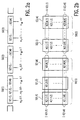
- the DAB method of interleaving at the transmitter side is illustrated in Figure 1 of the application.
- Subsequent samples of a convolutional encoded datastream DB are delayed in accordance with a cyclically repeated delay pattern.
- This delay pattern is represented by an array of 16 rectangles in Figure 1 which functionally represent 16 different delays.
- Each delay is an integral number of times the duration of a frame into which a DAB signal can be subdivided.
- the duration of a frame denoted as FR in Figure 1, can be considered as a unit delay.
- This unit delay depends on the DAB system mode in accordance with which the information is transmitted.
- the unit delay is 24 milliseconds.
- the DAB method of interleaving functionally proceeds as follows.
- a certain sample occurs in the convolutional encoded datastream DB, say sample S1
- the switches SWI and SWO are in a position as shown in Figure 1. Accordingly, sample S1 is delayed zero times the unit delay, that is, sample S1 is not delayed.
- a subsequent sample say sample S2
- switches SWI and SWO have moved one position downwards. Accordingly, sample S2 is delayed eight times the unit delay.
- Switches SWI and SWO continue to move one position downwards at each new, subsequent sample which is delayed in accordance with the numeral in the relevant rectangle in Figure 1.
- the 16th sample S16 occurs the switches will connect the bottom rectangle representing a delay of 15 unit delays.
- switches SWI and SWO return to the position shown in Figure 1. Then, the above-described process is repeated, starting with the 17th sample S17. Accordingly, this sample is not delayed like sample S1, the 18th sample S18 eight times the unit delay, and so on.
- An object of the invention is, to provide a method of interleaving as identified above, which can be performed with a relatively low speed memory. Such a method is defined in Claim 1.
- the invention provides a receiver as defined in Claim 2, a transmitter as defined in Claim 3 an interleaving arrangement as defined in Claim 4, and a memory control unit as defined in Claim 5.
- select lines of a memory are cyclically activated at a cycle rate equal to unit delay.
- both data is written and read from memory locations coupled to the select line.
- the data written comprises a relevant bit of each sample to be delayed in an integral number of sample groups.
- Each sample group is associated with one delay pattern cycle.
- the data read comprises a number of bits which is equal to the number of bits written. The bits are read in accordance with the delay pattern.
- Random accesses are accesses for which two new mutually rectangular select lines, i.e. a row and a column, have to be activated. In a DRAM memory, this requires two clock cycles or more. When only one new select line has to be activated, one clock cycle suffices.
- the average number of clock cycles needed for a memory access is close to one.
- This average number of clock cycles the more relaxed the speed requirement on the memory. This can be explained as follows.
- the sample or bit rate of the digital signal to be interleaved determines the required number of accesses in a given time-span, say, one second.
- a lower speed memory can perform interleaving if the average number of clock cycles for an access is lowered.
- the number of memory locations coupled to a select line i.e. a row or a column
- the number of memory locations coupled to a select line is usually fixed and equals a power of two, for example 512.
- a power of two for example 512.
- not all of these available memory locations will be used in the invention. This is a consequence of writing bits of an integral number of sample groups on a row or a column repetitively each unit delay.
- the integer is the only parameter for varying the total number of bits stored on a row or column.
- there will be no integer with which all available memory locations are used Either the integer is such that some available memory locations are unused, or the integer is such that the number of bits stored exceeds the storage capacity of a row or column.
- the invention provides other notable features. These include low power operation, avoidance of memory refresh cycles, and relatively few and simple address calculations. These and other aspects of the invention will be apparent from and elucidated with reference to the embodiments described hereinafter.
- Figure 2a illustrates the structure of a digital signal to be interleaved.
- the digital signal can be sub-divided into groups of symbols SG(1), SG(2), etc. Each group can be associated with one cycle of a cyclically repeated sample delay pattern.
- the delay pattern for interleaving is as follows. The first sample of this group S(1,1) is to be delayed an integer a1 times a unit delay ⁇ T. The subsequent sample S(1,2) is to be delayed with a delay time of a2 ⁇ T, and so on. Finally, the last sample S(1,M) of symbol group SG(1,M) is to be delayed aM times unit delay ⁇ T. For the next group of samples SG(2), the delay pattern a1 ⁇ T...aM ⁇ T is repeated, accordingly.
- Figure 2b shows the data in symbol group SG(1) in more detail.
- Each sample S(1,1)...S(1,M) consists of N bits, that is, sample S(1,1) comprises bits b(1,1,1), b(1,1,2)...b(1,1,N).
- sample S(1,M) comprises bits b(1,M,1)...b(1,M,N).
- the bits belonging to sample group SG1 can be grouped into interleaving bit groups IG(1,1)...IG(1,N).
- interleaving bit group IG(1,1) comprises bits b(1,1,1), b(1,2,1)..,b(1,M,1).
- Each bit in an interleaving bit group has to be delayed with a unique delay time.
- the delay times which can be associated with each bit in the group correspond to the delay pattern for interleaving.
- bits of a sample there are basically two ways in which bits of a sample can be physically arranged: time-multiplex or line-multiplex.
- time-multiplex arrangement there is one line which carries all the bits of the signal to be interleaved. For example, bits b(1,1,1), b(1,1,2),...b(1,1,N) subsequently occur on the single line, defining the value of sample S(1,1).
- line-multiplex arrangement there are N lines, each line carrying a relevant bit of a sample. For example, bits b(1,1,1), b(1,1,2),...b(1,1,N) occur simultaneously, with each bit on a specific line L1,L2,...Ln, respectively.
- L1,L2,...Ln a specific line L1,L2,...Ln
- Figure 3 illustrates the basic principle of the invention for a case in which sample bits are arranged in line-multiplex.
- input line L(j) carries relevant sample bits of the signal to be interleaved.
- the value of integer j defines which sample bits are involved.
- line L(1) carries bits b(1,1,1), b(1,2,1)...b(1,M,1) of the samples S(1,1), S(1,2)...S(1,M) shown in Figure 2b.
- line L(N) carries bits b(1,1,N)...b(1,M,N).
- a memory MEM is coupled to the line L(j).
- the memory MEM comprises a matrix of select lines, say, horizontal and vertical select lines.
- Each memory location ML is coupled to a specific combination of a horizontal and a vertical select line.
- a specific memory location is accessed when both select lines coupled thereto are activated.
- Figure 3 shows some of the horizontal select lines; the vertical lines are not shown.
- a plurality of X memory locations with X being an integer, is coupled to the horizontal select lines for example, memory locations M(1,1)...M(1,X) are coupled to select line AL(1).
- Each horizontal select line AL(1)...AL(Y) in the memory is cyclically activated at a repetition rate which is equal to unit delay ⁇ T.
- switch HAS which cyclically connects each select line AL(1)..AL(Y) to the line L(j).
- the connection of a select line to lines L(j) via the switch HAS means that this select line is activated. Consequently, data can be written in and read from memory locations coupled to that select line.
- Figure 3 shows a state in which select line AL(1) is activated.
- the method of interleaving proceeds as follows.
- a number of K interleaving bit groups IG(1,j)...IG(K,j) are written in memory locations M(1,1)...M(1,X), K being an integer.
- K being an integer.
- IG(1,j)...IG(K,j) the bit interleaving group IG(1,1) of sample group SG(1) shown in Figure 2b is written.
- Switch HAS continues to move to new positions until after one unit delay ⁇ T it returns to the positions as shown in Figure 3. Then, the cycle is repeated and new data is stored.
- data is also read from memory locations coupled thereto.
- the data can be read in accordance with the interleaving delay pattern. This is possible because the data storage time is an integral number of times unit delay ⁇ T due to the fact that data is cyclically written each unit delay ⁇ T.
- bit interleaving bit groups IG(1,j)...IG(K,j) are written as described above.
- the following data is read from the memory location coupled to select line AL(1).
- the bit corresponding to the bit b(1,1,j) which was written a1 cycles of switch HAS ago is read. This bit is denoted as b(1,1,j)@a1 and has been stored for a duration of a1 ⁇ T.
- a bit corresponding to bit b(1,2,j) is read which has been stored for a duration of a2 ⁇ T, that is, bit b(1,2,j)@a2.
- memory locations become vacant.
- the reading of memory locations precedes the writing when a select line such as, for example, AL(1) is selected.
- the memory locations which have become vacant are used to write new interleaving bit groups, for example, IG(1,j)...IG(K,j) as shown in Figure 3.
- a sample in a sample group does not need to be delayed. It will be evident that the bits of this sample do not need to be stored in the memory MEM shown in Figure 1. For example, let the integer a1 shown in Figure 2a equal zero. In that case, only bits b(1,2,.)...b(1,M,.) of sample group SG(1) are written into memory MEM shown in Figure 3. Bit b(1,1,.) is then no longer part of the bit interleaving groups IG(1,1)..IG(1,N) shown in Figure 2b, which is indicated by the dashed lines. Of course, the same then applies to other bit interleaving groups.
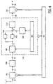
- FIG. 4 shows a DAB receiver in which the interleaving method according to the invention is applied.
- a front-end FRE converts a received DAB modulated carrier RF into an intermediate frequency DAB signal IF from which a demodulation section DEM derives a DAB-demodulated signal DB.
- the DAB-demodulated signal DB is de-interleaved by an interleaving arrangement ILA which will be explained in further detail.
- a decoding section DEC retrieves an error-corrected signal DA, which can be further processed, from the de-interleaved DAB-demodulated signal DD.
- the digital circuitry of the DAB receiver operates under the control of a global controller GLC which, inter alia, ensures that there are no time-conflicts.
- the DAB-demodulated signal DB comprises 4-bit samples which are referred to as metrics in the cited article. Each metric can be associated with a specific sample of the interleaved convolutional encoded datastream DD shown in Figure 1. Hence, the interleaving delay pattern in the receiver should be complementary to that in Figure 1.
- sample groups SG which comprise 16 metrics.
- a capacity unit (CU) in DAB comprises 4 sample groups.
- the DAB baseband signal DB there are bursts of an integral number of CUs at regular time-intervals.
- a buffer memory BME receives CU-bursts in the DAB baseband signal DB and stores the metrics in these bursts.
- a buffer memory BME stores metrics in the DAB-demodulated signal DB and stores these metrics in these bursts.
- the metrics are read from buffer memory BME and transferred to an interleaving memory IME under the control of a memory control unit MCU.
- the memory control unit MCU also controls the read-out of the metrics stored in the interleaving memory IME. This is in conformity with the de-interleaving scheme shown in Figure 1.
- the de-interleaved metrics are supplied to a First In First Out (FIFO) storage device FIF.
- FIFO First In First Out
- the de-interleaved DAB-demodulated signal DD is obtained from the FIFO storage device FIF.
- the interleaving arrangement ILA further comprises two data registers RG1 and RG2 which will be further discussed in the specification.
- the metrics are supplied to and read from the interleaving memory MEM in line-multiplex.
- the interleaving memory IME is a 4x256k DRAM, that is, there are four 256k DRAM units.
- Each of the four bits in a metric is stored in a specific 256k DRAM unit.
- bit b(1,1,1) of metric S(1,1) is stored in a first 256k DRAM unit, bit b(1,1,2) in a second unit, bit b(1,1,3) in a third unit and bit b(1,1,4) in a fourth unit.
- K the number of interleaving bit groups
- interleaving bit groups IG(1,1), IG(2,1), IG(3,1) and IG(4,1) are stored on a single row, that is, the bits b(.,.,1) in the CU are stored on this row.
- the bits b(.,.,2) in this CU are stored on a row in the second 256k DRAM unit.
- this row stores interleaving bit groups IG(1,2), IG(2,2), IG(3,2) and IG(4,2).
- bits b(.,.,3) and b(.,.,4) of the CU are stored in the third and the fourth memory unit, respectively.
- Figure 5 illustrates how the storage of bits on a row R(i) is organized.
- the bits of interleaving bit groups which are to be subjected to the same delay are clustered.
- Clusters 1, 2,...15 comprise bits which are to be delayed a unit delay times the reference numeral of the cluster.
- cluster 15 comprises bits which are to be delayed 15 times unit delay, that is, 15 frames.
- the number of bits in a cluster is 4 times the reference numeral, that is, K times the delay in unit delays.
- cluster 15 comprises 60 bits
- cluster 7 comprises 28 bits, each bit occupying a memory location.
- a total of 480 bits is stored on a row, which means that 480 of the 512 memory locations on a row are effectively used.
- Figures 6a to 6d illustrate the reading and writing of bits on the row R(i).
- Figures 6a to 6d show details near clusters 15 and 7.
- Memory locations are represented by squares. A cross in these memory locations denotes a vacancy.
- bits to be delayed of interleaving bit groups IG(1,1), IG(2,1), IG(3,1) and IG(4,1) shown in Figure 2b are written on row R(i). An equal number of bits are read in accordance with the delay pattern shown in Figure 1.
- bit b(1,1,1)@15 is read from a boundary of cluster 15 which is opposite to the vacant memory location.
- Bit b(1,1,1)@15 corresponds to bit b(1,1,1) and has been written in row R(i) 15 activations of this row ago. Accordingly, bit b(1,1,1)@15 has been stored for 15 unit delays. Due to the above-described writing and reading, cluster 15 moves one position to the left. This is shown in Figure 6b.
- bit b(1,2,1) of interleaving bit group IG(1,1) is written in the memory location which has become vacant due to the reading of bit b(1,1,1)@15.
- a bit b(1,2,1)@7 is read from a memory location in cluster 7 in which it has been stored for 7 unit delays.
- bit b(1,2,1)@7 is at the boundary of cluster 7 opposite to the memory location in which a new bit for cluster 7 is written.
- the memory location from which bit b(1,2,1)@7 is read becomes vacant and is subsequently used to write a following bit b(1,3,1), not shown in Figure 6b.
- Figure 6c shows the position of clusters 15 and 7 at the moment at when all bits of interleaving bit group IG(1,1) are written. All clusters will have moved one position to the left.
- Figure 6c the first bit b(2,1,1) to be delayed of interleaving bit group IG(2,1) is written in a vacant memory location next to the one in which bit(1,1,1) is stored. Similarly to Figure 6a, a corresponding output bit b(2,1,1)@15 is read. Figure 6d shows the next read/write step. Bit b(2,2,1) is written in the memory location previously occupied by bit b(2,1,1)@15. Figure 6d also shows that cluster 15 has again moved one position to the left as compared to Figure 6c similar to Figures 6a and 6b.
- IG(1,2), IG(2,2), IG(3,2) and IG(4,2) are processed likewise in a 256k DRAM unit.
- Figure 7 shows the partitioning of a 256k DRAM unit.
- the partitioning is related to the structure of the DAB-demodulated signal.
- the DAB-demodulated signal may comprise several types of information, for example, a stereo music program and a mono speech channel.
- a number of CUs is assigned to each type of information. The exact number of CUs assigned will, of course, depend on the bit-rate of the type information to be transmitted.
- the stereo music program may occupy 288 CUs in a frame, whereas the mono speech channel occupies 144 CUs.
- rows R(1) to R(288) have been reserved for a first type of information APP1 with 288 CUs per frame.
- Rows R(289) to R(432) are allotted to a second type of information APP2 with 144 CUs per frame.
- the memory locations on rows R(433) to R(486) are used to temporarily store de-interleaved data of a frame.
- Rows R(433) to R(468) and rows R(469) to R(486) constitute frame buffers FRB1 and FRB2, respectively, for the first and the second type of information APP1 and APP2, respectively.
- a relevant metric bit of eight CU's is stored On each row of these frame buffers, that is, 8 times 64 bits which amounts to 512 bits.
- the rows R(487) to R(504) store some DAB-specific data called Fast Information Channel (FIC) which is not further discussed.
- FIC Fast Information Channel
- the de-interleaved data which is read from rows R(1) to R(288) and rows R(289) to R(432), as previously described, is transferred to the respective frame buffer as follows.
- An input metric is read from the buffer memory BME and written into register RG1 prior to storage in the interleaving memory IME. This leaves a vacant memory space in the buffer memory BME.
- four bits are read from the interleaving memory IME and transferred to register RG2. These four bits constitute an output metric for the output signal DD shown in Figure 4. At the next clock cycle this output metric is written into the vacant memory space of buffer memory BME.
- the input metric stored in register RG1 is written into interleaving memory IME.
- FIG 8 shows an example of a DAB transmitter which operates in accordance with the method of interleaving disclosed in this specification.
- this DAB transmitter is a reversed version of the receiver of Figure 4.
- an encoder ENC encodes a digitized audio signal AD.
- the encoding is complementary to the decoding in decoder DEC shown in Figure 4.
- the encoded digital audio signal AE is interleaved in an interleaving arrangement ILA' similar to arrangement ILA shown in Figure 4 and discussed above.
- the interleaved and encoded digital audio signal AI is modulated in accordance with to DAB standards in a modulator MOD.
- the resultant modulated carrier signal MC is frequency-converted and amplified in a high frequency section HFS, to provide a DAB transmission signal TS.
- Relatively low speed memories can be used to perform interleaving.
- the 4x256k DRAM memory operated at a clock frequency of 12,288 Mhz. Due to the memory management as described above a burst of metrics equivalent to 48 CUs occurring every 1,246 msec in the DAB- demodulated signal DB could be processed.
- the power dissipation in the interleaving arrangement shown in Figure 4 is relatively low. This is due to the fact that the clock frequency is relatively low and that only one new select line has to be activated for most memory accesses.
- the memory control unit MCU shown in Figure 4 may be relatively simple. Relatively few column positions have to be calculated during the activation of a row select line. This is due to the fact that most memory locations are accessed to both read and write data. This is shown in Figures 6a to 6b. In Figure 6a, bit b(1,1,1)@15 is read at a certain clock cycle. The next clock cycle bit b(1,2,1) is written in the same memory location as shown in Figure 6b. No new column position has to be determined; the state of the address-generating unit remains unchanged. This is equally favorable for low-power operation.
- the invention may also be used advantageously in receivers other than DAB, for example, in Digital Video Broadcast (DVB) receivers. It may be expected that a typical DVB receiver will equally comprise some form of de-interleaving.
- DVD Digital Video Broadcast
- a row read/write sequence different from the one illustrated in Figures 6a to 6d may be employed. For example, it is possible to first read all the output data before starting a write sequence, or vice versa.
- the integer N may be one. This means that, the signal to be interleaved comprises one-bit samples.
- interleaving memory may be an external RAM as well as an embedded RAM.
Landscapes
- Engineering & Computer Science (AREA)
- Signal Processing (AREA)
- Computer Networks & Wireless Communication (AREA)
- Physics & Mathematics (AREA)
- Probability & Statistics with Applications (AREA)
- Theoretical Computer Science (AREA)
- Error Detection And Correction (AREA)
- Detection And Prevention Of Errors In Transmission (AREA)
- Signal Processing For Digital Recording And Reproducing (AREA)
Abstract
Claims (4)
- Procédé d'entrelacement d'un signal numérique dans lequel des échantillons sont retardés d'un nombre intégral de fois un retard unité (ΔT) selon une configuration de retard (a1,..,aM) répétée cycliquement, caractérisé en ce que ledit procédé comprend les étapes suivantes:l'activation cyclique de lignes de sélection (AL(1)..AL(M)) agencées en parallèle d'une mémoire (MEM) à un débit de cycles qui est égal au retard unité (ΔT);l'écriture de données (IG(1,j)..IG(k,j)) pendant une activation d'une ligne de sélection, lesdites données comprenant un bit significatif de chaque échantillon à retarder dans un nombre intégral de groupes d'échantillons, un groupe d'échantillons étant associé à un cycle de la configuration de retard;la lecture de données ((b(1,1,j)@a1..b(1,M,j)@aM..b(k,1,j)@a1..b(k,M,j)@aM) pendant l'activation de ladite ligne de sélection, lesdites données comprenant un certain nombre de bits étant égal au nombre de bits qui est écrit, lesdits bits étant lus selon la configuration de retard.
- Montage d'entrelacement pour entrelacer un signal numérique dans lequel des échantillons sont retardés d'un nombre intégral de fois un retard unité (ΔT) selon une configuration de retard répétée cycliquement (1a1,..,aM), caractérisé en ce que ledit montage d'entrelacement comporte:des moyens (HAS) pour activer cycliquement des lignes de sélection (AL(1)..AL(M)) d'une mémoire (MEM) à un débit de cycles qui est égal au retard unité (ΔT);des moyens (HAS) pour écrire des données (IG(1,j)..IG(k,j)) pendant une activation d'une ligne de sélection, lesdites données comprenant un bit significatif de chaque échantillon à retarder dans un nombre intégral de groupes d'échantillons, un groupe d'échantillons étant associé à un cycle de la configuration de retard;des moyens (HAS) pour lire des données
(b(1,1,j)@a1..b(1,M,j)@aM..b(k,1,j)@a1..b(k,M,j)@aM) pendant l'activation de ladite ligne de sélection, lesdites données comprenant un certain nombre de bits étant égal au nombre de bits qui est écrit, lesdits bits étant lus selon la configuration de retard. - Récepteur comportant le montage d'entrelacement de la revendication 2 dans lequel lesdits bits étant lus sont en conformité avec une configuration de retard qui est complémentaire de ladite configuration de retard (a1,...,aM).
- Emetteur comportant le montage d'entrelacement de la revendication 2.
Priority Applications (1)
| Application Number | Priority Date | Filing Date | Title |
|---|---|---|---|
| EP95937991A EP0748538B1 (fr) | 1994-12-23 | 1995-12-04 | Entrelacement avec memoire lente |
Applications Claiming Priority (4)
| Application Number | Priority Date | Filing Date | Title |
|---|---|---|---|
| EP94203745 | 1994-12-23 | ||
| EP94203745 | 1994-12-23 | ||
| PCT/IB1995/001088 WO1996020536A1 (fr) | 1994-12-23 | 1995-12-04 | Entrelacement avec memoire lente |
| EP95937991A EP0748538B1 (fr) | 1994-12-23 | 1995-12-04 | Entrelacement avec memoire lente |
Publications (2)
| Publication Number | Publication Date |
|---|---|
| EP0748538A1 EP0748538A1 (fr) | 1996-12-18 |
| EP0748538B1 true EP0748538B1 (fr) | 2002-04-10 |
Family
ID=8217485
Family Applications (1)
| Application Number | Title | Priority Date | Filing Date |
|---|---|---|---|
| EP95937991A Expired - Lifetime EP0748538B1 (fr) | 1994-12-23 | 1995-12-04 | Entrelacement avec memoire lente |
Country Status (6)
| Country | Link |
|---|---|
| US (1) | US6424680B1 (fr) |
| EP (1) | EP0748538B1 (fr) |
| JP (1) | JP3610069B2 (fr) |
| KR (1) | KR100427521B1 (fr) |
| DE (1) | DE69526337T2 (fr) |
| WO (1) | WO1996020536A1 (fr) |
Families Citing this family (9)
| Publication number | Priority date | Publication date | Assignee | Title |
|---|---|---|---|---|
| US5828671A (en) * | 1996-04-10 | 1998-10-27 | Motorola, Inc. | Method and apparatus for deinterleaving an interleaved data stream |
| DE69721495T2 (de) * | 1996-11-11 | 2004-03-18 | Koninklijke Philips Electronics N.V. | Empfänger, entschachtelungsmittel und verfahren zur speicherentschachtelung in verkürzter zeit |
| JP3697833B2 (ja) * | 1997-04-23 | 2005-09-21 | ソニー株式会社 | 放送信号受信装置 |
| JP2958308B1 (ja) | 1998-07-10 | 1999-10-06 | 松下電器産業株式会社 | インターリーブ解除装置 |
| DE19936272C2 (de) * | 1999-07-31 | 2001-09-27 | Bosch Gmbh Robert | Vorrichtung zum Empfang von digitalen Signalen und Vorrichtung zum Senden von digitalen Signalen |
| KR100601624B1 (ko) * | 1999-10-30 | 2006-07-14 | 삼성전자주식회사 | 인터리버빙과 디인터리빙 장치 및 방법 |
| US20050180332A1 (en) * | 2004-02-13 | 2005-08-18 | Broadcom Corporation | Low latency interleaving and deinterleaving |
| EP1607879A1 (fr) * | 2004-06-14 | 2005-12-21 | Dialog Semiconductor GmbH | Entrelacement de mémoire dans un système d'ordinateur |
| KR101491643B1 (ko) | 2013-09-23 | 2015-02-09 | (주)에프씨아이 | 다이버시티 수신장치 |
Family Cites Families (6)
| Publication number | Priority date | Publication date | Assignee | Title |
|---|---|---|---|---|
| US4516219A (en) * | 1981-12-18 | 1985-05-07 | Mitsubishi Denki Kabushiki Kaisha | Address designating method of memory and apparatus therefor |
| US4907215A (en) * | 1986-08-27 | 1990-03-06 | Sony Corporation | Integral optical recording of product code in data areas |
| US5063533A (en) * | 1989-04-10 | 1991-11-05 | Motorola, Inc. | Reconfigurable deinterleaver/interleaver for block oriented data |
| NL8901631A (nl) | 1989-06-28 | 1991-01-16 | Philips Nv | Inrichting voor het bufferen van data voor de duur van cyclisch repeterende buffertijden. |
| US5483541A (en) * | 1993-09-13 | 1996-01-09 | Trw Inc. | Permuted interleaver |
| US5592492A (en) * | 1994-05-13 | 1997-01-07 | Lsi Logic Corporation | Convolutional interleaving/de-interleaving method and apparatus for data transmission |
-
1995
- 1995-12-04 KR KR1019960704723A patent/KR100427521B1/ko not_active IP Right Cessation
- 1995-12-04 WO PCT/IB1995/001088 patent/WO1996020536A1/fr active IP Right Grant
- 1995-12-04 DE DE69526337T patent/DE69526337T2/de not_active Expired - Fee Related
- 1995-12-04 EP EP95937991A patent/EP0748538B1/fr not_active Expired - Lifetime
- 1995-12-04 JP JP52032796A patent/JP3610069B2/ja not_active Expired - Fee Related
- 1995-12-21 US US08/576,544 patent/US6424680B1/en not_active Expired - Fee Related
Also Published As
| Publication number | Publication date |
|---|---|
| WO1996020536A1 (fr) | 1996-07-04 |
| JPH09509818A (ja) | 1997-09-30 |
| JP3610069B2 (ja) | 2005-01-12 |
| KR100427521B1 (ko) | 2004-07-16 |
| DE69526337D1 (de) | 2002-05-16 |
| EP0748538A1 (fr) | 1996-12-18 |
| DE69526337T2 (de) | 2002-12-05 |
| KR970701458A (ko) | 1997-03-17 |
| US6424680B1 (en) | 2002-07-23 |
Similar Documents
| Publication | Publication Date | Title |
|---|---|---|
| US8127199B2 (en) | SDRAM convolutional interleaver with two paths | |
| KR100362090B1 (ko) | 콘벌루셔널인터리버및디인터리버와,그어드레스제네레이터 | |
| EP0748538B1 (fr) | Entrelacement avec memoire lente | |
| EP1253729B1 (fr) | Réduction des effets de scintillement lors d'une transmission optique en espace libre | |
| TWI493973B (zh) | 數位電視訊號解調裝置及其方法 | |
| KR100754077B1 (ko) | 코딩된 저장 심벌 및 부가적인 정보를 사용하여 입력데이터 비트 시퀀스를 인터리빙하는 인터리버 및 방법 | |
| JP3239084B2 (ja) | マルチキャリア伝送インターリーブ装置及び方法 | |
| US6598198B1 (en) | Deinterleaving device that releases a plurality of types of interleaving simultaneously | |
| US6058118A (en) | Method for the dynamic reconfiguration of a time-interleaved signal, with corresponding receiver and signal | |
| EP2242265B1 (fr) | Récepteur de communication sans fil, procédé de réception de communication sans fil et récepteur de télévision | |
| US6192493B1 (en) | Data element interleaving/deinterleaving | |
| JP3804989B2 (ja) | 低減された時間ディインターリーブメモリ用の受信機、ディインターリーブ手段、および方法 | |
| JPH04196822A (ja) | データインタリーブ方式および回路 | |
| US7886203B2 (en) | Method and apparatus for bit interleaving and deinterleaving in wireless communication systems | |
| GB2456292A (en) | Interleaver which reads out and writes into the nth memory address of the previous frames read/write address sequence for each successive frame | |
| JPH11127083A (ja) | 畳込みインタリーバ及びインタリーブ処理方法 | |
| JP3865743B2 (ja) | デジタル放送受信装置、およびデジタル放送受信方法 | |
| EP1089440A1 (fr) | Entrelaceur et méthode d'entrelacment d'une séquence de bits de données | |
| JP3103098B2 (ja) | Pcm音声デコーダ装置 | |
| KR100710223B1 (ko) | 메모리 제어 시스템 및 그 시스템을 이용한 데이터 송수신방법 | |
| CN101500099B (zh) | 无线通讯接收机、无线通讯接收方法与电视接收机 | |
| JPH05284540A (ja) | エンコーダおよびデコーダ | |
| CA2208475C (fr) | Procede de reconfiguration dynamique d'un signal presentant un entrelacement temporel, recepteur et signal correspondants | |
| JPH01280984A (ja) | 衛星データ放送信号受信機 | |
| KR20070058758A (ko) | 시간 디인터리빙 장치 및 방법 |
Legal Events
| Date | Code | Title | Description |
|---|---|---|---|
| PUAI | Public reference made under article 153(3) epc to a published international application that has entered the european phase |
Free format text: ORIGINAL CODE: 0009012 |
|
| AK | Designated contracting states |
Kind code of ref document: A1 Designated state(s): DE FR GB IT |
|
| 17P | Request for examination filed |
Effective date: 19970107 |
|
| 17Q | First examination report despatched |
Effective date: 20000211 |
|
| GRAG | Despatch of communication of intention to grant |
Free format text: ORIGINAL CODE: EPIDOS AGRA |
|
| GRAG | Despatch of communication of intention to grant |
Free format text: ORIGINAL CODE: EPIDOS AGRA |
|
| GRAH | Despatch of communication of intention to grant a patent |
Free format text: ORIGINAL CODE: EPIDOS IGRA |
|
| GRAH | Despatch of communication of intention to grant a patent |
Free format text: ORIGINAL CODE: EPIDOS IGRA |
|
| REG | Reference to a national code |
Ref country code: GB Ref legal event code: IF02 |
|
| GRAA | (expected) grant |
Free format text: ORIGINAL CODE: 0009210 |
|
| AK | Designated contracting states |
Kind code of ref document: B1 Designated state(s): DE FR GB IT |
|
| PG25 | Lapsed in a contracting state [announced via postgrant information from national office to epo] |
Ref country code: IT Free format text: LAPSE BECAUSE OF FAILURE TO SUBMIT A TRANSLATION OF THE DESCRIPTION OR TO PAY THE FEE WITHIN THE PRESCRIBED TIME-LIMIT;WARNING: LAPSES OF ITALIAN PATENTS WITH EFFECTIVE DATE BEFORE 2007 MAY HAVE OCCURRED AT ANY TIME BEFORE 2007. THE CORRECT EFFECTIVE DATE MAY BE DIFFERENT FROM THE ONE RECORDED. Effective date: 20020410 |
|
| RIC1 | Information provided on ipc code assigned before grant |
Free format text: 7H 03M 13/27 A, 7G 11B 20/18 B |
|
| REF | Corresponds to: |
Ref document number: 69526337 Country of ref document: DE Date of ref document: 20020516 |
|
| ET | Fr: translation filed | ||
| ET | Fr: translation filed | ||
| REG | Reference to a national code |
Ref country code: GB Ref legal event code: 746 Effective date: 20020918 |
|
| REG | Reference to a national code |
Ref country code: FR Ref legal event code: D6 |
|
| PLBE | No opposition filed within time limit |
Free format text: ORIGINAL CODE: 0009261 |
|
| STAA | Information on the status of an ep patent application or granted ep patent |
Free format text: STATUS: NO OPPOSITION FILED WITHIN TIME LIMIT |
|
| 26N | No opposition filed |
Effective date: 20030113 |
|
| PGFP | Annual fee paid to national office [announced via postgrant information from national office to epo] |
Ref country code: GB Payment date: 20041222 Year of fee payment: 10 |
|
| PGFP | Annual fee paid to national office [announced via postgrant information from national office to epo] |
Ref country code: FR Payment date: 20041228 Year of fee payment: 10 |
|
| PGFP | Annual fee paid to national office [announced via postgrant information from national office to epo] |
Ref country code: DE Payment date: 20050215 Year of fee payment: 10 |
|
| PG25 | Lapsed in a contracting state [announced via postgrant information from national office to epo] |
Ref country code: GB Free format text: LAPSE BECAUSE OF NON-PAYMENT OF DUE FEES Effective date: 20051204 |
|
| PG25 | Lapsed in a contracting state [announced via postgrant information from national office to epo] |
Ref country code: DE Free format text: LAPSE BECAUSE OF NON-PAYMENT OF DUE FEES Effective date: 20060701 |
|
| GBPC | Gb: european patent ceased through non-payment of renewal fee |
Effective date: 20051204 |
|
| PG25 | Lapsed in a contracting state [announced via postgrant information from national office to epo] |
Ref country code: FR Free format text: LAPSE BECAUSE OF NON-PAYMENT OF DUE FEES Effective date: 20060831 |
|
| REG | Reference to a national code |
Ref country code: FR Ref legal event code: ST Effective date: 20060831 |