EP0748538B1 - Interleaving with low-speed memory - Google Patents

Interleaving with low-speed memory Download PDF

Info

Publication number
EP0748538B1
EP0748538B1 EP95937991A EP95937991A EP0748538B1 EP 0748538 B1 EP0748538 B1 EP 0748538B1 EP 95937991 A EP95937991 A EP 95937991A EP 95937991 A EP95937991 A EP 95937991A EP 0748538 B1 EP0748538 B1 EP 0748538B1
Authority
EP
European Patent Office
Prior art keywords
interleaving
bits
memory
sample
bit
Prior art date
Legal status (The legal status is an assumption and is not a legal conclusion. Google has not performed a legal analysis and makes no representation as to the accuracy of the status listed.)
Expired - Lifetime
Application number
EP95937991A
Other languages
German (de)
French (fr)
Other versions
EP0748538A1 (en
Inventor
Antoine Delaruelle
Franciscus Antonius Maria Van De Laar
Current Assignee (The listed assignees may be inaccurate. Google has not performed a legal analysis and makes no representation or warranty as to the accuracy of the list.)
Koninklijke Philips NV
Original Assignee
Koninklijke Philips Electronics NV
Priority date (The priority date is an assumption and is not a legal conclusion. Google has not performed a legal analysis and makes no representation as to the accuracy of the date listed.)
Filing date
Publication date
Application filed by Koninklijke Philips Electronics NV filed Critical Koninklijke Philips Electronics NV
Priority to EP95937991A priority Critical patent/EP0748538B1/en
Publication of EP0748538A1 publication Critical patent/EP0748538A1/en
Application granted granted Critical
Publication of EP0748538B1 publication Critical patent/EP0748538B1/en
Anticipated expiration legal-status Critical
Expired - Lifetime legal-status Critical Current

Links

Images

Classifications

    • HELECTRICITY
    • H03ELECTRONIC CIRCUITRY
    • H03MCODING; DECODING; CODE CONVERSION IN GENERAL
    • H03M13/00Coding, decoding or code conversion, for error detection or error correction; Coding theory basic assumptions; Coding bounds; Error probability evaluation methods; Channel models; Simulation or testing of codes
    • H03M13/27Coding, decoding or code conversion, for error detection or error correction; Coding theory basic assumptions; Coding bounds; Error probability evaluation methods; Channel models; Simulation or testing of codes using interleaving techniques
    • HELECTRICITY
    • H04ELECTRIC COMMUNICATION TECHNIQUE
    • H04HBROADCAST COMMUNICATION
    • H04H20/00Arrangements for broadcast or for distribution combined with broadcast
    • H04H20/44Arrangements characterised by circuits or components specially adapted for broadcast
    • H04H20/46Arrangements characterised by circuits or components specially adapted for broadcast specially adapted for broadcast systems covered by groups H04H20/53-H04H20/95
    • HELECTRICITY
    • H03ELECTRONIC CIRCUITRY
    • H03MCODING; DECODING; CODE CONVERSION IN GENERAL
    • H03M13/00Coding, decoding or code conversion, for error detection or error correction; Coding theory basic assumptions; Coding bounds; Error probability evaluation methods; Channel models; Simulation or testing of codes
    • H03M13/27Coding, decoding or code conversion, for error detection or error correction; Coding theory basic assumptions; Coding bounds; Error probability evaluation methods; Channel models; Simulation or testing of codes using interleaving techniques
    • H03M13/2732Convolutional interleaver; Interleavers using shift-registers or delay lines like, e.g. Ramsey type interleaver
    • HELECTRICITY
    • H04ELECTRIC COMMUNICATION TECHNIQUE
    • H04HBROADCAST COMMUNICATION
    • H04H40/00Arrangements specially adapted for receiving broadcast information
    • H04H40/18Arrangements characterised by circuits or components specially adapted for receiving
    • H04H40/27Arrangements characterised by circuits or components specially adapted for receiving specially adapted for broadcast systems covered by groups H04H20/53 - H04H20/95
    • HELECTRICITY
    • H04ELECTRIC COMMUNICATION TECHNIQUE
    • H04LTRANSMISSION OF DIGITAL INFORMATION, e.g. TELEGRAPHIC COMMUNICATION
    • H04L1/00Arrangements for detecting or preventing errors in the information received
    • H04L1/004Arrangements for detecting or preventing errors in the information received by using forward error control
    • H04L1/0041Arrangements at the transmitter end
    • H04L1/0043Realisations of complexity reduction techniques, e.g. use of look-up tables
    • HELECTRICITY
    • H04ELECTRIC COMMUNICATION TECHNIQUE
    • H04LTRANSMISSION OF DIGITAL INFORMATION, e.g. TELEGRAPHIC COMMUNICATION
    • H04L1/00Arrangements for detecting or preventing errors in the information received
    • H04L1/004Arrangements for detecting or preventing errors in the information received by using forward error control
    • H04L1/0045Arrangements at the receiver end
    • H04L1/0052Realisations of complexity reduction techniques, e.g. pipelining or use of look-up tables
    • HELECTRICITY
    • H04ELECTRIC COMMUNICATION TECHNIQUE
    • H04LTRANSMISSION OF DIGITAL INFORMATION, e.g. TELEGRAPHIC COMMUNICATION
    • H04L1/00Arrangements for detecting or preventing errors in the information received
    • H04L1/004Arrangements for detecting or preventing errors in the information received by using forward error control
    • H04L1/0056Systems characterized by the type of code used
    • H04L1/0071Use of interleaving
    • HELECTRICITY
    • H04ELECTRIC COMMUNICATION TECHNIQUE
    • H04LTRANSMISSION OF DIGITAL INFORMATION, e.g. TELEGRAPHIC COMMUNICATION
    • H04L27/00Modulated-carrier systems
    • H04L27/26Systems using multi-frequency codes
    • H04L27/2601Multicarrier modulation systems
    • H04L27/2647Arrangements specific to the receiver only
    • HELECTRICITY
    • H04ELECTRIC COMMUNICATION TECHNIQUE
    • H04HBROADCAST COMMUNICATION
    • H04H20/00Arrangements for broadcast or for distribution combined with broadcast
    • H04H20/65Arrangements characterised by transmission systems for broadcast
    • H04H20/71Wireless systems
    • H04H20/72Wireless systems of terrestrial networks
    • HELECTRICITY
    • H04ELECTRIC COMMUNICATION TECHNIQUE
    • H04HBROADCAST COMMUNICATION
    • H04H2201/00Aspects of broadcast communication
    • H04H2201/10Aspects of broadcast communication characterised by the type of broadcast system
    • H04H2201/20Aspects of broadcast communication characterised by the type of broadcast system digital audio broadcasting [DAB]

Abstract

A digital signal is interleaved by delaying samples thereof an integral number of times a unit delay (ΔT) in accordance with a cyclically repeated delay pattern (a1,..,aM). Select lines (AL(1)..AL(M)) of a memory (MEM) are cyclically activated (HAS) at a cycle rate equal to unit delay (ΔT). During the activation (HAS) of a select line (AL(1)..AL(M)), both data is written and read from the memory. The data written (IG(1,j)..IG(k,j)) comprises a relevant bit of each sample to be delayed in an integral number of sample groups. Each sample group is associated with one delay pattern cycle. The data read (b(1,1,j)@al..b(1,M,j)@aM..b(k,1,j)@al..b(k,M,j)@aM) comprises a number of bits which is equal to the number of bits written. The bits are read in accordance with the delay pattern. Accordingly, the speed requirements imposed on the memory (MEM) are relatively lax.

Description

The invention relates to a method of interleaving. Interleaving is the process of changing the sequence of samples in a data stream.
The invention may be used, inter alia, in receivers and transmitters, in particular for Digital Audio Broadcast (DAB) or Digital Video Broadcast receiver (DVB). In a transmitter, a digital signal to be transmitted can be interleaved. Accordingly, in a corresponding receiver, a digital baseband signal should be in a manner interleaved complementary to restore the original sequence of samples. In information transmission, interleaving helps to counteract deficiencies in the channel via which the information is transmitted. For example, in mobile reception of a radio signal there is fading which may cause a burst of errors in the demodulated signal. These errors are dispersed by interleaving the demodulated signal. Dispersed errors can be corrected by means of appropriate decoding techniques.
The invention may be embodied in an interleaving arrangement comprising a memory and a memory control unit. The invention may also be embodied in a memory control unit as such, for example, in the form of an integrated circuit. The memory control unit itself may comprise a memory in which instructions are stored for carrying out a method of interleaving according to the invention.
More specifically, the invention relates to a method of interleaving a digital signal as defined in the pre-characterizing part of Claim 1. Such a method is part of a DAB standard laid down in ETSI PRETS 3041 Final Draft. According to the DAB standard, a convolutional encoded datastream is interleaved at the transmitter side. The process of restoring the original sample sequence at the receiving side is referred to as de-interleaving. It should be noted that in this specification the term interleaving is used as a generic term which also includes de-interleaving.
The DAB method of interleaving at the transmitter side is illustrated in Figure 1 of the application. Subsequent samples of a convolutional encoded datastream DB are delayed in accordance with a cyclically repeated delay pattern. This delay pattern is represented by an array of 16 rectangles in Figure 1 which functionally represent 16 different delays. Each delay is an integral number of times the duration of a frame into which a DAB signal can be subdivided. The duration of a frame, denoted as FR in Figure 1, can be considered as a unit delay. This unit delay depends on the DAB system mode in accordance with which the information is transmitted. The unit delay is 24 milliseconds.
The DAB method of interleaving functionally proceeds as follows. When a certain sample occurs in the convolutional encoded datastream DB, say sample S1, the switches SWI and SWO are in a position as shown in Figure 1. Accordingly, sample S1 is delayed zero times the unit delay, that is, sample S1 is not delayed. When a subsequent sample occurs, say sample S2, switches SWI and SWO have moved one position downwards. Accordingly, sample S2 is delayed eight times the unit delay. Switches SWI and SWO continue to move one position downwards at each new, subsequent sample which is delayed in accordance with the numeral in the relevant rectangle in Figure 1. When the 16th sample S16 occurs the switches will connect the bottom rectangle representing a delay of 15 unit delays. Subsequent to this position, switches SWI and SWO return to the position shown in Figure 1. Then, the above-described process is repeated, starting with the 17th sample S17. Accordingly, this sample is not delayed like sample S1, the 18th sample S18 eight times the unit delay, and so on.
An object of the invention is, to provide a method of interleaving as identified above, which can be performed with a relatively low speed memory. Such a method is defined in Claim 1. In addition, the invention provides a receiver as defined in Claim 2, a transmitter as defined in Claim 3 an interleaving arrangement as defined in Claim 4, and a memory control unit as defined in Claim 5.
Briefly, in the invention select lines of a memory are cyclically activated at a cycle rate equal to unit delay. During the activation of a select line both data is written and read from memory locations coupled to the select line. The data written comprises a relevant bit of each sample to be delayed in an integral number of sample groups. Each sample group is associated with one delay pattern cycle. The data read comprises a number of bits which is equal to the number of bits written. The bits are read in accordance with the delay pattern.
Accordingly, for most memory accesses a newly accessed memory location is coupled to an identical select line as the previously accessed memory location. Such accesses require one clock cycle. In the invention random accesses are kept to a minimum. Random accesses are accesses for which two new mutually rectangular select lines, i.e. a row and a column, have to be activated. In a DRAM memory, this requires two clock cycles or more. When only one new select line has to be activated, one clock cycle suffices.
Hence, in the invention the average number of clock cycles needed for a memory access is close to one. The lower this average number of clock cycles, the more relaxed the speed requirement on the memory. This can be explained as follows.
The sample or bit rate of the digital signal to be interleaved determines the required number of accesses in a given time-span, say, one second. The higher the average number of clock cycles for a memory access, the more clock cycles are needed in one second to effectuate the required number of accesses. This means that the needs to be higher, because the clock frequency is equal to the number of clock cycles in one second. Hence, a lower speed memory can perform interleaving if the average number of clock cycles for an access is lowered.
It may seem illogical that the storage capacity of the memory is not fully exploited, which will be the case in most practical applications of the invention. In commercially available memories, the number of memory locations coupled to a select line, i.e. a row or a column, is usually fixed and equals a power of two, for example 512. Generally, not all of these available memory locations will be used in the invention. This is a consequence of writing bits of an integral number of sample groups on a row or a column repetitively each unit delay. The integer is the only parameter for varying the total number of bits stored on a row or column. Generally, there will be no integer with which all available memory locations are used. Either the integer is such that some available memory locations are unused, or the integer is such that the number of bits stored exceeds the storage capacity of a row or column.
In addition to interleaving with low speed memories, the invention provides other notable features. These include low power operation, avoidance of memory refresh cycles, and relatively few and simple address calculations. These and other aspects of the invention will be apparent from and elucidated with reference to the embodiments described hereinafter.
In the drawings:
  • Figure 1 illustrates interleaving of a convolutional encoded datastream in DAB.
  • Figures 2a and 2b show the structure of a datastream to be interleaved.
  • Figure 3 illustrates the basic principle of the invention.
  • Figure 4 is an example of a receiver according to the invention in a block-schematic diagram.
  • Figure 5 illustrates the partitioning of data on a row of an interleaving memory.
  • Figures 6a to 6d illustrate the reading and writing of data on the row.
  • Figure 7 illustrates the partitioning of data in the interleaving memory for a DAB application.
  • Figure 8 is an example of a transmitter according to the invention in a block-schematic diagram.
  • First, the basic principle of the invention will be further explained. Next, an application of the invention in a DAB receiver will be described by way of example. Subsequently, notable features of the invention will be highlighted with reference to this example. Finally, some variants of the example shown will be dealt with.
    Figure 2a illustrates the structure of a digital signal to be interleaved. The digital signal can be sub-divided into groups of symbols SG(1), SG(2), etc. Each group can be associated with one cycle of a cyclically repeated sample delay pattern. Referring to symbol group SG(1), the delay pattern for interleaving is as follows. The first sample of this group S(1,1) is to be delayed an integer a1 times a unit delay ΔT. The subsequent sample S(1,2) is to be delayed with a delay time of a2·ΔT, and so on. Finally, the last sample S(1,M) of symbol group SG(1,M) is to be delayed aM times unit delay ΔT. For the next group of samples SG(2), the delay pattern a1·ΔT...aM·ΔT is repeated, accordingly.
    Figure 2b shows the data in symbol group SG(1) in more detail. Each sample S(1,1)...S(1,M) consists of N bits, that is, sample S(1,1) comprises bits b(1,1,1), b(1,1,2)...b(1,1,N). Similarly, sample S(1,M) comprises bits b(1,M,1)...b(1,M,N). The bits belonging to sample group SG1 can be grouped into interleaving bit groups IG(1,1)...IG(1,N). For each sample S(1,1)..S(1,M) one bit is taken to form such an interleaving bit group. For example, interleaving bit group IG(1,1) comprises bits b(1,1,1), b(1,2,1)..,b(1,M,1). Each bit in an interleaving bit group has to be delayed with a unique delay time. Moreover, the delay times which can be associated with each bit in the group correspond to the delay pattern for interleaving.
    It should be noted that there are basically two ways in which bits of a sample can be physically arranged: time-multiplex or line-multiplex. In a time-multiplex arrangement there is one line which carries all the bits of the signal to be interleaved. For example, bits b(1,1,1), b(1,1,2),...b(1,1,N) subsequently occur on the single line, defining the value of sample S(1,1). In a line-multiplex arrangement there are N lines, each line carrying a relevant bit of a sample. For example, bits b(1,1,1), b(1,1,2),...b(1,1,N) occur simultaneously, with each bit on a specific line L1,L2,...Ln, respectively. Of course, it is possible to conceive intermediate ways of physically arranging sample bits.
    Figure 3 illustrates the basic principle of the invention for a case in which sample bits are arranged in line-multiplex. In Figure 3, input line L(j) carries relevant sample bits of the signal to be interleaved. The value of integer j defines which sample bits are involved. For example, line L(1) carries bits b(1,1,1), b(1,2,1)...b(1,M,1) of the samples S(1,1), S(1,2)...S(1,M) shown in Figure 2b. Accordingly, line L(N) carries bits b(1,1,N)...b(1,M,N).
    A memory MEM is coupled to the line L(j). The memory MEM comprises a matrix of select lines, say, horizontal and vertical select lines. Each memory location ML is coupled to a specific combination of a horizontal and a vertical select line. A specific memory location is accessed when both select lines coupled thereto are activated. Figure 3 shows some of the horizontal select lines; the vertical lines are not shown. A plurality of X memory locations with X being an integer, is coupled to the horizontal select lines for example, memory locations M(1,1)...M(1,X) are coupled to select line AL(1).
    Each horizontal select line AL(1)...AL(Y) in the memory is cyclically activated at a repetition rate which is equal to unit delay ΔT. This is visualized in Figure 3 by means of switch HAS which cyclically connects each select line AL(1)..AL(Y) to the line L(j). The connection of a select line to lines L(j) via the switch HAS means that this select line is activated. Consequently, data can be written in and read from memory locations coupled to that select line. Figure 3 shows a state in which select line AL(1) is activated.
    The method of interleaving proceeds as follows. In the state shown in Figure 3, a number of K interleaving bit groups IG(1,j)...IG(K,j) are written in memory locations M(1,1)...M(1,X), K being an integer. This is visualized in Figure 3 by an arrow pointing towards memory MEM denoted by IG(1,j)...IG(K,j). For example, if j=1, the bit interleaving group IG(1,1) of sample group SG(1) shown in Figure 2b is written. If, in addition, K=2, the interleaving bit group IG(2,1) is equally written.
    When switch HAS has moved one position downwards, select line AL(2) is activated. In that state, the following K bit interleaving groups IG(K+ 1,j)...IG(2·K,j) are written in memory locations coupled to select line AL(2). For example, if j =1 and K=1, bit interleaving group IG(2,1) shown in Figure 2b is written in memory locations coupled to select line AL(1). However, if K had equalled 2, bit interleaving groups IG(3,1) and IG(4,1), not shown in Figure 2b, would have been written.
    Switch HAS continues to move to new positions until after one unit delay ΔT it returns to the positions as shown in Figure 3. Then, the cycle is repeated and new data is stored.
    During the activation of a select line, data is also read from memory locations coupled thereto. The data can be read in accordance with the interleaving delay pattern. This is possible because the data storage time is an integral number of times unit delay ΔT due to the fact that data is cyclically written each unit delay ΔT.
    For example, consider the state shown in Figure 3 in which bit interleaving bit groups IG(1,j)...IG(K,j) are written as described above. In accordance with the delay pattern a1·ΔT...aM·ΔT of Figure 2a, the following data is read from the memory location coupled to select line AL(1). First, the bit corresponding to the bit b(1,1,j) which was written a1 cycles of switch HAS ago is read. This bit is denoted as b(1,1,j)@a1 and has been stored for a duration of a1·ΔT. Subsequently, a bit corresponding to bit b(1,2,j) is read which has been stored for a duration of a2·T, that is, bit b(1,2,j)@a2. Accordingly, other memory locations in which bits b(1,3,j)@a3...b(1,M,j)@aM have been stored are read. If K is larger than one, the same relevant delayed bits are read which correspond to the interleaving bit group IG(2,j). The read-out is generically illustrated in Figure 3 by an arrow pointing away from memory MEM denoted as b(1,1,j)@a1..b(1,M,j)@aM...b(K,1,j)@a1..b(K,M,j)@aM.
    As a result of reading storage data as described above, memory locations become vacant. Advantageously, the reading of memory locations precedes the writing when a select line such as, for example, AL(1) is selected. The memory locations which have become vacant are used to write new interleaving bit groups, for example, IG(1,j)...IG(K,j) as shown in Figure 3.
    In principle, it does not matter in which memory locations individual bits of an interleaving bit group are actually written. Of course, relevant data which is to be read in one of the following activations of a horizontal select line should not be overwritten. The actual memory locations from which bits are read and in which bits are written are determined by the activation of the vertical select lines not shown in Figure 3. The scheme of this activation will be further referred to as a vertical addressing scheme. The vertical addressing scheme should, of course, be in conformity with the desired interleaving delay pattern. In a sense, it must keep track of the storage time of the data to read the correct sequence of output bits. An advantageous vertical addressing scheme has been described in PHN 13.007 and will not be discussed in further detail.
    In some cases, a sample in a sample group does not need to be delayed. It will be evident that the bits of this sample do not need to be stored in the memory MEM shown in Figure 1. For example, let the integer a1 shown in Figure 2a equal zero. In that case, only bits b(1,2,.)...b(1,M,.) of sample group SG(1) are written into memory MEM shown in Figure 3. Bit b(1,1,.) is then no longer part of the bit interleaving groups IG(1,1)..IG(1,N) shown in Figure 2b, which is indicated by the dashed lines. Of course, the same then applies to other bit interleaving groups.
    However, even if one bit of an interleaving bit group does not need to be delayed, it can nevertheless be stored. All integers a1..aM can be augmented with the same amount without this affecting the interleaving as such. The only effect will be an additional delay in the output signal as a result of interleaving.
    By way of example, an application of the invention in a DAB receiver will now be presented. For details on DAB reference is made to the article "Specification, Partitioning and Design of a DAB channel decoder" in IEEE Special Publication VLSI Signal Processing VI, pp. 21-29.
    Figure 4 shows a DAB receiver in which the interleaving method according to the invention is applied. A front-end FRE converts a received DAB modulated carrier RF into an intermediate frequency DAB signal IF from which a demodulation section DEM derives a DAB-demodulated signal DB. The DAB-demodulated signal DB is de-interleaved by an interleaving arrangement ILA which will be explained in further detail. A decoding section DEC retrieves an error-corrected signal DA, which can be further processed, from the de-interleaved DAB-demodulated signal DD. The digital circuitry of the DAB receiver operates under the control of a global controller GLC which, inter alia, ensures that there are no time-conflicts.
    The DAB-demodulated signal DB comprises 4-bit samples which are referred to as metrics in the cited article. Each metric can be associated with a specific sample of the interleaved convolutional encoded datastream DD shown in Figure 1. Hence, the interleaving delay pattern in the receiver should be complementary to that in Figure 1.
    The DAB-demodulated signal has a structure as shown in Figure 2a with M=16, N=4 and unit delay ΔT being one frame duration. Thus, there are sample groups SG which comprise 16 metrics. The integers a1, a2,...a16 are defined in accordance with a delay pattern which is complementary to the delay pattern at the transmitter side shown in Figure 1. This means that a1=15, a2=7, a3=11,...,a15=8 and a16=0 when sample S(1,1) shown in Figure 2a is associated with sample S1 in Figure 1.
    It should be noted that a capacity unit (CU) in DAB comprises 4 sample groups. Hence, a CU comprise 4x16=64 metrics. In the DAB baseband signal DB there are bursts of an integral number of CUs at regular time-intervals.
    In the interleaving arrangement ILA, a buffer memory BME receives CU-bursts in the DAB baseband signal DB and stores the metrics in these bursts. In the interleaving arrangement ILA, a buffer memory BME stores metrics in the DAB-demodulated signal DB and stores these metrics in these bursts. The metrics are read from buffer memory BME and transferred to an interleaving memory IME under the control of a memory control unit MCU. The memory control unit MCU also controls the read-out of the metrics stored in the interleaving memory IME. This is in conformity with the de-interleaving scheme shown in Figure 1. The de-interleaved metrics are supplied to a First In First Out (FIFO) storage device FIF. This is done to spread the de-interleaved metrics read from the memory in a burst-like fashion more uniformly in time. The de-interleaved DAB-demodulated signal DD is obtained from the FIFO storage device FIF. The interleaving arrangement ILA further comprises two data registers RG1 and RG2 which will be further discussed in the specification.
    The metrics are supplied to and read from the interleaving memory MEM in line-multiplex. The interleaving memory IME is a 4x256k DRAM, that is, there are four 256k DRAM units. Each of the four bits in a metric is stored in a specific 256k DRAM unit. For example, referring to Figure 2a for which in DAB n=4 and M=16, bit b(1,1,1) of metric S(1,1) is stored in a first 256k DRAM unit, bit b(1,1,2) in a second unit, bit b(1,1,3) in a third unit and bit b(1,1,4) in a fourth unit. Each 256k DRAM unit has 512 columns and 512 rows, each column and row having its own select line. Referring to Figure 3, in this application AL(1)..AL(Y) are row select lines for which X=512.
    One CU is written on each row of a 256k DRAM unit for each activation of the row select line, that is, four interleaving bit groups are written: K=4. For example, referring to Figure 2a, let sample groups SG(1), SG(2), SG(3) and SG(4) constitute a CU in DAB. In the first 256k DRAM unit, interleaving bit groups IG(1,1), IG(2,1), IG(3,1) and IG(4,1) are stored on a single row, that is, the bits b(.,.,1) in the CU are stored on this row. The bits b(.,.,2) in this CU are stored on a row in the second 256k DRAM unit. Hence, this row stores interleaving bit groups IG(1,2), IG(2,2), IG(3,2) and IG(4,2). Similarly, bits b(.,.,3) and b(.,.,4) of the CU are stored in the third and the fourth memory unit, respectively.
    Figure 5 illustrates how the storage of bits on a row R(i) is organized. The bits of interleaving bit groups which are to be subjected to the same delay are clustered. Clusters 1, 2,...15 comprise bits which are to be delayed a unit delay times the reference numeral of the cluster. For example, cluster 15 comprises bits which are to be delayed 15 times unit delay, that is, 15 frames. The number of bits in a cluster is 4 times the reference numeral, that is, K times the delay in unit delays. Accordingly, cluster 15 comprises 60 bits, cluster 7 comprises 28 bits, each bit occupying a memory location. A total of 480 bits is stored on a row, which means that 480 of the 512 memory locations on a row are effectively used.
    Figures 6a to 6d illustrate the reading and writing of bits on the row R(i). Figures 6a to 6d show details near clusters 15 and 7. Memory locations are represented by squares. A cross in these memory locations denotes a vacancy. During the activation of the row select line, bits to be delayed of interleaving bit groups IG(1,1), IG(2,1), IG(3,1) and IG(4,1) shown in Figure 2b are written on row R(i). An equal number of bits are read in accordance with the delay pattern shown in Figure 1.
    In Figure 6a, the first bit to be delayed b(1,1,1) is written in a vacant memory location adjacent to cluster 15. Further, a bit b(1,1,1)@15 is read from a boundary of cluster 15 which is opposite to the vacant memory location. Bit b(1,1,1)@15 corresponds to bit b(1,1,1) and has been written in row R(i) 15 activations of this row ago. Accordingly, bit b(1,1,1)@15 has been stored for 15 unit delays. Due to the above-described writing and reading, cluster 15 moves one position to the left. This is shown in Figure 6b.
    In Figure 6b, the next bit b(1,2,1) of interleaving bit group IG(1,1) is written in the memory location which has become vacant due to the reading of bit b(1,1,1)@15. Subsequently, a bit b(1,2,1)@7 is read from a memory location in cluster 7 in which it has been stored for 7 unit delays. Similarly to bit b(1,1,1)@15 in cluster 15, bit b(1,2,1)@7 is at the boundary of cluster 7 opposite to the memory location in which a new bit for cluster 7 is written. The memory location from which bit b(1,2,1)@7 is read becomes vacant and is subsequently used to write a following bit b(1,3,1), not shown in Figure 6b. This process of reading and writing bit-by-bit continues likewise for the other clusters on row R(i). Figure 6c shows the position of clusters 15 and 7 at the moment at when all bits of interleaving bit group IG(1,1) are written. All clusters will have moved one position to the left.
    In Figure 6c, the first bit b(2,1,1) to be delayed of interleaving bit group IG(2,1) is written in a vacant memory location next to the one in which bit(1,1,1) is stored. Similarly to Figure 6a, a corresponding output bit b(2,1,1)@15 is read. Figure 6d shows the next read/write step. Bit b(2,2,1) is written in the memory location previously occupied by bit b(2,1,1)@15. Figure 6d also shows that cluster 15 has again moved one position to the left as compared to Figure 6c similar to Figures 6a and 6b.
    When all bits of interleaving bit groups IG(1,1), IG(2,1), IG(3,1) and IG(4,1) have been stored, all clusters on row R(i) will have moved four positions to the left. A new select line of a new row is then activated and a similar read/write process takes place on this row. This row-by-row read/write process continues until row R(i) is newly selected after one unit delay and the read/write process is repeated with new data being written and read. After 7 cycles with reference to figure 6a to 6d, bit b(1,2,1) will be read. This bit will then be at the right-hand boundary of cluster 7. It will be clear that all clusters move in the process of interleaving.
    Other relevant bits in sample groups, for example IG(1,2), IG(2,2), IG(3,2) and IG(4,2), are processed likewise in a 256k DRAM unit.
    Figure 7 shows the partitioning of a 256k DRAM unit. The partitioning is related to the structure of the DAB-demodulated signal. The DAB-demodulated signal may comprise several types of information, for example, a stereo music program and a mono speech channel. In a frame, a number of CUs is assigned to each type of information. The exact number of CUs assigned will, of course, depend on the bit-rate of the type information to be transmitted. For example, the stereo music program may occupy 288 CUs in a frame, whereas the mono speech channel occupies 144 CUs.
    In Figure 7, rows R(1) to R(288) have been reserved for a first type of information APP1 with 288 CUs per frame. Rows R(289) to R(432) are allotted to a second type of information APP2 with 144 CUs per frame. The memory locations on rows R(433) to R(486) are used to temporarily store de-interleaved data of a frame. Rows R(433) to R(468) and rows R(469) to R(486) constitute frame buffers FRB1 and FRB2, respectively, for the first and the second type of information APP1 and APP2, respectively. A relevant metric bit of eight CU's is stored On each row of these frame buffers, that is, 8 times 64 bits which amounts to 512 bits. The rows R(487) to R(504) store some DAB-specific data called Fast Information Channel (FIC) which is not further discussed.
    The de-interleaved data which is read from rows R(1) to R(288) and rows R(289) to R(432), as previously described, is transferred to the respective frame buffer as follows. An input metric is read from the buffer memory BME and written into register RG1 prior to storage in the interleaving memory IME. This leaves a vacant memory space in the buffer memory BME. Simultaneously, four bits are read from the interleaving memory IME and transferred to register RG2. These four bits constitute an output metric for the output signal DD shown in Figure 4. At the next clock cycle this output metric is written into the vacant memory space of buffer memory BME. At the same clock cycle, the input metric stored in register RG1 is written into interleaving memory IME.
    The above-described transfer of metrics continues until all input metrics in the buffer memory BME are replaced by output metrics from the interleaving memory IME. Then, the output metrics are transferred from the buffer memory BME and written in the appropriate frame buffer of interleaving memory IME. Time-conflict is avoided by the global controller GLC shown in Figure 4. Not all CUs in the DAB- demodulated signal DB need to be processed. During a period in which non-relevant data is supplied by the demodulation section DEM, the above-described internal transfer of data in the interleaving arrangement ILA is effected.
    Figure 8 shows an example of a DAB transmitter which operates in accordance with the method of interleaving disclosed in this specification. In a sense, this DAB transmitter is a reversed version of the receiver of Figure 4. In Figure 8, an encoder ENC encodes a digitized audio signal AD. The encoding is complementary to the decoding in decoder DEC shown in Figure 4. The encoded digital audio signal AE is interleaved in an interleaving arrangement ILA' similar to arrangement ILA shown in Figure 4 and discussed above. The interleaved and encoded digital audio signal AI is modulated in accordance with to DAB standards in a modulator MOD. The resultant modulated carrier signal MC is frequency-converted and amplified in a high frequency section HFS, to provide a DAB transmission signal TS.
    Some notable features of the invention will be described with reference to the examples shown.
    Relatively low speed memories can be used to perform interleaving. In an experimental DAB receiver shown in Figure 4, the 4x256k DRAM memory operated at a clock frequency of 12,288 Mhz. Due to the memory management as described above a burst of metrics equivalent to 48 CUs occurring every 1,246 msec in the DAB- demodulated signal DB could be processed.
    The power dissipation in the interleaving arrangement shown in Figure 4 is relatively low. This is due to the fact that the clock frequency is relatively low and that only one new select line has to be activated for most memory accesses.
    No refresh cycles have to be provided for the rows 1 to 432 shown in Figure 7. Due to the fact that the rows are cyclically selected each unit delay, for DAB 24 milliseconds, the data stored in these rows is automatically refreshed.
    The memory control unit MCU shown in Figure 4 may be relatively simple. Relatively few column positions have to be calculated during the activation of a row select line. This is due to the fact that most memory locations are accessed to both read and write data. This is shown in Figures 6a to 6b. In Figure 6a, bit b(1,1,1)@15 is read at a certain clock cycle. The next clock cycle bit b(1,2,1) is written in the same memory location as shown in Figure 6b. No new column position has to be determined; the state of the address-generating unit remains unchanged. This is equally favorable for low-power operation.
    The storage capacity of the 4X256k DRAM interleaving memory IME in Figure 4 is used relatively efficiently. Of the 512 memory locations on rows 1 to 432, 480 are used effectively. It should be noted that the number of memory locations used effectively (NML) can be calculated in accordance with the following formula: NML=K·M·AD, in which AD is the average delay of an interleaving delay pattern. For DAB M=16 and AD=7,5, AD can be readily derived from Figure 1. By choosing K=4, the percentage of unused storage capacity is kept to a minimum.
    The invention may also be used advantageously in receivers other than DAB, for example, in Digital Video Broadcast (DVB) receivers. It may be expected that a typical DVB receiver will equally comprise some form of de-interleaving.
    A row read/write sequence different from the one illustrated in Figures 6a to 6d may be employed. For example, it is possible to first read all the output data before starting a write sequence, or vice versa.
    Referring to Figure 2b, it will be clear that the integer N may be one. This means that, the signal to be interleaved comprises one-bit samples.
    It will also be clear that the interleaving memory may be an external RAM as well as an embedded RAM.
    It will be evident that where the term select line is used in this specification, this term may alternatively be replaced by row or column. Any reference signs in a Claim cannot be construed as limiting the Claim concerned.

    Claims (4)

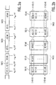
    1. A method of interleaving a digital signal in which samples are delayed an integral number of times a unit delay (ΔT) in accordance with a cyclically repeated delay pattern (a1,..,aM), characterized in that said method comprises the following steps:
      cyclically activating parallel-arranged select lines (AL(1)..AL(M)) of a memory (MEM) at a cycle rate which is equal to unit delay (ΔT);
      writing data (IG(1,j)..IG(k,j)) during an activation of a select line, which data comprises a relevant bit of each sample to be delayed in an integral number of sample groups, a sample group being associated with one delay pattern cycle;
      reading data ((b(1,1,j)@a1..b(1,M,j)@aM..b(k,1,j)@a1..b(k,M,j)@aM) during the activation of said select line, which data comprises a number of bits equal to the number of bits which is written, said bits being read in accordance with the delay pattern.
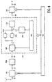
    2. An interleaving arrangement for interleaving a digital signal in which samples are delayed an integral number of times a unit delay (ΔT) in accordance with a cyclically repeated delay pattern (1a1,..,aM), characterized in that said interleaving arrangement comprises:
      means (HAS) for cyclically activating parallel-arranged select lines (AL(1)..AL(M)) of a memory (MEM) at a cycle rate which is equal to unit delay (ΔT);
      means (HAS) for writing data (IG(1,j)..IG(k,j)) during an activation of a select line, which data comprises a relevant bit of each sample to be delayed in an integral number of sample groups, a sample group being associated with one delay pattern cycle;
      means (HAS) for reading data
      (b(1,1,j)@a1..b(1,M,j)@aM..b(k,1,j)@a1..b(k,M,j)@aM) during the activation of said select line, which data comprises a number of bits which is equal to the number of bits written, said bits being read in accordance with the delay pattern.
    3. A receiver comprising the interleaving arrangement of claim 2, wherein said bits being read are in accordance with a delay pattern complementary to said delay pattern (a1,...,aM).
    4. A transmitter comprising the interleaving arrangement of claim 2.
    EP95937991A 1994-12-23 1995-12-04 Interleaving with low-speed memory Expired - Lifetime EP0748538B1 (en)

    Priority Applications (1)

    Application Number Priority Date Filing Date Title
    EP95937991A EP0748538B1 (en) 1994-12-23 1995-12-04 Interleaving with low-speed memory

    Applications Claiming Priority (4)

    Application Number Priority Date Filing Date Title
    EP94203745 1994-12-23
    EP94203745 1994-12-23
    EP95937991A EP0748538B1 (en) 1994-12-23 1995-12-04 Interleaving with low-speed memory
    PCT/IB1995/001088 WO1996020536A1 (en) 1994-12-23 1995-12-04 Interleaving with low-speed memory

    Publications (2)

    Publication Number Publication Date
    EP0748538A1 EP0748538A1 (en) 1996-12-18
    EP0748538B1 true EP0748538B1 (en) 2002-04-10

    Family

    ID=8217485

    Family Applications (1)

    Application Number Title Priority Date Filing Date
    EP95937991A Expired - Lifetime EP0748538B1 (en) 1994-12-23 1995-12-04 Interleaving with low-speed memory

    Country Status (6)

    Country Link
    US (1) US6424680B1 (en)
    EP (1) EP0748538B1 (en)
    JP (1) JP3610069B2 (en)
    KR (1) KR100427521B1 (en)
    DE (1) DE69526337T2 (en)
    WO (1) WO1996020536A1 (en)

    Families Citing this family (9)

    * Cited by examiner, † Cited by third party
    Publication number Priority date Publication date Assignee Title
    US5828671A (en) * 1996-04-10 1998-10-27 Motorola, Inc. Method and apparatus for deinterleaving an interleaved data stream
    DE69721495T2 (en) * 1996-11-11 2004-03-18 Koninklijke Philips Electronics N.V. RECEIVER, DE-STACKING AGENT AND METHOD FOR MEMORY DE-STACKING IN A SHORT TIME
    JP3697833B2 (en) * 1997-04-23 2005-09-21 ソニー株式会社 Broadcast signal receiver
    JP2958308B1 (en) 1998-07-10 1999-10-06 松下電器産業株式会社 De-interleaving device
    DE19936272C2 (en) * 1999-07-31 2001-09-27 Bosch Gmbh Robert Device for receiving digital signals and device for sending digital signals
    KR100601624B1 (en) * 1999-10-30 2006-07-14 삼성전자주식회사 Apparatus and method for interleaving and deinterleaving
    US20050180332A1 (en) * 2004-02-13 2005-08-18 Broadcom Corporation Low latency interleaving and deinterleaving
    EP1607879A1 (en) * 2004-06-14 2005-12-21 Dialog Semiconductor GmbH Memory interleaving in a computer system
    KR101491643B1 (en) 2013-09-23 2015-02-09 (주)에프씨아이 Diversity Receiver

    Family Cites Families (6)

    * Cited by examiner, † Cited by third party
    Publication number Priority date Publication date Assignee Title
    US4516219A (en) * 1981-12-18 1985-05-07 Mitsubishi Denki Kabushiki Kaisha Address designating method of memory and apparatus therefor
    US4907215A (en) * 1986-08-27 1990-03-06 Sony Corporation Integral optical recording of product code in data areas
    US5063533A (en) * 1989-04-10 1991-11-05 Motorola, Inc. Reconfigurable deinterleaver/interleaver for block oriented data
    NL8901631A (en) 1989-06-28 1991-01-16 Philips Nv Device for buffering data for the duration of cyclically repetitive buffering times.
    US5483541A (en) * 1993-09-13 1996-01-09 Trw Inc. Permuted interleaver
    US5592492A (en) * 1994-05-13 1997-01-07 Lsi Logic Corporation Convolutional interleaving/de-interleaving method and apparatus for data transmission

    Also Published As

    Publication number Publication date
    EP0748538A1 (en) 1996-12-18
    JPH09509818A (en) 1997-09-30
    JP3610069B2 (en) 2005-01-12
    DE69526337T2 (en) 2002-12-05
    DE69526337D1 (en) 2002-05-16
    KR970701458A (en) 1997-03-17
    US6424680B1 (en) 2002-07-23
    WO1996020536A1 (en) 1996-07-04
    KR100427521B1 (en) 2004-07-16

    Similar Documents

    Publication Publication Date Title
    US8127199B2 (en) SDRAM convolutional interleaver with two paths
    KR100362090B1 (en) Convolutional Interleaver and Deinterleaver, and Address Generator
    EP0748538B1 (en) Interleaving with low-speed memory
    EP1253729B1 (en) Reducing scintillation effects for optical free-space transmission
    TWI493973B (en) Digital video demodulation apparatus and associated method
    KR100754077B1 (en) Interleaver and method for interleaving an input data bit sequence using a coded storing of symbol and additional information
    JP3239084B2 (en) Multicarrier transmission interleaving apparatus and method
    US6598198B1 (en) Deinterleaving device that releases a plurality of types of interleaving simultaneously
    US6058118A (en) Method for the dynamic reconfiguration of a time-interleaved signal, with corresponding receiver and signal
    EP2242265B1 (en) A wireless communication receiver, a wireless communication receiving method and a television receiver
    US6192493B1 (en) Data element interleaving/deinterleaving
    JP3804989B2 (en) Receiver, deinterleave means and method for reduced time deinterleave memory
    JP3117706B2 (en) Data interleaving method and circuit
    US7886203B2 (en) Method and apparatus for bit interleaving and deinterleaving in wireless communication systems
    GB2456292A (en) Interleaver which reads out and writes into the nth memory address of the previous frames read/write address sequence for each successive frame
    JPH11127083A (en) Convolution interleaver and interleaver processing method
    JP3865743B2 (en) Digital broadcast receiving apparatus and digital broadcast receiving method
    EP1089440A1 (en) Interleaver and method for interleaving a data bit sequence
    JP3103098B2 (en) PCM audio decoder
    KR100710223B1 (en) Memory control system and the method of sending/receiving data using the system
    CN101500099B (en) Wireless communication receiver, wireless communication receiving method and television receiver
    JPH05284540A (en) Encoder and decoder
    CA2208475C (en) Method for the dynamic reconfiguration of a time-interleaved signal, with corresponding receiver and signal
    JPH01280984A (en) Satellite data broadcast signal receiver
    KR20070058758A (en) Time de-interleaving device and method

    Legal Events

    Date Code Title Description
    PUAI Public reference made under article 153(3) epc to a published international application that has entered the european phase

    Free format text: ORIGINAL CODE: 0009012

    AK Designated contracting states

    Kind code of ref document: A1

    Designated state(s): DE FR GB IT

    17P Request for examination filed

    Effective date: 19970107

    17Q First examination report despatched

    Effective date: 20000211

    GRAG Despatch of communication of intention to grant

    Free format text: ORIGINAL CODE: EPIDOS AGRA

    GRAG Despatch of communication of intention to grant

    Free format text: ORIGINAL CODE: EPIDOS AGRA

    GRAH Despatch of communication of intention to grant a patent

    Free format text: ORIGINAL CODE: EPIDOS IGRA

    GRAH Despatch of communication of intention to grant a patent

    Free format text: ORIGINAL CODE: EPIDOS IGRA

    REG Reference to a national code

    Ref country code: GB

    Ref legal event code: IF02

    GRAA (expected) grant

    Free format text: ORIGINAL CODE: 0009210

    AK Designated contracting states

    Kind code of ref document: B1

    Designated state(s): DE FR GB IT

    PG25 Lapsed in a contracting state [announced via postgrant information from national office to epo]

    Ref country code: IT

    Free format text: LAPSE BECAUSE OF FAILURE TO SUBMIT A TRANSLATION OF THE DESCRIPTION OR TO PAY THE FEE WITHIN THE PRESCRIBED TIME-LIMIT;WARNING: LAPSES OF ITALIAN PATENTS WITH EFFECTIVE DATE BEFORE 2007 MAY HAVE OCCURRED AT ANY TIME BEFORE 2007. THE CORRECT EFFECTIVE DATE MAY BE DIFFERENT FROM THE ONE RECORDED.

    Effective date: 20020410

    RIC1 Information provided on ipc code assigned before grant

    Free format text: 7H 03M 13/27 A, 7G 11B 20/18 B

    REF Corresponds to:

    Ref document number: 69526337

    Country of ref document: DE

    Date of ref document: 20020516

    ET Fr: translation filed
    ET Fr: translation filed
    REG Reference to a national code

    Ref country code: GB

    Ref legal event code: 746

    Effective date: 20020918

    REG Reference to a national code

    Ref country code: FR

    Ref legal event code: D6

    PLBE No opposition filed within time limit

    Free format text: ORIGINAL CODE: 0009261

    STAA Information on the status of an ep patent application or granted ep patent

    Free format text: STATUS: NO OPPOSITION FILED WITHIN TIME LIMIT

    26N No opposition filed

    Effective date: 20030113

    PGFP Annual fee paid to national office [announced via postgrant information from national office to epo]

    Ref country code: GB

    Payment date: 20041222

    Year of fee payment: 10

    PGFP Annual fee paid to national office [announced via postgrant information from national office to epo]

    Ref country code: FR

    Payment date: 20041228

    Year of fee payment: 10

    PGFP Annual fee paid to national office [announced via postgrant information from national office to epo]

    Ref country code: DE

    Payment date: 20050215

    Year of fee payment: 10

    PG25 Lapsed in a contracting state [announced via postgrant information from national office to epo]

    Ref country code: GB

    Free format text: LAPSE BECAUSE OF NON-PAYMENT OF DUE FEES

    Effective date: 20051204

    PG25 Lapsed in a contracting state [announced via postgrant information from national office to epo]

    Ref country code: DE

    Free format text: LAPSE BECAUSE OF NON-PAYMENT OF DUE FEES

    Effective date: 20060701

    GBPC Gb: european patent ceased through non-payment of renewal fee

    Effective date: 20051204

    PG25 Lapsed in a contracting state [announced via postgrant information from national office to epo]

    Ref country code: FR

    Free format text: LAPSE BECAUSE OF NON-PAYMENT OF DUE FEES

    Effective date: 20060831

    REG Reference to a national code

    Ref country code: FR

    Ref legal event code: ST

    Effective date: 20060831