EP0747802A2 - Système hiérarchique de répartition d'horloge et méthode - Google Patents
Système hiérarchique de répartition d'horloge et méthode Download PDFInfo
- Publication number
- EP0747802A2 EP0747802A2 EP96304145A EP96304145A EP0747802A2 EP 0747802 A2 EP0747802 A2 EP 0747802A2 EP 96304145 A EP96304145 A EP 96304145A EP 96304145 A EP96304145 A EP 96304145A EP 0747802 A2 EP0747802 A2 EP 0747802A2
- Authority
- EP
- European Patent Office
- Prior art keywords
- clock
- delay
- blocks
- sub
- elements
- Prior art date
- Legal status (The legal status is an assumption and is not a legal conclusion. Google has not performed a legal analysis and makes no representation as to the accuracy of the status listed.)
- Withdrawn
Links
Images


Classifications
-
- G—PHYSICS
- G06—COMPUTING; CALCULATING OR COUNTING
- G06F—ELECTRIC DIGITAL DATA PROCESSING
- G06F1/00—Details not covered by groups G06F3/00 - G06F13/00 and G06F21/00
- G06F1/04—Generating or distributing clock signals or signals derived directly therefrom
- G06F1/10—Distribution of clock signals, e.g. skew
-
- G—PHYSICS
- G06—COMPUTING; CALCULATING OR COUNTING
- G06F—ELECTRIC DIGITAL DATA PROCESSING
- G06F30/00—Computer-aided design [CAD]
- G06F30/30—Circuit design
- G06F30/39—Circuit design at the physical level
- G06F30/394—Routing
Definitions
- the present invention generally relates to the art of microelectronic integrated circuits, and more specifically to a hierarchial clock distribution system and method for optimally equalizing clock skew to circuitry in blocks of an integrated circuit.
- a large microelectronic integrated circuit such as an Application Specific Integrated Circuit (ASIC)
- ASIC Application Specific Integrated Circuit
- the circuitry is driven by clock pulses that are applied through an input clock driver and distributed via interconnect wiring to the various blocks of the circuit and other devices that are not included in the blocks.
- the clock pulses In order for the circuit to function properly, the clock pulses must arrive at each clocked circuit element at the same time. However, the lengths of the wiring that conduct the clock pulses to the different blocks will generally be different. Since the length of time required for an electrical signal to propagate through a wire is proportional to the length of the wire, the clock pulses will arrive at the blocks at different times.
- skew The phase or timing difference between the clock pulse arrival time to any two clocked circuit element in a microelectronic integrated circuit.
- This function can be provided by inserting delay buffers in the circuit having different delays to compensate for the different values of delay at the individual blocks.
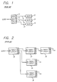
- Input clock pulses CLOCK are applied to a plurality of delay buffers 10, 12 and 14, which are connected through lines 16, 18 and 20 to circuit blocks 22, 24 and 26 respectively.
- the buffers 10, 12 and 14 delay the clock pulses by different lengths of time to compensate for the different lengths of the lines 16, 18 and 20 such that the clock pulses CLOCK arrive at the blocks 22, 24 and 26 simultaneously.
- the system comprises a plurality of fanout circuits 30, 32, 34, 36 and 38, each including an input delay buffer and a plurality of output delay buffers which are collectively designated by the reference character B. As illustrated, each fanout circuit has three outputs, although the actual number of outputs is not relevant.
- the output delay buffers B of the fanout circuit 30 are connected to the input delay buffers B of the fanout circuits 32, 34 and 36, which collectively produce nine outputs.
- Each output of the fanout circuits 32, 34 and 36 is connected to an input of another fanout circuit to provide a total of 27 outputs, and the hierarchial chain can continue to as many levels as desired. Only one fanout circuit 38 is illustrated as being connected to an output buffer B of the fanout circuit 32 for simplicity of illustration.
- the output buffers of the fanout circuits are connected to respective circuit blocks of a microelectronic integrated circuit, although not explicitly illustrated, in the manner described above with reference to FIG. 1.
- the skew from the clock input to the blocks can be equalized.
- the buffers B are implemented as programmable delay elements such as illustrated in FIG. 3.
- Each delay buffer B includes a chain of cascaded fixed delay elements 42, 44, 46 and 48 having outputs connected to inputs of a multiplexer 50.
- the delay at the output of each delay element is equal to the delay that itself produces plus the accumulated delay of the upstream delay elements.
- the output of the delay element 42 has a minimum delay value, whereas the output of the delay element 48 has a maximum delay value.
- the system comprises a phase locked loop or other type of phase comparator that compares reference clock pulses having the required skew with output pulses CLOCK' from the multiplexer 50 of each buffer B.
- the comparator then generates and applies a unique SELECT signal to the multiplexer 50 of each buffer B designating which multiplexer input (output of respective delay element 42, 44, 46 or 48) to pass therethrough as output pulses CLOCK'.
- the value of the SELECT signal corresponds to the delay required to make the phase or skew of the pulses CLOCK' coincide with that of the reference pulses.
- FIGs. 1 to 3 Although effective in equalizing the skew in an integrated circuit having a hierarchial block structure, the arrangement of FIGs. 1 to 3 is disadvantageous in that it requires programmable delay buffers and phase comparison circuitry. This undesirably increases the complexity and cost of the integrated circuit.
- a microelectronic circuit includes a plurality of circuitry blocks and sub-blocks, a clock driver, an electrical interconnect that directly connects the clock driver to the sub-blocks, and balanced clock-tree distribution systems provided between the electrical interconnect and circuitry in the sub-blocks respectively.
- a method of providing a hierarchial clock distribution system for the circuit includes determining clock delays between the clock driver and the clocked circuit elements within sub-blocks respectively.
- Delay buffers are selected from a predetermined set of fixed delay buffers having the same physical size and different delays, with the delay buffers being selected to provide equal clock delay between the clock driver and the distribution systems respectively.
- Each delay buffer includes a delay line, and a number of loading elements that are connected to the delay line, with the number of loading elements being selected to provide the required clock delay for the respective sub-block.
- FIG. 4 A hierarchial clock distribution system embodying the present invention is illustrated in FIG. 4 and generally designated by the reference numeral 60.
- the system 60 is implemented as part of a microelectronic integrated circuit 62 which typically receives clock pulses CLOCK from an external source. However, it is within the scope of the invention, although not explicitly illustrated, to provide a clock pulse generator as part of the circuit 62 itself.
- the clock pulses CLOCK are applied to a clock driver 64, which applies the clock pulses through an electrical interconnect wiring 66 to microelectronic circuit modules or blocks 68, 70 and 72.
- the block 72 comprises sub-blocks 72a, 72b and 72c.
- the wiring 66 is connected to a clock delay buffer B in each block 68 and 70, and in each sub-block 72a, 72b and 72c. It will be noted that no buffer B is provided in the block 72 between the wiring 66 and the sub-blocks 72a, 72b and 72c.
- FIG. 4 Although only two levels of hierarchy are illustrated in FIG. 4, consisting of one block level and one sub-block level, the invention is not so limited.
- a hierarchial structure including any number of block/sub-block levels can be provided in accordance with the present invention.
- a delay buffer B will be provided typically at the first and second hierarchial block level.
- the individual time delays provided by the delay buffers B are selected to equalize the clock delay between the driver 64 and clocked circuit elements or cells C in each block. Skew compensation within the blocks or sub-blocks 68, 70, 72a, 72b and 72c is provided by balanced clock tree distribution systems 74, 76, 78, 80 and 82 respectively.
- each balanced clock tree distribution system 74, 76, 78, 80 and 82 is shown as comprising the clocked circuitry elements or cells C, and local buffers or drivers D and E that are connected between the buffers B and the cells C.
- balanced clock tree distribution is performed by using a clock partition to split the original clock net into buffered sub-clock nets in a bottom-up fashion after placement of the cells C, without the local buffers D.
- An initial grouping of clocked cells C (cells having clock pins) is obtained according to the spread of the cells C and the distance among the neighboring clocked cells C. Then, the clocked cells C are exchanged among the groups to get the optimum result.
- the objective is to minimize both the maximum absolute loading difference among the groups and the standard deviation of the loading of the groups. After the grouping, an appropriate number of balance cells (not shown) are added to balance the loading for each group.
- each balance cell is calculated to balance the area and spread of the group with respect to other groups.
- the location of the local buffers D and E are calculated as the optimum balance center, based on the estimated routing pattern of the group to minimize the skew among the clocked cells C.
- all the balance cells and buffers D and E are inserted into the design and placed automatically in layout, based on the calculated coordinates.
- the present invention enables effective clock skew compensation using fixed delay buffers B, which is difficult to obtain using the prior art arrangements illustrated in FIGs. 1, 2 and 3.
- the invention accomplishes this goal by providing the delay buffers B only at one sub-block level, thereby eliminating accumulated hierarchial delay inaccuracies, and performing block level skew compensation using the balanced clock tree distribution systems.
- each delay buffer B has the same physical size in order to facilitate placement in the circuit 62.
- Each buffer B comprises the same number, here illustrated as four, of logic elements which provide known delays.
- the logic elements are inverters 90, 92, 94 and 96, although the invention is not so limited.
- the inverters can be replaced by, for example, NOR gates or wire delay lines, although not explicitly illustrated.
- the inverters 90, 92, 94 and 96 are connected in a cascade or chain, such that the clock pulses CLOCK' are delayed by the sum of the delays provided by the individual inverters 90, 92, 94 and 96.
- each inverter provides a delay of 0.25 ns, such that the total delay provided by the inverters 90, 92, 94 and 96 alone is 1.0 ns.
- Each delay buffer B is capable of providing a delay ranging from 1.0 ns to, for example 3.0 ns, by variably loading the outputs of the inverters 90, 92, 94 and 96 using loading elements 98.
- Each loading element 98 comprises, in the illustrated example, a PMOS field-effect transistor 98a and/or an NMOS field-effect transistor 98b that have their gates connected to the output of the respective inverter.
- the source and drain of each transistor 98a is connected to a first constant electrical potential source VDD, whereas the source and drain of each transistor 98b are connected to a second constant electrical potential source which is illustrated as being ground.
- Each loading element 98 causes the delay of the respective inverter 90, 92, 94 and 96 to be increased by, for example, 0.1 ns.
- loading elements 98 are first provided at the output of the first inverter 90. If more loading elements 98 are required, they are provided at the outputs of the inverters 92, 94 and 96 in consecutive order.
- the design of the integrated circuit 62 is facilitated by providing a circuit library set of 20 delay buffers 98 which differ from each other only in that they have 20 different numbers of loading elements 98 to provide the 20 different values of delay respectively.
- a timing analysis is performed on the circuit 62 to determine the value of delay between the clock driver 64 and each clocked cell C. This is accomplished by assigning initially a minimum delay value (1.0 ns) to each delay buffer B, and determining the delay at the input pin of clocked cell C.
- the timing analysis can be advantageously performed using, for example, the Timing Analyzer Release 2.2 which is commercially available as part of the Concurrent MDE® Design System (C-MDE® Design System) from LSI Logic Corporation of Milpitas, CA.
- the value of delay which the buffer B is required to produce in order to equalize the delay at the inputs of all of the clocked cells C is calculated, and one of the 20 possible buffer configurations is selected from the library set which has the corresponding value of delay.
- the buffers B are then inserted into the design and placed automatically in layout, based on the required delay values.
- the numbers of delay elements and loading elements in the buffers B as described above, as well as the specific delays that they provide, are exemplary only, and can be varied in any manner to accommodate a particular application.
Applications Claiming Priority (2)
| Application Number | Priority Date | Filing Date | Title |
|---|---|---|---|
| US482763 | 1995-06-07 | ||
| US08/482,763 US5570045A (en) | 1995-06-07 | 1995-06-07 | Hierarchical clock distribution system and method |
Publications (2)
| Publication Number | Publication Date |
|---|---|
| EP0747802A2 true EP0747802A2 (fr) | 1996-12-11 |
| EP0747802A3 EP0747802A3 (fr) | 1997-07-09 |
Family
ID=23917364
Family Applications (1)
| Application Number | Title | Priority Date | Filing Date |
|---|---|---|---|
| EP96304145A Withdrawn EP0747802A3 (fr) | 1995-06-07 | 1996-06-05 | Système hiérarchique de répartition d'horloge et méthode |
Country Status (3)
| Country | Link |
|---|---|
| US (2) | US5570045A (fr) |
| EP (1) | EP0747802A3 (fr) |
| JP (1) | JPH096463A (fr) |
Families Citing this family (71)
| Publication number | Priority date | Publication date | Assignee | Title |
|---|---|---|---|---|
| US5655149A (en) * | 1994-06-10 | 1997-08-05 | Harris Corporation | System for identifying a primary processor and non-primary processors after system reboot independent of processor positions and without using default primary processor identification |
| US5570045A (en) * | 1995-06-07 | 1996-10-29 | Lsi Logic Corporation | Hierarchical clock distribution system and method |
| US5717229A (en) * | 1996-03-26 | 1998-02-10 | Intel Corporation | Method and apparatus for routing a clock tree in an integrated circuit package |
| US6124744A (en) * | 1996-03-26 | 2000-09-26 | Kabushiki Kaisha Toshiba | Electronic circuit apparatus having circuits for effectively compensating for clock skew |
| US5880607A (en) * | 1996-05-01 | 1999-03-09 | Sun Microsystems, Inc. | Clock distribution network with modular buffers |
| US6157237A (en) * | 1996-05-01 | 2000-12-05 | Sun Microsystems, Inc. | Reduced skew control block clock distribution network |
| US5850150A (en) * | 1996-05-01 | 1998-12-15 | Sun Microsystems, Inc. | Final stage clock buffer in a clock distribution network |
| US6014510A (en) * | 1996-11-27 | 2000-01-11 | International Business Machines Corporation | Method for performing timing analysis of a clock circuit |
| US6185723B1 (en) * | 1996-11-27 | 2001-02-06 | International Business Machines Corporation | Method for performing timing analysis of a clock-shaping circuit |
| US5861764A (en) * | 1996-12-31 | 1999-01-19 | Compaq Computer Corporation | Clock skew reduction using spider clock trace routing |
| US6144224A (en) * | 1997-06-16 | 2000-11-07 | International Business Machines Corporation | Clock distribution network with dual wire routing |
| KR100291185B1 (ko) * | 1997-06-26 | 2001-07-12 | 박종섭 | 클럭 스큐를 최소화하는 장치 |
| KR100247477B1 (ko) * | 1997-06-30 | 2000-03-15 | 김영환 | 비중복 2위상 클럭 간의 스큐 조절을 위한 클럭 장치 |
| JP3022426B2 (ja) * | 1997-08-14 | 2000-03-21 | 日本電気株式会社 | クロック信号供給用集積回路及びその構成方法 |
| JP3566051B2 (ja) * | 1997-11-14 | 2004-09-15 | 株式会社ルネサステクノロジ | 位相の異なる複数のクロック信号を出力するクロック信号発生回路およびそれを用いたクロック位相制御回路 |
| US6067648A (en) * | 1998-03-02 | 2000-05-23 | Tanisys Technology, Inc. | Programmable pulse generator |
| EP0953892A1 (fr) * | 1998-04-29 | 1999-11-03 | Lsi Logic Corporation | Procédé pour la distribution de signaux d'horloge à des circuits de charge dans un dispositif ASIC |
| JPH11316617A (ja) | 1998-05-01 | 1999-11-16 | Mitsubishi Electric Corp | 半導体回路装置 |
| US6192092B1 (en) * | 1998-06-15 | 2001-02-20 | Intel Corp. | Method and apparatus for clock skew compensation |
| US6305001B1 (en) * | 1998-06-18 | 2001-10-16 | Lsi Logic Corporation | Clock distribution network planning and method therefor |
| FR2781065B1 (fr) * | 1998-07-10 | 2000-08-25 | St Microelectronics Sa | Procede de placement-routage d'un circuit d'horloge globale sur un circuit integre, et dispositifs associes |
| JP3753355B2 (ja) * | 1998-11-10 | 2006-03-08 | 株式会社ルネサステクノロジ | 半導体装置 |
| US6472922B1 (en) * | 1999-01-14 | 2002-10-29 | Sony Corporation | System and method for flexibly distributing timing signals |
| US6321342B1 (en) | 1999-03-23 | 2001-11-20 | Lsi Logic Corporation | Method and apparatus for interfacing circuits that operate based upon different clock signals |
| GB2348753B (en) * | 1999-03-27 | 2003-07-23 | Evan Arkas | Pulse clock/signal delay apparatus & method |
| US6367060B1 (en) * | 1999-06-18 | 2002-04-02 | C. K. Cheng | Method and apparatus for clock tree solution synthesis based on design constraints |
| DE60045383D1 (de) | 1999-08-16 | 2011-01-27 | Japan Science & Tech Agency | Optische supraleitende anordnung |
| JP2001125937A (ja) * | 1999-10-25 | 2001-05-11 | Fujitsu Ltd | 半導体集積回路装置のレイアウト設計システム、半導体集積回路装置のレイアウト設計方法、およびそのシステムにおける各手段をもしくはその方法における各工程をコンピュータに実行させるプログラムを記録したコンピュータ読み取り可能な記録媒体 |
| US6513149B1 (en) | 2000-03-31 | 2003-01-28 | International Business Machines Corporation | Routing balanced clock signals |
| JP2002041591A (ja) * | 2000-07-28 | 2002-02-08 | Mitsubishi Electric Corp | クロック分配回路の配置配線方法、クロック分配回路の製造方法、半導体装置の製造方法、クロック分配回路、および半導体装置 |
| US6573757B1 (en) * | 2000-09-11 | 2003-06-03 | Cypress Semiconductor Corp. | Signal line matching technique for ICS/PCBS |
| GB2370380B (en) | 2000-12-19 | 2003-12-31 | Picochip Designs Ltd | Processor architecture |
| TW494293B (en) * | 2000-12-22 | 2002-07-11 | Faraday Tech Corp | Clock signal network structure |
| US6909127B2 (en) * | 2001-06-27 | 2005-06-21 | Intel Corporation | Low loss interconnect structure for use in microelectronic circuits |
| US6522186B2 (en) * | 2001-06-27 | 2003-02-18 | Intel Corporation | Hierarchical clock grid for on-die salphasic clocking |
| US6925555B2 (en) * | 2001-07-27 | 2005-08-02 | Hewlett-Packard Development Company, L.P. | System and method for determining a plurality of clock delay values using an optimization algorithm |
| JP3672889B2 (ja) * | 2001-08-29 | 2005-07-20 | Necエレクトロニクス株式会社 | 半導体集積回路とそのレイアウト方法 |
| US6957358B1 (en) | 2002-01-28 | 2005-10-18 | Cisco Systems, Inc. | Scaling dynamic clock distribution for large service provider networks |
| US7158925B2 (en) * | 2002-04-18 | 2007-01-02 | International Business Machines Corporation | Facilitating simulation of a model within a distributed environment |
| JP3767520B2 (ja) * | 2002-06-12 | 2006-04-19 | 日本電気株式会社 | 集積回路装置 |
| US7043599B1 (en) | 2002-06-20 | 2006-05-09 | Rambus Inc. | Dynamic memory supporting simultaneous refresh and data-access transactions |
| US6873187B1 (en) * | 2002-10-29 | 2005-03-29 | Lattice Semiconductor Corporation | Method and apparatus for controlling signal distribution in an electronic circuit |
| US7124314B2 (en) * | 2002-11-05 | 2006-10-17 | Ip-First, Llc | Method and apparatus for fine tuning clock signals of an integrated circuit |
| US7073145B2 (en) * | 2003-01-07 | 2006-07-04 | International Business Machines Corporation | Programmable delay method for hierarchical signal balancing |
| US6986116B2 (en) * | 2003-01-07 | 2006-01-10 | International Business Machines Corporation | Signal balancing between voltage domains |
| GB2397668B (en) * | 2003-01-27 | 2005-12-07 | Picochip Designs Ltd | Processor array |
| JP2004253772A (ja) * | 2003-01-31 | 2004-09-09 | Matsushita Electric Ind Co Ltd | 半導体集積回路装置 |
| US7256633B1 (en) | 2003-05-01 | 2007-08-14 | Ample Communications, Inc. | Systems for implementing high speed and high integration chips |
| US20060044016A1 (en) * | 2004-08-24 | 2006-03-02 | Gasper Martin J Jr | Integrated circuit with signal skew adjusting cell selected from cell library |
| US6861884B1 (en) * | 2003-08-04 | 2005-03-01 | Rambus Inc. | Phase synchronization for wide area integrated circuits |
| US7017132B2 (en) * | 2003-11-12 | 2006-03-21 | Taiwan Semiconductor Manufacturing Company | Methodology to optimize hierarchical clock skew by clock delay compensation |
| US7903777B1 (en) | 2004-03-03 | 2011-03-08 | Marvell International Ltd. | System and method for reducing electromagnetic interference and ground bounce in an information communication system by controlling phase of clock signals among a plurality of information communication devices |
| WO2007052091A1 (fr) * | 2005-11-02 | 2007-05-10 | Freescale Semiconductor, Inc. | Procede et systeme permettant de reduire l'obliquite d'horloges dans des arbres d'horloges |
| US7586355B2 (en) * | 2007-07-11 | 2009-09-08 | United Memories, Inc. | Low skew clock distribution tree |
| GB2454865B (en) | 2007-11-05 | 2012-06-13 | Picochip Designs Ltd | Power control |
| GB2470037B (en) | 2009-05-07 | 2013-07-10 | Picochip Designs Ltd | Methods and devices for reducing interference in an uplink |
| GB2470771B (en) | 2009-06-05 | 2012-07-18 | Picochip Designs Ltd | A method and device in a communication network |
| GB2470891B (en) | 2009-06-05 | 2013-11-27 | Picochip Designs Ltd | A method and device in a communication network |
| GB2474071B (en) | 2009-10-05 | 2013-08-07 | Picochip Designs Ltd | Femtocell base station |
| US20110320997A1 (en) * | 2010-06-24 | 2011-12-29 | Lsi Corporation | Delay-Cell Footprint-Compatible Buffers |
| GB2482869B (en) | 2010-08-16 | 2013-11-06 | Picochip Designs Ltd | Femtocell access control |
| US8356264B2 (en) | 2010-10-28 | 2013-01-15 | International Business Machines Corporation | Implementing enhanced clock tree distributions to decouple across N-level hierarchical entities |
| GB2489919B (en) | 2011-04-05 | 2018-02-14 | Intel Corp | Filter |
| GB2489716B (en) | 2011-04-05 | 2015-06-24 | Intel Corp | Multimode base system |
| GB2491098B (en) | 2011-05-16 | 2015-05-20 | Intel Corp | Accessing a base station |
| US20140312928A1 (en) * | 2013-04-19 | 2014-10-23 | Kool Chip, Inc. | High-Speed Current Steering Logic Output Buffer |
| US9825755B2 (en) * | 2013-08-30 | 2017-11-21 | Qualcomm Incorporated | Configurable clock tree |
| TWI561958B (en) * | 2014-05-22 | 2016-12-11 | Global Unichip Corp | Integrated circuit |
| US9350339B2 (en) | 2014-07-18 | 2016-05-24 | Qualcomm Incorporated | Systems and methods for clock distribution in a die-to-die interface |
| DE102017127276A1 (de) * | 2017-08-30 | 2019-02-28 | Taiwan Semiconductor Manufacturing Co., Ltd. | Standardzellen und abwandlungen davon innerhalb einer standardzellenbibliothek |
| US10616103B2 (en) | 2017-12-01 | 2020-04-07 | International Business Machines Corporation | Constructing staging trees in hierarchical circuit designs |
Citations (2)
| Publication number | Priority date | Publication date | Assignee | Title |
|---|---|---|---|---|
| WO1987004306A1 (fr) * | 1985-12-30 | 1987-07-16 | Eta Systems, Inc. | Systeme d'accord d'horloge electronique |
| EP0552625A2 (fr) * | 1992-01-23 | 1993-07-28 | Motorola, Inc. | Mémoire avec compensation de variations de tension, de température et de fabrication |
Family Cites Families (18)
| Publication number | Priority date | Publication date | Assignee | Title |
|---|---|---|---|---|
| US3104330A (en) * | 1960-02-11 | 1963-09-17 | Gen Electric | Clock pulse distribution system for synchronously driving a plurality of flip-flops |
| US4769558A (en) * | 1986-07-09 | 1988-09-06 | Eta Systems, Inc. | Integrated circuit clock bus layout delay system |
| JPH083773B2 (ja) * | 1987-02-23 | 1996-01-17 | 株式会社日立製作所 | 大規模半導体論理回路 |
| US5239215A (en) * | 1988-05-16 | 1993-08-24 | Matsushita Electric Industrial Co., Ltd. | Large scale integrated circuit configured to eliminate clock signal skew effects |
| US4926066A (en) * | 1988-09-12 | 1990-05-15 | Motorola Inc. | Clock distribution circuit having minimal skew |
| US4912340A (en) * | 1988-10-21 | 1990-03-27 | Northern Telecom | Circuit for generating non-overlapping two-phase clocks |
| JPH0824143B2 (ja) * | 1989-02-08 | 1996-03-06 | 株式会社東芝 | 集積回路の配置配線方式 |
| US5254955A (en) * | 1989-08-25 | 1993-10-19 | Anritsu Corporation | Advanced phase locked loop circuit |
| JP2756325B2 (ja) * | 1989-12-07 | 1998-05-25 | 株式会社日立製作所 | クロック供給回路 |
| US5258660A (en) * | 1990-01-16 | 1993-11-02 | Cray Research, Inc. | Skew-compensated clock distribution system |
| US5206861A (en) * | 1990-08-28 | 1993-04-27 | International Business Machines Corporation | System timing analysis by self-timing logic and clock paths |
| US5204559A (en) * | 1991-01-23 | 1993-04-20 | Vitesse Semiconductor Corporation | Method and apparatus for controlling clock skew |
| US5109168A (en) * | 1991-02-27 | 1992-04-28 | Sun Microsystems, Inc. | Method and apparatus for the design and optimization of a balanced tree for clock distribution in computer integrated circuits |
| US5272390A (en) * | 1991-09-23 | 1993-12-21 | Digital Equipment Corporation | Method and apparatus for clock skew reduction through absolute delay regulation |
| US5278466A (en) * | 1991-09-27 | 1994-01-11 | Mitsubishi Denki Kabushiki Kaisha | Integrated circuit with reduced clock skew |
| US5307381A (en) * | 1991-12-27 | 1994-04-26 | Intel Corporation | Skew-free clock signal distribution network in a microprocessor |
| US5430397A (en) * | 1993-01-27 | 1995-07-04 | Hitachi, Ltd. | Intra-LSI clock distribution circuit |
| US5570045A (en) * | 1995-06-07 | 1996-10-29 | Lsi Logic Corporation | Hierarchical clock distribution system and method |
-
1995
- 1995-06-07 US US08/482,763 patent/US5570045A/en not_active Expired - Lifetime
-
1996
- 1996-06-05 EP EP96304145A patent/EP0747802A3/fr not_active Withdrawn
- 1996-06-07 JP JP8145513A patent/JPH096463A/ja active Pending
- 1996-08-28 US US08/704,831 patent/US5686845A/en not_active Expired - Lifetime
Patent Citations (2)
| Publication number | Priority date | Publication date | Assignee | Title |
|---|---|---|---|---|
| WO1987004306A1 (fr) * | 1985-12-30 | 1987-07-16 | Eta Systems, Inc. | Systeme d'accord d'horloge electronique |
| EP0552625A2 (fr) * | 1992-01-23 | 1993-07-28 | Motorola, Inc. | Mémoire avec compensation de variations de tension, de température et de fabrication |
Non-Patent Citations (3)
| Title |
|---|
| IEEE TRANSACTIONS ON COMPUTER AIDED DESIGN OF INTEGRATED CIRCUITS AND SYSTEMS, vol. 12, no. 2, 1 February 1993, pages 242-249, XP000386012 REN-SONG TSAY: "AN EXACT ZERO-SKEW CLOCK ROUTING ALGORITHM" * |
| LIN S ET AL: "PROCESS-VARIATION-TOLERANT CLOCK SKEW MINIMIZATION" 6 November 1994 , IEEE/ACM INTERNATIONAL CONFERENCE ON COMPUTER-AIDED DESIGN. DIGEST TECHNICAL PAPERS (ICCAD), SAN JOSE, NOV. 6 - 10, 1994, PAGE(S) 284 - 288 , INSTITUTE OF ELECTRICAL AND ELECTRONICS ENGINEERS XP000529838 * page 287, left-hand column, paragraph 1 - right-hand column, paragraph 1 * * |
| PROCEEDINGS OF THE ANNUAL IEEE INTERNATIONAL ASIC CONFERENCE AND EXHIBIT, September 1992, ROCHESTER NY, pages 26-29, XP000670854 ERDAL A. ET AL: "AN IMPLEMENTATION OF A CLOCK-TREE DISTRIBUTION SCHEME FOR HIGH-PERFORMANCE ASICS" * |
Also Published As
| Publication number | Publication date |
|---|---|
| US5686845A (en) | 1997-11-11 |
| EP0747802A3 (fr) | 1997-07-09 |
| US5570045A (en) | 1996-10-29 |
| JPH096463A (ja) | 1997-01-10 |
Similar Documents
| Publication | Publication Date | Title |
|---|---|---|
| US5570045A (en) | Hierarchical clock distribution system and method | |
| US5414381A (en) | Method of adjusting for clock skew | |
| US7017132B2 (en) | Methodology to optimize hierarchical clock skew by clock delay compensation | |
| US5339253A (en) | Method and apparatus for making a skew-controlled signal distribution network | |
| US6367060B1 (en) | Method and apparatus for clock tree solution synthesis based on design constraints | |
| US8115530B2 (en) | Robust time borrowing pulse latches | |
| US8887110B1 (en) | Methods for designing intergrated circuits with automatically synthesized clock distribution networks | |
| JPH08339236A (ja) | クロック信号分配回路 | |
| US7119596B2 (en) | Wide-range programmable delay line | |
| US7937604B2 (en) | Method for generating a skew schedule for a clock distribution network containing gating elements | |
| US6574781B1 (en) | Design methodology for inserting RAM clock delays | |
| JP4218924B2 (ja) | 半導体集積回路の設計システム | |
| US6763513B1 (en) | Clock tree synthesizer for balancing reconvergent and crossover clock trees | |
| JP2013179598A (ja) | 減少された挿入遅延を持つプログラマブル遅延回路 | |
| US7634748B2 (en) | Special engineering change order cells | |
| US8316334B2 (en) | Segment and bipartite graph based apparatus and method to address hold violations in static timing | |
| Chao et al. | Retiming and clock skew for synchronous systems | |
| US6075936A (en) | Logic circuit simulation apparatus having cycle-based simulator for simulating circuits including multi-cycle paths | |
| US6928572B2 (en) | Multistage clock delay circuit and method | |
| US20070273403A1 (en) | Clock Tree For Programmable Logic Array Devices | |
| US6757877B2 (en) | System and method for identifying and eliminating bottlenecks in integrated circuit designs | |
| US6275068B1 (en) | Programmable clock delay | |
| JPH08274260A (ja) | クロックスキュー低減方法 | |
| JPH11194848A (ja) | クロック遅延調整装置 | |
| JP3104746B2 (ja) | クロックツリーレイアウト装置 |
Legal Events
| Date | Code | Title | Description |
|---|---|---|---|
| PUAI | Public reference made under article 153(3) epc to a published international application that has entered the european phase |
Free format text: ORIGINAL CODE: 0009012 |
|
| AK | Designated contracting states |
Kind code of ref document: A2 Designated state(s): DE FR GB IT NL |
|
| PUAL | Search report despatched |
Free format text: ORIGINAL CODE: 0009013 |
|
| AK | Designated contracting states |
Kind code of ref document: A3 Designated state(s): DE FR GB IT NL |
|
| 17P | Request for examination filed |
Effective date: 19971023 |
|
| STAA | Information on the status of an ep patent application or granted ep patent |
Free format text: STATUS: THE APPLICATION IS DEEMED TO BE WITHDRAWN |
|
| 18D | Application deemed to be withdrawn |
Effective date: 20000104 |