EP0744238B1 - Bildanzeigeverfahren für eine flüssigkristallmaske-markiervorrichtung - Google Patents
Bildanzeigeverfahren für eine flüssigkristallmaske-markiervorrichtung Download PDFInfo
- Publication number
- EP0744238B1 EP0744238B1 EP95907837A EP95907837A EP0744238B1 EP 0744238 B1 EP0744238 B1 EP 0744238B1 EP 95907837 A EP95907837 A EP 95907837A EP 95907837 A EP95907837 A EP 95907837A EP 0744238 B1 EP0744238 B1 EP 0744238B1
- Authority
- EP
- European Patent Office
- Prior art keywords
- image
- liquid crystal
- picture elements
- crystal mask
- afterimage
- Prior art date
- Legal status (The legal status is an assumption and is not a legal conclusion. Google has not performed a legal analysis and makes no representation as to the accuracy of the status listed.)
- Expired - Lifetime
Links
- 239000004973 liquid crystal related substance Substances 0.000 title claims description 64
- 239000003550 marker Substances 0.000 title claims description 34
- 238000000034 method Methods 0.000 title claims description 29
- 230000001678 irradiating effect Effects 0.000 claims description 11
- 206010047571 Visual impairment Diseases 0.000 description 44
- 238000002834 transmittance Methods 0.000 description 17
- 230000005540 biological transmission Effects 0.000 description 2
- 239000007787 solid Substances 0.000 description 2
- 239000003990 capacitor Substances 0.000 description 1
- 238000010276 construction Methods 0.000 description 1
- 230000006866 deterioration Effects 0.000 description 1
- 230000002542 deteriorative effect Effects 0.000 description 1
- 238000010586 diagram Methods 0.000 description 1
- 230000000694 effects Effects 0.000 description 1
- 230000000630 rising effect Effects 0.000 description 1
- 230000001360 synchronised effect Effects 0.000 description 1
- 230000007704 transition Effects 0.000 description 1
- 238000011144 upstream manufacturing Methods 0.000 description 1
Images


Classifications
-
- B—PERFORMING OPERATIONS; TRANSPORTING
- B23—MACHINE TOOLS; METAL-WORKING NOT OTHERWISE PROVIDED FOR
- B23K—SOLDERING OR UNSOLDERING; WELDING; CLADDING OR PLATING BY SOLDERING OR WELDING; CUTTING BY APPLYING HEAT LOCALLY, e.g. FLAME CUTTING; WORKING BY LASER BEAM
- B23K26/00—Working by laser beam, e.g. welding, cutting or boring
- B23K26/02—Positioning or observing the workpiece, e.g. with respect to the point of impact; Aligning, aiming or focusing the laser beam
- B23K26/06—Shaping the laser beam, e.g. by masks or multi-focusing
- B23K26/064—Shaping the laser beam, e.g. by masks or multi-focusing by means of optical elements, e.g. lenses, mirrors or prisms
- B23K26/066—Shaping the laser beam, e.g. by masks or multi-focusing by means of optical elements, e.g. lenses, mirrors or prisms by using masks
Definitions
- the present invention relates to an image display method for a liquid crystal mask marker, and more particularly to an image display method for a liquid crystal mask marker which can clearly display and imprint mask images, such as the product numbers and patterns, on the surfaces of nonmetallic articles, such as IC chips, or metallic articles.
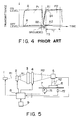
- a prior art liquid crystal mask marker will be described with reference to Fig. 5.
- a high-density energy light R1 emitted from a laser oscillator 1, for example, is irradiated to a display image of a liquid crystal mask 4, and a light R2 transmitted through the mask 4 is then irradiated to a workpiece surface 6 for imprinting the image on the workpiece surface 6.
- the display image of the liquid crystal mask 4 is rewritten with a controller 8 in such a manner that, as shown in Fig.
- FIGs. 7A to 7C for example, when a solid black circle A (Fig. 7A) is marked on the workpiece surface 6 and, after rewriting the display image of the liquid crystal mask 4, a solid black rectangle B (Fig. 7B) is marked on the workpiece surface 6, a rectangle C appears, together with an afterimage A2, as the image of the liquid crystal mask 4 immediately after the rewriting, as shown in Fig. 7C.
- the rectangle C is divided into a clear area A1 and an unclear area B1.
- This unclear area B1 is defined here as "counter afterimage”.
- the alphabet B indicates an area of the image other than the circle A.
- the afterimage A2 and the counter afterimage B1 will disappear naturally with the elapse of time. Therefore, those phenomena are practically not problematic in conventional liquid crystal mask markers which are much inferior in marking speed and image sharpness to the present liquid crystal mask marker described later. More specifically, in conventional liquid crystal mask markers, the high-density energy light R1 is irradiated to the image including both the afterimage A2 and the counter afterimage B1. But when the image is imprinted on the workpiece surface, the counter afterimage B1 does not raise a problem because the irradiation time is long. On the other hand, the afterimage A1 does not appear as imprinted on the workpiece surface by irradiating the high-density energy light R1 to the image in which the afterimage A2 has disappeared.
- the counter afterimage B1 will not also appear as imprinted on the workpiece surface if the high-density energy light R1 is, as with the above case of the afterimage A2, irradiated to the image in which the counter afterimage B1 has disappeared.
- the high-density energy light R1 is, as with the above case of the afterimage A2, irradiated to the image in which the counter afterimage B1 has disappeared.
- liquid crystal mask markers see, e.g., Japanese Patent Laid-Open No. 5-42379) wherein the rewriting time and the image display time are each on the order of about 30 msec at the minimum, i.e., an image is displayed and rewritten at very high speeds, while ensuring a sharpness of the image imprinted. Accordingly, the irradiation time of a high-density energy light (i.e., the marking time) during the image display time is even shorter.
- the present invention has been accomplished with a view of solving the above-stated problem in the prior art, and its object is to provide an image display method for a liquid crystal mask marker which can display an image of a higher sharpness at a higher speed with more reliability, taking into account the processing of an afterimage, the processing of a counter afterimage, and the irradiation timing of a high-density energy light.
- an image display method for a liquid crystal mask marker is featured as defined by claim 1.
- an image display method for a liquid crystal mask marker is featured as defined by claim 2.
- an image display method for a liquid crystal mask marker is featured as defined by claim 3.
- Fig. 4 which is an analytic graph for the prior art, the reference numerals in Figs. 7a to 7c are also employed. It is here assumed that a current image P1 comprising a transparent area A and an opaque area B is rewritten with the prior art process of grounding potentials of all the picture elements and the step of displaying a next image P2 is then started.
- the next image P2 has a transparent area comprising one portion A1 of the area A and one portion B1 of the area B, and an opaque area comprising the other portion A2 of the area A and the other portion B2 of the area B.
- Fig. 4 is a correlative graph between transmittance of each picture element in A, B, A1, A2, B1, B2 and time in the steps of displaying the current image P1, rewriting the image and displaying the current image P2.
- the graph of Fig. 4 also indicates the timing Ts to start irradiation of a high-density energy light and the irradiation time T.
- the sharpness of an image imprinted is represented by the product of the intensity of a light itself transmitted through each picture element and the transmission time "t" of the light.
- the afterimage A2 and the counter afterimage B1 are imprinted on the workpiece surface 6.
- the timing Ts to start the irradiation comes closer to the period of rewriting and, therefore, the sharpness of an image imprinted reduces more remarkably due to the occurrence of the afterimage A2 and the counter afterimage B1.
- FIG. 4 Another new problem can also be seen from Fig. 4. More specifically, when a liquid crystal mask marker is of the lump irradiating type, the afterimage A2 and the counter afterimage B1 occur uniformly. However, when a liquid crystal mask marker is of the raster irradiating type, the afterimage A2 and the counter afterimage B1 are more distinct in picture elements of the next image P2 on the side where the raster irradiation is started, than in picture elements thereof on the side where the raster irradiation is ended. Further, tendency analysis for the state of each picture element shows that if the picture element is in a stable state regardless of whether its past state was transparent or opaque, it takes a relatively long time to transit the picture element to the other state.
- the expression "are made transparent” means that both the picture elements A and B, i.e., all the picture elements, of the current image are turned once to a state transparent to the irradiated light.
- the voltage for only the picture elements B is raised to a value enough to make the picture elements B transparent.
- the expression “electrodes of all the picture elements are grounded” means that all the picture elements are processed in the same manner as the prior art process of grounding potentials of all the picture elements.
- the history of each picture element B in the current image P1 is cancelled, then electrodes of all the picture elements are grounded or set equipotential, and thereafter the step of displaying the next image P2 is started.
- the expression "are made opaque” means that both the picture elements A and B, i.e., all the picture elements, of the current image are turned once to a state opaque to the irradiated light.
- the voltage for only the picture elements A is lowered to a value enough to make the picture elements A opaque.
- the history of each of all the picture elements in the current image P1 is cancelled, then electrodes of all the picture elements are grounded or set equipotential, and thereafter the step of displaying the next image P2 is started.
- the expression "are reversed" means that the voltage for the picture elements A is lowered and the voltage for the picture elements B is raised. At this time, it is not necessarily required to turn the picture elements A from the transparent state to the completely opaque state and turn the picture elements B from the opaque state to the completely transparent state. It is essential that voltages are merely raised and lowered corresponding to the respective picture elements.
- the history of each of both the picture elements A and B in the current image P1 is cancelled, then electrodes of all the picture elements are grounded or set equipotential, and thereafter the step of displaying the next image P2 is started.
- Figs. 1 to 3 plot changes in transmittance of light through images and afterimages before and after rewriting of a display image as carried out according to the present invention, in which:
- Fig. 5 shows a liquid crystal mask marker employed in the first invention.
- a laser beam R1 emitted from a laser oscillator 1 is irradiated in a raster manner to the image surface of a liquid crystal mask 4 through a deflector 2 for raster irradiation.
- the term "raster irradiation" means that the thin laser beam R1 is irradiated while being moved successively in the X and Y directions.
- a laser beam R2 transmitted through the image surface of the liquid crystal mask 4 is then irradiated to a workpiece surface 6 through a deflector 5.
- the transmitted laser beam R2 contains information of a mask display image and this image is imprinted on the workpiece surface 6.
- the transmitted laser beam R2 is condensed toward the deflector 5 through the liquid crystal mask 4 by a condensing lens 3 placed upstream of the liquid crystal mask 4.
- one entire image P is divided into five images Pa to Pf beforehand and these divided images Pa to Pf are displayed by the liquid crystal mask 4 successively.
- the deflector 5 is operated whenever each image is displayed, so that the divided images Pa to Pf are imprinted in respective optimum areas of the workpiece surface 6.
- the marker system waits for a next workpiece (waiting time T2) and then repeats the above-explained marking operation on the next workpiece, as shown in Fig. 6A.
- the marker system includes a controller 8 which is electrically connected to the laser oscillator 1, the deflector 2 for raster irradiation, the liquid crystal mask 4, the deflector 5, a drive motor 71 for the workpiece feeder and a workpiece position sensor 72, and which controls these components in synchronous relation in accordance with commands from an external terminal 9.
- the controller 8 also instructs application of voltages to the liquid crystal mask 4 (i.e., applies voltages to the mask and makes it grounded), and adjustment of the applied voltages (i.e., raises and lowers the applied voltages).
- liquid crystal mask markers in which the present invention is employed are not necessarily limited to the liquid crystal mask marker of the raster irradiation type described above as an example.
- a liquid crystal mask marker of the lump irradiation type is obtained by replacing the deflector 2 for raster irradiation with a simple magnifying lens.
- the liquid crystal mask marker may be designed to imprint an entire image as a whole rather than dividing the entire image into a plurality images as explained above. In such a case, the procedures shown in Fig. 6B are not required.
- marking time T1" in Fig. 6A as "display” in Fig. 6B
- waiting time T2 in Fig. 6A as "grounded" plus “waiting time”.
- the control performed by the controller 8 is, for example, as follows.
- the construction, operation and advantages of the first embodiment will be described below with reference to Fig. 1 in which there is shown an analytic graph. Note that the reference numerals in Fig. 1 correspond to those in Fig. 4.
- the controller 8 outputs signals to the liquid crystal mask 4 to raise the voltage for the opaque picture elements B of the current image P1 once to a value enough to make the picture elements B transparent, then ground or set all the picture elements A and B equipotential, and thereafter start the step of displaying the next image P2.
- the afterimage A2 remains, but the counter afterimage B1 is eliminated, resulting in a higher sharpness of the image imprinted.
- transmittance values of the transparent areas A1 and B1 rise substantially at the same rate, the timing to irradiate the laser beam is easier to set and hence the marking speed can be increased with certainty.
- This second embodiment is different from the first embodiment in the display method for rewriting the display image.
- the controller 8 outputs signals to the liquid crystal mask 4 to lower the voltage for the transparent picture elements A of the current image P1 once to a value enough to make the picture elements A opaque, then ground or set all the picture elements A and B equipotential, and thereafter start the step of displaying the next image P2.
- the controller 8 outputs signals to the liquid crystal mask 4 to lower the voltage for the transparent picture elements A of the current image P1 once to a value enough to make the picture elements A opaque, then ground or set all the picture elements A and B equipotential, and thereafter start the step of displaying the next image P2.
- the controller 8 outputs signals to the liquid crystal mask 4 to lower the voltage for the transparent picture elements A of the current image P1 once to a value enough to make the picture elements A opaque, then ground or set all the picture elements A and B equipotential, and thereafter start the step of displaying the next image P2.
- all the picture elements A and B are grounded, after which the voltages for displaying the next image P2 are raised.
- the second embodiment thus constituted, as will be seen from the next image P2 in Fig. 2, the afterimage A2 and the counter afterimage B1 are both eliminated, resulting in a higher sharpness of the image imprinted.
- transmittance values of the transparent areas A1 and B1 rise substantially at the same rate, the timing to irradiate the laser beam is easier to set and hence the marking speed can be increased.
- the prior art process of grounding potentials of all the picture elements can also produce a similar condition to that shown in Fig. 2 obtainable with this embodiment.
- a liquid crystal acts as one kind of capacitor, it takes a longer time to establish the same condition as shown in Fig. 2 than with this embodiment. In short, this embodiment can shorten a period of time required for establishing the condition shown in Fig. 2.
- This third embodiment is also different from the foregoing embodiments in the display method for rewriting the display image.
- the controller 8 outputs signals to the liquid crystal mask 4 to lower the voltage for the picture elements A of the current image P1 and raise the voltage for the picture elements B thereof, then ground or set all the picture elements A and B equipotential, and thereafter start the step of displaying the next image P2.
- the controller 8 outputs signals to the liquid crystal mask 4 to lower the voltage for the picture elements A of the current image P1 and raise the voltage for the picture elements B thereof, then ground or set all the picture elements A and B equipotential, and thereafter start the step of displaying the next image P2.
- the controller 8 outputs signals to the liquid crystal mask 4 to lower the voltage for the picture elements A of the current image P1 and raise the voltage for the picture elements B thereof, then ground or set all the picture elements A and B equipotential, and thereafter start the step of displaying the next image P2.
- the voltage for the picture elements A is lowered to a level at which the picture elements A become opaque
- the voltage for the picture elements B is raised to a level at which the picture elements B become transparent.
- the history of each picture element in the current image P1 is cancelled.
- the lowered voltage for the picture elements A is not always required to be the same as the raised voltage for the picture elements B.
- all the picture elements are made grounded, followed by starting the step of displaying the next image P2.
- the afterimage A2 and the counter afterimage B1 are both eliminated, resulting in a higher sharpness of the image imprinted. Accordingly, the marking quality can be prevented from deteriorating at joints between divided images. This advantage of preventing a deterioration in the marking quality can also be attained similarly in the above first and second embodiments as well.
- transmittance values of the transparent areas A1 and B1 rise substantially at the same rate, the timing to irradiate the laser beam is easier to set and hence the marking speed can be increased.
- any of the embodiments can raise transmittance values of the transparent areas A1 and B1 substantially at the same rate.
- the timing Ts to start irradiation of a high-density energy light can be controlled, taking into account the conditions required to achieve a high marking speed and a high image sharpness.
- the marking speed and the sharpness of an image imprinted can be both controlled in a desired manner.
- the present invention is not limited to a liquid crystal mask marker with a high marking speed, but is also applicable to conventional liquid crystal mask markers.
- the present invention is usefully put into practice as an image display method for a liquid crystal mask marker which can control the processing of an afterimage, the processing of a counter afterimage, and the irradiation timing of a high-density energy light, and which can also display an image of a higher sharpness even when the marking speed is high.
Landscapes
- Physics & Mathematics (AREA)
- Optics & Photonics (AREA)
- Engineering & Computer Science (AREA)
- Plasma & Fusion (AREA)
- Mechanical Engineering (AREA)
- Liquid Crystal (AREA)
- Laser Beam Processing (AREA)
Claims (3)
- Verfahren zur Bildübertragung für einen Flüssigkristallmasken-Marker, das aus folgenden Schritten besteht: Richten eines Lichtstrahls (R1) mit hoher Energiedichte auf eine Flüssigkristallmaske (4), auf der ein auf die Oberfläche (6) eines Werkstücks zu übertragendes Bild (P1, P2) wiedergegeben wird, und Richten eines von der Flüssigkristallmaske (4) durchgelassenen Lichtstrahls (R2) auf die Werkstückoberfläche (6), wodurch das Bild auf die Werkstückoberfläche übertragen wird, dadurch gekennzeichnet, daß es weiterhin folgende Schritte umfaßt: wird ein Wiedergabebild (P1, P2) der Flüssigkristallmaske (4) neugeschrieben, dann werden alle Bildelemente (A, B) eines aktuellen Bildes (P1) lichtdurchlässig, anschließend die Elektroden aller Bildelemente geerdet oder auf den gleichen Spannungswert gebracht und wird danach der Schritt Wiedergeben des nächsten Bildes (P2) begonnen.
- Verfahren zur Bildübertragung für einen Flüssigkristallmasken-Marker, das aus folgenden Schritten besteht: Richten eines Lichtstrahls (R1) mit hoher Energiedichte auf eine Flüssigkristallmaske (4), auf der ein auf die Oberfläche (6) eines Werkstücks zu übertragendes Bild (P1, P2) wiedergegeben wird, und Richten eines von der Flüssigkristallmaske (4) durchgelassenen Lichtstrahls (R2) auf die Werkstückoberfläche (6), wodurch das Bild auf die Werkstückoberfläche übertragen wird,
dadurch gekennzeichnet, daß es weiterhin folgende Schritte umfaßt:
wird ein Wiedergabebild (P1, P2) der Flüssigkristallmaske (4) neugeschrieben, dann werden die Spannungen für alle lichtdurchlässigen Bildelemente eines aktuellen Bildes soweit verringert, daß alle Bildelemente lichtundurchlässig werden, anschließend die Elektroden aller Bildelemente geerdet oder auf den gleichen Spannungswert gebracht und wird danach der Schritt Wiedergeben des nächsten Bildes (P2) begonnen. - Verfahren zur Bildübertragung für einen Flüssigkristallmasken-Marker, das aus folgenden Schritten besteht: Richten eines Lichtstrahls (R1) mit hoher Energiedichte auf eine Flüssigkristallmaske (4), auf der ein auf die Oberfläche (6) eines Werkstücks zu übertragendes Bild (P1, P2) wiedergegeben wird, und Richten eines von der Flüssigkristallmaske (4) durchgelassenen Lichtstrahls (R2) auf die Werkstückoberfläche (6), wodurch das Bild auf die Werkstückoberfläche übertragen wird,
dadurch gekennzeichnet, daß es weiterhin folgende Schritte umfaßt:
wird ein Wiedergabebild (P1, P2) der Flüssigkristallmaske (4) neugeschrieben, dann werden die Zustände der Bildelemente (A, B) eines aktuellen Bildes (P1) umgekehrt, so daß lichtdurchlässige Bildelemente lichtundurchlässig und lichtundurchlässige Bildelemente lichtdurchlässig werden, anschließend die Elektroden aller Bildelemente nach der Zustandsumkehrung geerdet oder auf den gleichen Spannungswert gebracht und wird danach der Schritt Wiedergeben des nächsten Bildes (P2) begonnen.
Applications Claiming Priority (3)
| Application Number | Priority Date | Filing Date | Title |
|---|---|---|---|
| JP03422894A JP3263516B2 (ja) | 1994-02-08 | 1994-02-08 | 液晶マスクマーカの画像表示方法 |
| JP34228/94 | 1994-02-08 | ||
| PCT/JP1995/000149 WO1995021717A1 (en) | 1994-02-08 | 1995-02-06 | Image display method for liquid crystal mask marker |
Publications (3)
| Publication Number | Publication Date |
|---|---|
| EP0744238A1 EP0744238A1 (de) | 1996-11-27 |
| EP0744238A4 EP0744238A4 (de) | 1997-01-29 |
| EP0744238B1 true EP0744238B1 (de) | 1999-04-14 |
Family
ID=12408296
Family Applications (1)
| Application Number | Title | Priority Date | Filing Date |
|---|---|---|---|
| EP95907837A Expired - Lifetime EP0744238B1 (de) | 1994-02-08 | 1995-02-06 | Bildanzeigeverfahren für eine flüssigkristallmaske-markiervorrichtung |
Country Status (5)
| Country | Link |
|---|---|
| US (1) | US5760370A (de) |
| EP (1) | EP0744238B1 (de) |
| JP (1) | JP3263516B2 (de) |
| DE (1) | DE69509072T2 (de) |
| WO (1) | WO1995021717A1 (de) |
Families Citing this family (1)
| Publication number | Priority date | Publication date | Assignee | Title |
|---|---|---|---|---|
| JPH09277069A (ja) * | 1996-04-12 | 1997-10-28 | Komatsu Ltd | 液晶マスク、液晶式レーザマーカ及びそれを用いた刻印方法 |
Family Cites Families (9)
| Publication number | Priority date | Publication date | Assignee | Title |
|---|---|---|---|---|
| US4734558A (en) * | 1983-05-16 | 1988-03-29 | Nec Corporation | Laser machining apparatus with controllable mask |
| US4818835A (en) * | 1987-03-02 | 1989-04-04 | Hitachi, Ltd. | Laser marker and method of laser marking |
| JPH01134497A (ja) * | 1987-11-20 | 1989-05-26 | Semiconductor Energy Lab Co Ltd | 液晶表示装置の電源回路 |
| DE69021499T2 (de) * | 1989-10-27 | 1996-02-22 | Canon Kk | Flüssigkristall-Anzeigegerät mit kontrollierter Abschaltung. |
| JPH03248784A (ja) * | 1990-02-28 | 1991-11-06 | Hitachi Ltd | レーザマーキングシステム |
| JP2701183B2 (ja) * | 1991-08-09 | 1998-01-21 | 株式会社小松製作所 | 液晶マスク式レーザマーカ |
| JP2631595B2 (ja) * | 1992-01-31 | 1997-07-16 | 株式会社小松製作所 | 液晶駆動装置およびレーザマーカ |
| JP3195449B2 (ja) * | 1992-11-26 | 2001-08-06 | 株式会社小松製作所 | レーザマーカにおける液晶表示切換え装置 |
| KR950703427A (ko) * | 1992-11-11 | 1995-09-20 | 가따다 데쯔야 | 레이저 마커에서의 액정표시장치 |
-
1994
- 1994-02-08 JP JP03422894A patent/JP3263516B2/ja not_active Expired - Fee Related
-
1995
- 1995-02-06 EP EP95907837A patent/EP0744238B1/de not_active Expired - Lifetime
- 1995-02-06 DE DE69509072T patent/DE69509072T2/de not_active Expired - Fee Related
- 1995-02-06 US US08/687,467 patent/US5760370A/en not_active Expired - Fee Related
- 1995-02-06 WO PCT/JP1995/000149 patent/WO1995021717A1/ja not_active Ceased
Also Published As
| Publication number | Publication date |
|---|---|
| EP0744238A4 (de) | 1997-01-29 |
| JPH07214363A (ja) | 1995-08-15 |
| DE69509072D1 (de) | 1999-05-20 |
| WO1995021717A1 (en) | 1995-08-17 |
| DE69509072T2 (de) | 1999-08-05 |
| JP3263516B2 (ja) | 2002-03-04 |
| US5760370A (en) | 1998-06-02 |
| EP0744238A1 (de) | 1996-11-27 |
Similar Documents
| Publication | Publication Date | Title |
|---|---|---|
| US6812992B2 (en) | Photo ablation to resolve “bright on” pixel defects in a normally white LCD | |
| US5012314A (en) | Liquid crystal display restoring apparatus | |
| KR950006502A (ko) | 액정표시장치 및 그 제조방법 | |
| EP0744238B1 (de) | Bildanzeigeverfahren für eine flüssigkristallmaske-markiervorrichtung | |
| JP2006091671A (ja) | 液晶ディスプレイの欠陥画素修正方法及び欠陥画素修正装置 | |
| US5726673A (en) | Liquid crystal display for laser marker | |
| EP0783932B1 (de) | Lasermarkierungsverfahren | |
| US5734145A (en) | Laser marking method using laser heated liquid crystal mask | |
| DE3616796C1 (de) | Optoelektronisches Ortungssystem | |
| US5663826A (en) | Transmission type liquid crystal mask marker | |
| JP2640321B2 (ja) | 液晶マスク式レーザマーカ及びレーザマーキング方法 | |
| DE102019116800B4 (de) | Scheinwerfersystem für ein Fahrzeug und Verfahren zur Ausleuchtung eines Sichtbereichs einer Fahrzeugumgebung | |
| JPH08110527A (ja) | 液晶画像表示装置における点欠陥救済方法 | |
| JP2811138B2 (ja) | レーザマーキング装置及びレーザマーキング方法 | |
| JP2002341379A (ja) | 液晶表示装置及びその製造方法 | |
| JP2740583B2 (ja) | 液晶表示装置および液晶表示装置の欠陥修正方法 | |
| JP2003202581A (ja) | 液晶表示装置およびその製造方法 | |
| CN118534699A (zh) | 一种基于车载近红外成像技术的近红外光源动态调节系统及其调节方法 | |
| US4698684A (en) | Cathodochromic CRT erasure and tube set up method | |
| JPH04303820A (ja) | 液晶パネルの明点欠陥補修方法および装置 | |
| JPH0887024A (ja) | 液晶表示装置の製造方法 | |
| JPH04274407A (ja) | 液晶表示装置および液晶表示装置の欠陥修正方法 | |
| JPH0675203A (ja) | 表示装置の駆動回路 | |
| JP2008175848A (ja) | 液晶パネルのレーザリペア方法、レーザリペア装置及び液晶パネルの製造方法 | |
| KR20010101899A (ko) | 깊이가 점차 감소하는 채널을 갖는 디스플레이 디바이스 |
Legal Events
| Date | Code | Title | Description |
|---|---|---|---|
| PUAI | Public reference made under article 153(3) epc to a published international application that has entered the european phase |
Free format text: ORIGINAL CODE: 0009012 |
|
| 17P | Request for examination filed |
Effective date: 19960816 |
|
| AK | Designated contracting states |
Kind code of ref document: A1 Designated state(s): DE |
|
| A4 | Supplementary search report drawn up and despatched | ||
| AK | Designated contracting states |
Kind code of ref document: A4 Designated state(s): DE FR GB |
|
| 17Q | First examination report despatched |
Effective date: 19980116 |
|
| GRAG | Despatch of communication of intention to grant |
Free format text: ORIGINAL CODE: EPIDOS AGRA |
|
| GRAG | Despatch of communication of intention to grant |
Free format text: ORIGINAL CODE: EPIDOS AGRA |
|
| GRAH | Despatch of communication of intention to grant a patent |
Free format text: ORIGINAL CODE: EPIDOS IGRA |
|
| RBV | Designated contracting states (corrected) |
Designated state(s): DE |
|
| GRAH | Despatch of communication of intention to grant a patent |
Free format text: ORIGINAL CODE: EPIDOS IGRA |
|
| GRAA | (expected) grant |
Free format text: ORIGINAL CODE: 0009210 |
|
| AK | Designated contracting states |
Kind code of ref document: B1 Designated state(s): DE |
|
| REF | Corresponds to: |
Ref document number: 69509072 Country of ref document: DE Date of ref document: 19990520 |
|
| PLBE | No opposition filed within time limit |
Free format text: ORIGINAL CODE: 0009261 |
|
| STAA | Information on the status of an ep patent application or granted ep patent |
Free format text: STATUS: NO OPPOSITION FILED WITHIN TIME LIMIT |
|
| 26N | No opposition filed | ||
| PG25 | Lapsed in a contracting state [announced via postgrant information from national office to epo] |
Ref country code: DE Free format text: LAPSE BECAUSE OF NON-PAYMENT OF DUE FEES Effective date: 20001201 |