EP0741390A2 - Referenzspannungsgenerator zum Korrigieren der Schwellspannung - Google Patents
Referenzspannungsgenerator zum Korrigieren der Schwellspannung Download PDFInfo
- Publication number
- EP0741390A2 EP0741390A2 EP96103833A EP96103833A EP0741390A2 EP 0741390 A2 EP0741390 A2 EP 0741390A2 EP 96103833 A EP96103833 A EP 96103833A EP 96103833 A EP96103833 A EP 96103833A EP 0741390 A2 EP0741390 A2 EP 0741390A2
- Authority
- EP
- European Patent Office
- Prior art keywords
- circuit
- transistor
- voltage
- capacitor
- target
- Prior art date
- Legal status (The legal status is an assumption and is not a legal conclusion. Google has not performed a legal analysis and makes no representation as to the accuracy of the status listed.)
- Withdrawn
Links
- 239000003990 capacitor Substances 0.000 claims abstract description 36
- 230000000903 blocking effect Effects 0.000 claims abstract description 15
- 239000000758 substrate Substances 0.000 claims description 4
- 230000005669 field effect Effects 0.000 claims 1
- 238000010586 diagram Methods 0.000 description 3
- 239000004973 liquid crystal related substance Substances 0.000 description 3
- XUIMIQQOPSSXEZ-UHFFFAOYSA-N Silicon Chemical compound [Si] XUIMIQQOPSSXEZ-UHFFFAOYSA-N 0.000 description 2
- 238000005070 sampling Methods 0.000 description 2
- 229910052710 silicon Inorganic materials 0.000 description 2
- 239000010703 silicon Substances 0.000 description 2
- 210000002858 crystal cell Anatomy 0.000 description 1
- 238000002347 injection Methods 0.000 description 1
- 239000007924 injection Substances 0.000 description 1
- 238000002955 isolation Methods 0.000 description 1
- 238000004519 manufacturing process Methods 0.000 description 1
- 239000011159 matrix material Substances 0.000 description 1
- 230000000737 periodic effect Effects 0.000 description 1
- 230000000630 rising effect Effects 0.000 description 1
- 230000000087 stabilizing effect Effects 0.000 description 1
- 238000009966 trimming Methods 0.000 description 1
Images
Classifications
-
- G—PHYSICS
- G11—INFORMATION STORAGE
- G11C—STATIC STORES
- G11C27/00—Electric analogue stores, e.g. for storing instantaneous values
- G11C27/02—Sample-and-hold arrangements
- G11C27/024—Sample-and-hold arrangements using a capacitive memory element
Definitions
- This invention relates to MOS analog sampling circuits of the charge metering type, and to avoidance of inaccuracy in their operation due to variation in the threshold voltage of MOS transistors from circuit to circuit.
- Charge metering sampling circuits and some of their applications are set forth in application, serial numbers 07/968,697, (now U.S. Pat. No. 5,400,028) and in copending U.S. Patent Application Nos. 07/968,698 and 07/968,699 which are all incorporated herein by reference.
- Charge metering circuits are of inverting and noninverting types, and a widely useful configuration consists of an inverting stage followed in cascade by an noninverting stage.
- the inverting stage has an output which is independent of transistor threshold voltages, but the noninverting stage output is reduced by the zero-current threshold voltage of an MOS transistor in that stage, such that, for example, an increase of 0.1 volt in the threshold reduces the output voltage by 0.1 volts.
- a moderate variation in the output such as would be caused by the variation in thresholds between devices on the same integrated circuit chip, would be tolerable.
- the variation in thresholds between different chips is larger and would need correction.
- the present invention is capable of correcting for threshold variations between regions of a chip or on a circuit by circuit basis if required.
- the correction must take into account the target circuits' operating conditions which affect their thresholds; the equilibrium current (zero), the source-to-substrate voltage at some input condition, and the source voltage being in equilibrium with the channel potential.
- Inverting stages have a feature which offers a unique opportunity to correct for threshold variations in the noninverting stages: A reference voltage is applied to the inverting stages which precisely determines their initial output voltage level.
- the above referenced patent and patent applications point out that the required correction can be accomplished by making the reference voltage applied to the inverting stage depend on the threshold voltage with the correct sense to compensate for the threshold dependence of the output of the noninverting stage.
- a conventional approach to providing the threshold correcting reference voltage would involve the use of analog processing using operational amplifiers.
- the latter are undesirable because they occupy large silicon area, have substantial quiescent power dissipation and, absent added circuit complexity and component trimming after manufacture, exhibit significant offset voltage errors.
- the invention is preferably embodied in CMOS integrated circuits, but may alternatively be implemented with NMOS or PMOS as would be understood by one skilled in the art. Also, while the invention is described here in terms of preferred transistor types, other choices of NMOS or PMOS for each transistor of the invention are possible with suitable changes in the applied voltages and clock signals. However, the type of the metering transistor in the circuits of the invention should agree with the type of the metering transistor of the noninverting stage of the target circuits, the threshold voltage of which the invention is to correct. In the following description of the invention the metering transistors are assumed to be NMOS.
- a capacitor is charged from a first voltage source to a voltage above the desired corrected reference voltage by means of a charging transistor controlled by a clock pulse.
- a metering transistor has its drain and gate electrodes connected to the capacitor either directly or through a blocking transistor.
- the source of the metering transistor is connected to a second voltage source which has a value below the desired corrected reference voltage.
- the charging transistor is then turned off and the blocking transistor, if present, turns on. Charge flows from the source to the drain of the metering transistor, reducing the capacitor voltage until the metering transistor just turns off. At this point the capacitor voltage is higher than the second voltage source by the threshold voltage of the metering transistor.
- This capacitor voltage is the desired corrected reference voltage; its value depends directly on the magnitude of the metering transistor threshold voltage.
- the blocking transistor if present, turns off to isolate the capacitor.
- the purposes of the blocking transistor are to avoid the direct flow of current between the first and second voltage supplies when the charging transistor is turned on, and to protect the output from errors due to subthreshold conduction in the metering transistor. Referring back to the requirement that the operating conditions of the metering transistors of the invention and of the noninverting stage of the target circuits be the same; both have zero current at equilibrium and have the same source to substrate voltage (within tolerances) when the input voltage change of the target circuit is zero. In equilibrium both have the source voltage in equilibrium with the channel potential.
- each target circuit has a separate threshold correcting reference generator circuit
- the capacitor, the charging transistor and the first voltage supply already exist in the target circuit so only the blocking transistor, the metering transistor and the second voltage source need be added.
- the threshold correcting reference generator serves multiple target circuits
- a second embodiment is employed in which the combination of the capacitors of the target circuits constitutes the capacitor for the reference generator. Transistors already present in the target circuits provide the necessary isolation.
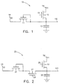
- Fig. 1 is a schematic diagram of a rudimentary embodiment of the invention.
- Fig. 2 shows a preferred embodiment of the invention.
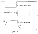
- Fig. 3 is a timing and waveform diagram for the circuit of Fig. 2.
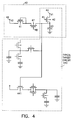
- Fig. 4 shows the invention serving, and merged with, a single target circuit.
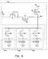
- Fig. 5 shows the invention serving, and merged with, multiple target circuits.
- FIG. 1 A rudimentary embodiment of the circuit of the invention is shown in Fig. 1.
- the circuit 10 comprises NMOS metering transistor 11, PMOS charging transistor 12, capacitor 13, first voltage supply V1 connected to terminal 14, second voltage supply V2 connected to terminal 16 and output terminal 100.
- Charging clock pulses are applied to terminal 15.
- Fig. 2 shows a more complete and preferred embodiment, having in addition to components corresponding to Fig. 1, PMOS blocking transistor 27 and blocking clock pulses applied to terminal 28. Operation will be described for Fig. 2 with the aid of the timing and waveform diagram of Fig. 3. The operation of Fig. 1 will be understood by simply deleting references to transistor 27 and its blocking clock pulses at 28.
- the function of the circuits of Figs. 1 and 2 is to act upon the voltage supplies V1 and V2 to produce at the output a reference voltage which is greater than V2 by the zero-current threshold voltage of metering transistor 11 (Fig. 1) or 21 (Fig. 2).
- Voltage supply V1 is at least incrementally greater than the largest output voltage to be obtained.
- the value of V2 is the difference between the desired minimum value of the output and the minimum of the range of the threshold voltage of Transistor 21.
- transistors 22 and 27 are off.
- Transistor 22 is turned on momentarily by charging clock pulse 35 (Fig. 3) at terminal 25, thus charging capacitor 23 toward V1 as shown as rising portion 391 of waveform 39 at terminal 200.
- Fig. 4 shows a preferred embodiment in which reference generator 40, in accordance with the invention, serves a single target circuit 440 and is merged with it such that charging transistor 42 and capacitor 43 are shared by reference generator 40 and target circuit 440.
- the target circuit metering transistor of which threshold variations are to be corrected is transistor 441. Operation of reference generator 40 is the same as described above and occurs at the time in the operating cycle of target circuit 440 when the output capacitor 43 of the first stage is to be charged to the reference voltage.
- metering transistor 41 should be located as close as possible to the metering transistor 441 of the target circuit, the threshold variation of which is to be corrected.
- Fig. 5 shows a preferred embodiment in which a reference generator 50, in accordance with the invention, serves several target circuits 550.
- the load capacitance of the reference generator (corresponding to 13, 23 and 43 of the previous embodiments) is provided by the parallel combination of capacitors 53' of all of the served target circuits, and is equal to the sum of their capacitances.
- the reference generator is merged with the target circuits. This case differs from that of Fig. 4 in that charging transistor 52 is not shared and a transistor 590 of each target circuit is interposed between reference generator output terminal 500 and the shared capacitors 53'.
- 590 is turned on approximately simultaneously with 52 and is turned off after the reference voltage has reached its final value across 53' but preferably before 52 turns off because that sequence minimizes possible charge injection errors.
- Metering transistor 51 of reference generator circuit 50 should be located as close as possible to a central position relative to the served target circuits to optimize threshold tracking.
Landscapes
- Semiconductor Integrated Circuits (AREA)
Applications Claiming Priority (2)
| Application Number | Priority Date | Filing Date | Title |
|---|---|---|---|
| US431933 | 1982-09-30 | ||
| US43193395A | 1995-05-01 | 1995-05-01 |
Publications (2)
| Publication Number | Publication Date |
|---|---|
| EP0741390A2 true EP0741390A2 (de) | 1996-11-06 |
| EP0741390A3 EP0741390A3 (de) | 1997-07-23 |
Family
ID=23714050
Family Applications (1)
| Application Number | Title | Priority Date | Filing Date |
|---|---|---|---|
| EP96103833A Withdrawn EP0741390A3 (de) | 1995-05-01 | 1996-03-12 | Referenzspannungsgenerator zum Korrigieren der Schwellspannung |
Country Status (2)
| Country | Link |
|---|---|
| US (1) | US5719523A (de) |
| EP (1) | EP0741390A3 (de) |
Families Citing this family (2)
| Publication number | Priority date | Publication date | Assignee | Title |
|---|---|---|---|---|
| JP2000242565A (ja) * | 1999-02-19 | 2000-09-08 | Nec Corp | 無線携帯端末 |
| US9136831B2 (en) * | 2011-07-05 | 2015-09-15 | India Institute Of Technology, Bombay | Frequency to voltage converter |
Family Cites Families (16)
| Publication number | Priority date | Publication date | Assignee | Title |
|---|---|---|---|---|
| US3621281A (en) * | 1969-09-12 | 1971-11-16 | Ferroxcube Corp | Linear rise and fall time current generator |
| JPS56122526A (en) * | 1980-03-03 | 1981-09-26 | Fujitsu Ltd | Semiconductor integrated circuit |
| JPS56129423A (en) * | 1980-03-14 | 1981-10-09 | Sony Corp | Triangle wave generating circuit |
| US4728828A (en) * | 1983-06-20 | 1988-03-01 | Santa Barbara Research Center | Switched capacitor transresistance amplifier |
| EP0190973B1 (de) * | 1985-02-04 | 1992-06-03 | Sony Corporation | Abtast- und Halteschaltung |
| JPS61269716A (ja) * | 1985-05-24 | 1986-11-29 | Hitachi Ltd | 電圧変換回路 |
| JP2501590B2 (ja) * | 1987-07-29 | 1996-05-29 | 沖電気工業株式会社 | 半導体装置の駆動回路 |
| JPH0673092B2 (ja) * | 1988-04-12 | 1994-09-14 | 日本電気株式会社 | 定電圧発生回路 |
| US5185721A (en) * | 1988-10-31 | 1993-02-09 | Texas Instruments Incorporated | Charge-retaining signal boosting circuit and method |
| JP2597739B2 (ja) * | 1990-08-24 | 1997-04-09 | 株式会社東芝 | 信号遅延回路、クロック信号発生回路及び集積回路システム |
| JPH04172711A (ja) * | 1990-11-06 | 1992-06-19 | Mitsubishi Electric Corp | 半導体遅延回路 |
| US5117177A (en) * | 1991-01-23 | 1992-05-26 | Ramtron Corporation | Reference generator for an integrated circuit |
| DE4130191C2 (de) * | 1991-09-30 | 1993-10-21 | Samsung Electronics Co Ltd | Konstantspannungsgenerator für eine Halbleitereinrichtung mit kaskadierter Auflade- bzw. Entladeschaltung |
| US5268871A (en) * | 1991-10-03 | 1993-12-07 | International Business Machines Corporation | Power supply tracking regulator for a memory array |
| US5303191A (en) * | 1992-01-23 | 1994-04-12 | Motorola, Inc. | Memory with compensation for voltage, temperature, and processing variations |
| US5400028A (en) * | 1992-10-30 | 1995-03-21 | International Business Machines Corporation | Charge summing digital to analog converter |
-
1996
- 1996-03-12 EP EP96103833A patent/EP0741390A3/de not_active Withdrawn
- 1996-11-12 US US08/747,985 patent/US5719523A/en not_active Expired - Fee Related
Also Published As
| Publication number | Publication date |
|---|---|
| US5719523A (en) | 1998-02-17 |
| EP0741390A3 (de) | 1997-07-23 |
Similar Documents
| Publication | Publication Date | Title |
|---|---|---|
| US6052426A (en) | Shift register using M.I.S. transistors of like polarity | |
| US7460634B2 (en) | Shift register circuit | |
| US6946905B2 (en) | Offset cancel circuit of voltage follower equipped with operational amplifier | |
| US6834095B2 (en) | Shift-register circuit | |
| US7005838B2 (en) | Voltage generation circuit | |
| JP2003248470A (ja) | レベル・シフタを内蔵したシフト・レジスタ | |
| JPH08263027A (ja) | シフトレジスタ | |
| US4255715A (en) | Offset correction circuit for differential amplifiers | |
| US5066870A (en) | Charge pump having pull-up circuit operating with two clock pulse sequences | |
| US4862016A (en) | High speed, low drift sample and hold circuit | |
| JP3289126B2 (ja) | ビデオ表示装置 | |
| US20050012542A1 (en) | Power supply | |
| US4952863A (en) | Voltage regulator with power boost system | |
| US4328434A (en) | Comparator circuit with offset correction | |
| US5719523A (en) | Threshold correcting reference voltage generator | |
| JPH0990917A (ja) | データ・ライン駆動回路 | |
| JPH08264758A (ja) | 電圧を高い線形性で複写する素子 | |
| JP2000194323A (ja) | アナログバッファ回路及び液晶表示装置 | |
| US5457415A (en) | Charge metering sampling circuit and use thereof in TFT/LCD | |
| JP2994000B2 (ja) | サンプル・ホールド増幅回路 | |
| US6956787B2 (en) | Method and device for timing random reading of a memory device | |
| JPH05134628A (ja) | 液晶表示体駆動装置 | |
| JP3979720B2 (ja) | サンプルアンドホールド回路 | |
| JP2803463B2 (ja) | トランスファゲート・トランジスタのゲート昇圧回路 | |
| US20240063766A1 (en) | Amplifier circuit |
Legal Events
| Date | Code | Title | Description |
|---|---|---|---|
| PUAI | Public reference made under article 153(3) epc to a published international application that has entered the european phase |
Free format text: ORIGINAL CODE: 0009012 |
|
| AK | Designated contracting states |
Kind code of ref document: A2 Designated state(s): DE FR GB |
|
| 17P | Request for examination filed |
Effective date: 19970325 |
|
| PUAL | Search report despatched |
Free format text: ORIGINAL CODE: 0009013 |
|
| AK | Designated contracting states |
Kind code of ref document: A3 Designated state(s): DE FR GB |
|
| STAA | Information on the status of an ep patent application or granted ep patent |
Free format text: STATUS: THE APPLICATION IS DEEMED TO BE WITHDRAWN |
|
| 18D | Application deemed to be withdrawn |
Effective date: 19980124 |