EP0741118A2 - Verfahren zur Ablation von synthetischen Diamanten mit Sauerstoffplasma und also geätzte synthetische Diamanten - Google Patents
Verfahren zur Ablation von synthetischen Diamanten mit Sauerstoffplasma und also geätzte synthetische Diamanten Download PDFInfo
- Publication number
- EP0741118A2 EP0741118A2 EP96201152A EP96201152A EP0741118A2 EP 0741118 A2 EP0741118 A2 EP 0741118A2 EP 96201152 A EP96201152 A EP 96201152A EP 96201152 A EP96201152 A EP 96201152A EP 0741118 A2 EP0741118 A2 EP 0741118A2
- Authority
- EP
- European Patent Office
- Prior art keywords
- diamond
- subjecting
- plasma etching
- approximately
- colloidal graphite
- Prior art date
- Legal status (The legal status is an assumption and is not a legal conclusion. Google has not performed a legal analysis and makes no representation as to the accuracy of the status listed.)
- Withdrawn
Links
Images

Classifications
-
- C—CHEMISTRY; METALLURGY
- C04—CEMENTS; CONCRETE; ARTIFICIAL STONE; CERAMICS; REFRACTORIES
- C04B—LIME, MAGNESIA; SLAG; CEMENTS; COMPOSITIONS THEREOF, e.g. MORTARS, CONCRETE OR LIKE BUILDING MATERIALS; ARTIFICIAL STONE; CERAMICS; REFRACTORIES; TREATMENT OF NATURAL STONE
- C04B41/00—After-treatment of mortars, concrete, artificial stone or ceramics; Treatment of natural stone
- C04B41/009—After-treatment of mortars, concrete, artificial stone or ceramics; Treatment of natural stone characterised by the material treated
-
- C—CHEMISTRY; METALLURGY
- C04—CEMENTS; CONCRETE; ARTIFICIAL STONE; CERAMICS; REFRACTORIES
- C04B—LIME, MAGNESIA; SLAG; CEMENTS; COMPOSITIONS THEREOF, e.g. MORTARS, CONCRETE OR LIKE BUILDING MATERIALS; ARTIFICIAL STONE; CERAMICS; REFRACTORIES; TREATMENT OF NATURAL STONE
- C04B41/00—After-treatment of mortars, concrete, artificial stone or ceramics; Treatment of natural stone
- C04B41/0054—Plasma-treatment, e.g. with gas-discharge plasma
-
- C—CHEMISTRY; METALLURGY
- C04—CEMENTS; CONCRETE; ARTIFICIAL STONE; CERAMICS; REFRACTORIES
- C04B—LIME, MAGNESIA; SLAG; CEMENTS; COMPOSITIONS THEREOF, e.g. MORTARS, CONCRETE OR LIKE BUILDING MATERIALS; ARTIFICIAL STONE; CERAMICS; REFRACTORIES; TREATMENT OF NATURAL STONE
- C04B41/00—After-treatment of mortars, concrete, artificial stone or ceramics; Treatment of natural stone
- C04B41/53—After-treatment of mortars, concrete, artificial stone or ceramics; Treatment of natural stone involving the removal of at least part of the materials of the treated article, e.g. etching, drying of hardened concrete
- C04B41/5338—Etching
- C04B41/5346—Dry etching
-
- C—CHEMISTRY; METALLURGY
- C04—CEMENTS; CONCRETE; ARTIFICIAL STONE; CERAMICS; REFRACTORIES
- C04B—LIME, MAGNESIA; SLAG; CEMENTS; COMPOSITIONS THEREOF, e.g. MORTARS, CONCRETE OR LIKE BUILDING MATERIALS; ARTIFICIAL STONE; CERAMICS; REFRACTORIES; TREATMENT OF NATURAL STONE
- C04B41/00—After-treatment of mortars, concrete, artificial stone or ceramics; Treatment of natural stone
- C04B41/80—After-treatment of mortars, concrete, artificial stone or ceramics; Treatment of natural stone of only ceramics
- C04B41/91—After-treatment of mortars, concrete, artificial stone or ceramics; Treatment of natural stone of only ceramics involving the removal of part of the materials of the treated articles, e.g. etching
-
- C—CHEMISTRY; METALLURGY
- C30—CRYSTAL GROWTH
- C30B—SINGLE-CRYSTAL GROWTH; UNIDIRECTIONAL SOLIDIFICATION OF EUTECTIC MATERIAL OR UNIDIRECTIONAL DEMIXING OF EUTECTOID MATERIAL; REFINING BY ZONE-MELTING OF MATERIAL; PRODUCTION OF A HOMOGENEOUS POLYCRYSTALLINE MATERIAL WITH DEFINED STRUCTURE; SINGLE CRYSTALS OR HOMOGENEOUS POLYCRYSTALLINE MATERIAL WITH DEFINED STRUCTURE; AFTER-TREATMENT OF SINGLE CRYSTALS OR A HOMOGENEOUS POLYCRYSTALLINE MATERIAL WITH DEFINED STRUCTURE; APPARATUS THEREFOR
- C30B29/00—Single crystals or homogeneous polycrystalline material with defined structure characterised by the material or by their shape
- C30B29/02—Elements
- C30B29/04—Diamond
-
- C—CHEMISTRY; METALLURGY
- C30—CRYSTAL GROWTH
- C30B—SINGLE-CRYSTAL GROWTH; UNIDIRECTIONAL SOLIDIFICATION OF EUTECTIC MATERIAL OR UNIDIRECTIONAL DEMIXING OF EUTECTOID MATERIAL; REFINING BY ZONE-MELTING OF MATERIAL; PRODUCTION OF A HOMOGENEOUS POLYCRYSTALLINE MATERIAL WITH DEFINED STRUCTURE; SINGLE CRYSTALS OR HOMOGENEOUS POLYCRYSTALLINE MATERIAL WITH DEFINED STRUCTURE; AFTER-TREATMENT OF SINGLE CRYSTALS OR A HOMOGENEOUS POLYCRYSTALLINE MATERIAL WITH DEFINED STRUCTURE; APPARATUS THEREFOR
- C30B33/00—After-treatment of single crystals or homogeneous polycrystalline material with defined structure
-
- H—ELECTRICITY
- H10—SEMICONDUCTOR DEVICES; ELECTRIC SOLID-STATE DEVICES NOT OTHERWISE PROVIDED FOR
- H10P—GENERIC PROCESSES OR APPARATUS FOR THE MANUFACTURE OR TREATMENT OF DEVICES COVERED BY CLASS H10
- H10P50/00—Etching of wafers, substrates or parts of devices
- H10P50/20—Dry etching; Plasma etching; Reactive-ion etching
- H10P50/24—Dry etching; Plasma etching; Reactive-ion etching of semiconductor materials
- H10P50/242—Dry etching; Plasma etching; Reactive-ion etching of semiconductor materials of Group IV materials
-
- C—CHEMISTRY; METALLURGY
- C04—CEMENTS; CONCRETE; ARTIFICIAL STONE; CERAMICS; REFRACTORIES
- C04B—LIME, MAGNESIA; SLAG; CEMENTS; COMPOSITIONS THEREOF, e.g. MORTARS, CONCRETE OR LIKE BUILDING MATERIALS; ARTIFICIAL STONE; CERAMICS; REFRACTORIES; TREATMENT OF NATURAL STONE
- C04B2111/00—Mortars, concrete or artificial stone or mixtures to prepare them, characterised by specific function, property or use
- C04B2111/00474—Uses not provided for elsewhere in C04B2111/00
- C04B2111/00844—Uses not provided for elsewhere in C04B2111/00 for electronic applications
Definitions
- the invention relates to the etching of synthetic diamond in an oxygen plasma. More particularly, the invention relates to methods of coating a synthetic diamond prior to plasma etching such that the density and depth of surface pits in the diamond are reduced subsequent to plasma etching and to finished diamonds prepared in this manner.
- a diamond is an allotrope of carbon exhibiting a crystallographic network of exclusively covalently bonded, aliphatic sp 3 hybridized carbon atoms arranged tetrahedrally with a uniform distance of 1.545 ⁇ between atoms. Due to this structure, diamonds are extremely hard and have a thermal conductivity approximately four times that of copper while being an electrical insulator. Although diamonds are most popularly known for their gemstone qualities, their hardness, thermal and electrical properties make them very useful for many industrial applications.
- CVD chemical vapor deposition
- One of the persistent undesired features of diamond wafers manufactured by CVD is that of large surface irregularities (pits).
- pits For most applications, it is necessary to smooth or polish (ablate) the surface of the diamond film to obtain the proper thickness tolerance and/or surface finish.
- specialized tools are required for accurately machining the surface of the diamond film to the desired finish.
- Typical methods for mechanical diamond finishing involve abrading the diamond film with a diamond grit slurry on a lapping machine. These methods tend to be costly and time consuming, often entailing ablating rates of about 0.1 mm/hr to 0.1 mm/min and requiring up to several months to finish a four inch diameter diamond wafer.
- laser ablation is accomplished by irradiating the surface of the diamond with a laser beam at an angle, such that the convex irregularities on the surface are exposed to a higher laser power density than the planar areas, and the concave irregularities are shielded by the convex ones.
- the surface of the diamond undergoes several passes under the laser to evenly smooth the surface and the laser typically removes from 10 to 40 microns of diamond per pass under the laser.
- a current technique for etching a diamond wafer is known as oxygen plasma etching with pattern masking.
- oxygen plasma etching a diamond wafer is lithographically patterned with photoresist or with sputtered Ti-Pt-Au.
- the masked wafer is placed in a reactor with oxygen under pressure of 1 to 30 mtorr.
- Microwave powers of 200 to 700 watts and DC biases of -50 to -300 volts are induced in the reactor by applying 13.56 MHz (an FCC allocated frequency) RF power to a cathode.
- Plasma etching can achieve an etch rate of 5 to 10 microns/hr which is substantially faster than other methods.
- the influence of various parameters on the etch rate of the diamond wafer is discussed by Pearton et al. in "ECR Plasma Etching of Chemically Vapor Deposited Diamond Thin Films", Electronics Letters , 23 April 1992, Vol. 28., No. 9, pp. 822-824.
- the authors conclude that Ti-Pt-Au is more resistant to etching than photoresist and has other advantages in that it performs a self-aligned contact to the diamond.
- the plasma etching is highly anisotropic at low pressure and the surface morphology of the diamond is substantially the same after etching as it was prior to etching. That is, pits are not removed.
- the method of the present invention includes applying colloidal graphite to the surface of a diamond wafer and then subjecting the wafer to an oxygen plasma.
- the oxygen plasma is permitted to remove approximately 50 microns of diamond so that the pits are removed (or more accurately, the diamond between the pits is removed down to the bottom of the pits).
- the wafer is then preferably mechanically lapped. The resulting surface of the wafer is virtually pit free.
- FIG. 1 the method of the invention is seen.
- a CVD diamond sample is obtained.
- Colloidal graphite graphite particles preferably having a mean diameter of approximately 1 micron suspended in a solvent
- the surface bearing the colloidal graphite is subjected to oxygen plasma etching at 14.
- the surface bearing the colloidal graphite is cleaned at 13.
- the surface upon which the colloidal graphite was applied is optionally lapped at 15.
- a diamond wafer formed by a CVD process, and having a diameter of approximately 100mm was subjected to plasma etching on the substrate side for approximately nine hours.
- the average removal of diamond from the wafer was approximately 41.0 microns with a standard deviation of approximately 6.5 microns.
- Commercial grade colloidal graphite (graphite suspended in a solution of water and alcohol) was then applied to a 15mm wide strip of both sides of the wafer.
- the wafer was then subjected to a second etching procedure on its deposition side where the average removal of diamond from the wafer was approximately 45.6 microns with a standard deviation of approximately 16.0 microns.
- the wafer was then subjected to a third etching to remove approximately 50 microns from the deposition side.
- etchings were performed in a reactor in the presence of oxygen, argon, and SF 6 under a pressure of 4 mtorr.
- Input power to the reactor was held constant at 600 W and the RF bias was held to a constant maximum -118 V.
- the flow rates of oxygen, argon and SF 6 were fixed at 28, 6, and 2 sccm, respectively.
- the input power to the reactor may be varied from about 500 to 1500 W and the RF bias may be varied from about -100 to -300 V. While oxygen is generally considered to be necessary to the etching process, argon and SF 6 may not be necessary to achieve the desired results. Argon is used to help ignite the ECR plasma, but the process will probably work without argon.
- SF 6 prevents the formation of black film which may be acceptable in some applications.
- the flow rates of oxygen, argon and SF 6 may be varied from 20-40, 0-20, and 1-4 sccm, respectively.
- the pressure of the reactor may be varied from 2-10 mtorr.
- the wafer was mounted in a lapping machine.
- the deposition side of the diamond wafer was mechanically lapped for approximately sixty-three hours.
- Visual inspection of the wafer after lapping revealed an absence of pits on the portion of the wafer which had been coated with colloidal graphite.
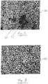
- the wafer was lapped an additional twenty-one hours and micrographs were taken of the lapped surface.
- Figure 2 is a micrograph (65x magnification) of a portion 20 of the deposition side of the diamond wafer which was not coated with colloidal graphite.
- the large dark spots 25, 30 in Figure 2 represent pits in the surface of the diamond. These pits are on the order of 50 microns deep.
- Figure 3 is a micrograph (65x magnification) of a portion 40 of the deposition side of the diamond wafer which was coated with colloidal graphite. The absence of large dark spots in Figure 3 represents a pit-free surface of the diamond wafer.
Landscapes
- Chemical & Material Sciences (AREA)
- Engineering & Computer Science (AREA)
- Ceramic Engineering (AREA)
- Materials Engineering (AREA)
- Organic Chemistry (AREA)
- Structural Engineering (AREA)
- Metallurgy (AREA)
- Crystallography & Structural Chemistry (AREA)
- Plasma & Fusion (AREA)
- Physics & Mathematics (AREA)
- Crystals, And After-Treatments Of Crystals (AREA)
- Physical Or Chemical Processes And Apparatus (AREA)
- Carbon And Carbon Compounds (AREA)
Applications Claiming Priority (2)
| Application Number | Priority Date | Filing Date | Title |
|---|---|---|---|
| US437102 | 1995-05-05 | ||
| US08/437,102 US5711698A (en) | 1995-05-05 | 1995-05-05 | Method of synthetic diamond ablation with an oxygen plasma and synthetic diamonds etched accordingly |
Publications (2)
| Publication Number | Publication Date |
|---|---|
| EP0741118A2 true EP0741118A2 (de) | 1996-11-06 |
| EP0741118A3 EP0741118A3 (de) | 1997-05-07 |
Family
ID=23735076
Family Applications (1)
| Application Number | Title | Priority Date | Filing Date |
|---|---|---|---|
| EP96201152A Withdrawn EP0741118A3 (de) | 1995-05-05 | 1996-04-26 | Verfahren zur Ablation von synthetischen Diamanten mit Sauerstoffplasma und also geätzte synthetische Diamanten |
Country Status (4)
| Country | Link |
|---|---|
| US (1) | US5711698A (de) |
| EP (1) | EP0741118A3 (de) |
| JP (1) | JPH08301692A (de) |
| CA (1) | CA2175787C (de) |
Cited By (1)
| Publication number | Priority date | Publication date | Assignee | Title |
|---|---|---|---|---|
| US8193538B2 (en) | 2007-01-22 | 2012-06-05 | Diamond Microwave Devices Limited | Electronic field effect devices |
Families Citing this family (8)
| Publication number | Priority date | Publication date | Assignee | Title |
|---|---|---|---|---|
| JP3971090B2 (ja) * | 2000-04-05 | 2007-09-05 | 株式会社神戸製鋼所 | 針状表面を有するダイヤモンドの製造方法及び繊毛状表面を有する炭素系材料の製造方法 |
| US20020170897A1 (en) * | 2001-05-21 | 2002-11-21 | Hall Frank L. | Methods for preparing ball grid array substrates via use of a laser |
| CN100390331C (zh) * | 2005-09-22 | 2008-05-28 | 武汉化工学院 | 一种抛光大面积金刚石膜的方法和装置 |
| US8227350B2 (en) * | 2008-01-04 | 2012-07-24 | Advanced Diamond Technologies, Inc. | Controlling diamond film surfaces and layering |
| US20090214826A1 (en) * | 2008-01-04 | 2009-08-27 | Charles West | Controlling diamond film surfaces |
| US8342164B2 (en) * | 2008-05-09 | 2013-01-01 | SCIO Diamond Technology Corporation | Gemstone production from CVD diamond plate |
| JP6699015B2 (ja) * | 2016-02-29 | 2020-05-27 | 信越化学工業株式会社 | ダイヤモンド基板の製造方法 |
| CN118456269A (zh) * | 2024-06-14 | 2024-08-09 | 哈尔滨工业大学 | 基于激光与超精密磨削的cvd金刚石加工方法 |
Family Cites Families (5)
| Publication number | Priority date | Publication date | Assignee | Title |
|---|---|---|---|---|
| JPS6462484A (en) * | 1987-09-02 | 1989-03-08 | Seiko Instr & Electronics | Method for flattening diamond film |
| JPH0393694A (ja) * | 1989-09-06 | 1991-04-18 | Sumitomo Electric Ind Ltd | 砥粒の製造方法 |
| US5500077A (en) * | 1993-03-10 | 1996-03-19 | Sumitomo Electric Industries, Ltd. | Method of polishing/flattening diamond |
| GB2281254B (en) * | 1993-08-23 | 1996-11-27 | Northern Telecom Ltd | Polishing polycrystalline films |
| US5472370A (en) * | 1994-07-29 | 1995-12-05 | University Of Arkansas | Method of planarizing polycrystalline diamonds, planarized polycrystalline diamonds and products made therefrom |
-
1995
- 1995-05-05 US US08/437,102 patent/US5711698A/en not_active Expired - Fee Related
-
1996
- 1996-04-26 EP EP96201152A patent/EP0741118A3/de not_active Withdrawn
- 1996-05-03 CA CA002175787A patent/CA2175787C/en not_active Expired - Fee Related
- 1996-05-07 JP JP8137645A patent/JPH08301692A/ja active Pending
Cited By (6)
| Publication number | Priority date | Publication date | Assignee | Title |
|---|---|---|---|---|
| US8193538B2 (en) | 2007-01-22 | 2012-06-05 | Diamond Microwave Devices Limited | Electronic field effect devices |
| US8277622B2 (en) | 2007-01-22 | 2012-10-02 | Element Six Ltd. | High uniformity boron doped diamond material |
| US8362492B2 (en) | 2007-01-22 | 2013-01-29 | Diamond Microwave Devices Limited | Electronic field effect devices and methods for their manufacture |
| US8648354B2 (en) | 2007-01-22 | 2014-02-11 | Diamond Microwave Devices Limited | Electronic field effect devices and methods for their manufacture |
| US9034200B2 (en) | 2007-01-22 | 2015-05-19 | Element Six Limited Technologies Limited | Plasma etching of diamond surfaces |
| US10011491B2 (en) | 2007-01-22 | 2018-07-03 | Element Six Technologies Limited | Plasma etching of diamond surfaces |
Also Published As
| Publication number | Publication date |
|---|---|
| US5711698A (en) | 1998-01-27 |
| CA2175787C (en) | 1999-08-10 |
| EP0741118A3 (de) | 1997-05-07 |
| CA2175787A1 (en) | 1996-11-06 |
| JPH08301692A (ja) | 1996-11-19 |
Similar Documents
| Publication | Publication Date | Title |
|---|---|---|
| US5458733A (en) | Method for etching a diamond film | |
| US7226869B2 (en) | Methods for protecting silicon or silicon carbide electrode surfaces from morphological modification during plasma etch processing | |
| EP2108054B1 (de) | Plasmaätzen von diamantoberflächen | |
| US5990013A (en) | Process for treating a semiconductor substrate comprising a surface-treatment step | |
| Leech et al. | Reactive ion etching of diamond in CF4, O2, O2 and Ar-based mixtures | |
| EP0676772B1 (de) | Herstellungsverfahren für Röntgenstrahlenfenster | |
| EP0637067A2 (de) | Plasma-Ätzen mit Xenon | |
| JPH05500883A (ja) | 結晶成長用の炭化珪素表面を加工する方法 | |
| KR101332206B1 (ko) | 반도체 처리 방법 | |
| TW200524833A (en) | Methods of finishing quartz glass surfaces and components made by the methods | |
| Buchkremer-Hermanns et al. | ECR plasma polishing of CVD diamond films | |
| US5711698A (en) | Method of synthetic diamond ablation with an oxygen plasma and synthetic diamonds etched accordingly | |
| US5639551A (en) | Low pressure growth of cubic boron nitride films | |
| EP0419087B1 (de) | Verfahren zur Herstellung von Schleifmitteln | |
| US7208325B2 (en) | Refreshing wafers having low-k dielectric materials | |
| EP0931177B1 (de) | Nachbehandelter diamantbeschichteter körper | |
| US6168744B1 (en) | Process for sequential multi beam laser processing of materials | |
| EP0146446B1 (de) | Verfahren und Vorrichtung zur Plasmabehandlung von Halbleitermaterialien | |
| Sirineni et al. | Reactive ion etching of diamond as a means of enhancing chemically-assisted mechanical polishing efficiency | |
| US20230367339A1 (en) | Methods for preparing void-free coatings for plasma treatment components | |
| Cerva et al. | Transmission electron microscope study of lattice damage and polymer coating formed after reactive ion etching of SiO2 | |
| JP2001217226A (ja) | 半導体装置の製造装置及びその製造方法 | |
| JP3453337B2 (ja) | 炭素または炭素を主成分とする被膜を形成する反応室のクリーニング方法 | |
| JP3513811B2 (ja) | 炭素または炭素を主成分とする被膜の形成方法 | |
| GB2288272A (en) | X-ray windows |
Legal Events
| Date | Code | Title | Description |
|---|---|---|---|
| PUAI | Public reference made under article 153(3) epc to a published international application that has entered the european phase |
Free format text: ORIGINAL CODE: 0009012 |
|
| AK | Designated contracting states |
Kind code of ref document: A2 Designated state(s): DE FR GB |
|
| PUAL | Search report despatched |
Free format text: ORIGINAL CODE: 0009013 |
|
| AK | Designated contracting states |
Kind code of ref document: A3 Designated state(s): DE FR GB |
|
| 17P | Request for examination filed |
Effective date: 19971023 |
|
| RAP1 | Party data changed (applicant data changed or rights of an application transferred) |
Owner name: SAINT-GOBAIN INDUSTRIAL CERAMICS, INC. |
|
| 17Q | First examination report despatched |
Effective date: 19981106 |
|
| STAA | Information on the status of an ep patent application or granted ep patent |
Free format text: STATUS: THE APPLICATION IS DEEMED TO BE WITHDRAWN |
|
| 18D | Application deemed to be withdrawn |
Effective date: 20020712 |