EP0735604A1 - Dielektrische Planarleitung und integrierte Schaltung die dieselbe benutzt - Google Patents
Dielektrische Planarleitung und integrierte Schaltung die dieselbe benutzt Download PDFInfo
- Publication number
- EP0735604A1 EP0735604A1 EP96104889A EP96104889A EP0735604A1 EP 0735604 A1 EP0735604 A1 EP 0735604A1 EP 96104889 A EP96104889 A EP 96104889A EP 96104889 A EP96104889 A EP 96104889A EP 0735604 A1 EP0735604 A1 EP 0735604A1
- Authority
- EP
- European Patent Office
- Prior art keywords
- dielectric
- substrate
- slot
- dielectric substrate
- frequency
- Prior art date
- Legal status (The legal status is an assumption and is not a legal conclusion. Google has not performed a legal analysis and makes no representation as to the accuracy of the status listed.)
- Granted
Links
- 239000000758 substrate Substances 0.000 claims abstract description 229
- 230000005540 biological transmission Effects 0.000 claims description 17
- 230000001902 propagating effect Effects 0.000 claims description 13
- 239000004020 conductor Substances 0.000 abstract description 8
- 239000003989 dielectric material Substances 0.000 abstract 1
- 230000005684 electric field Effects 0.000 description 16
- 230000005672 electromagnetic field Effects 0.000 description 15
- 238000010586 diagram Methods 0.000 description 12
- 238000010276 construction Methods 0.000 description 5
- NCGICGYLBXGBGN-UHFFFAOYSA-N 3-morpholin-4-yl-1-oxa-3-azonia-2-azanidacyclopent-3-en-5-imine;hydrochloride Chemical compound Cl.[N-]1OC(=N)C=[N+]1N1CCOCC1 NCGICGYLBXGBGN-UHFFFAOYSA-N 0.000 description 4
- 230000002238 attenuated effect Effects 0.000 description 4
- 230000004048 modification Effects 0.000 description 4
- 238000012986 modification Methods 0.000 description 4
- 230000000644 propagated effect Effects 0.000 description 3
- 230000015572 biosynthetic process Effects 0.000 description 2
- 230000004069 differentiation Effects 0.000 description 2
- 238000000034 method Methods 0.000 description 2
- 239000000783 alginic acid Substances 0.000 description 1
- 239000004106 carminic acid Substances 0.000 description 1
- 230000008859 change Effects 0.000 description 1
- 238000004891 communication Methods 0.000 description 1
- 230000000052 comparative effect Effects 0.000 description 1
- 230000008878 coupling Effects 0.000 description 1
- 238000010168 coupling process Methods 0.000 description 1
- 238000005859 coupling reaction Methods 0.000 description 1
- 238000011161 development Methods 0.000 description 1
- 230000002452 interceptive effect Effects 0.000 description 1
- 238000004519 manufacturing process Methods 0.000 description 1
- 238000010295 mobile communication Methods 0.000 description 1
- 239000012466 permeate Substances 0.000 description 1
- 238000009877 rendering Methods 0.000 description 1
- 238000011160 research Methods 0.000 description 1
- 239000013585 weight reducing agent Substances 0.000 description 1
Images
Classifications
-
- H—ELECTRICITY
- H01—ELECTRIC ELEMENTS
- H01P—WAVEGUIDES; RESONATORS, LINES, OR OTHER DEVICES OF THE WAVEGUIDE TYPE
- H01P3/00—Waveguides; Transmission lines of the waveguide type
- H01P3/02—Waveguides; Transmission lines of the waveguide type with two longitudinal conductors
-
- H—ELECTRICITY
- H01—ELECTRIC ELEMENTS
- H01P—WAVEGUIDES; RESONATORS, LINES, OR OTHER DEVICES OF THE WAVEGUIDE TYPE
- H01P3/00—Waveguides; Transmission lines of the waveguide type
-
- H—ELECTRICITY
- H01—ELECTRIC ELEMENTS
- H01L—SEMICONDUCTOR DEVICES NOT COVERED BY CLASS H10
- H01L2924/00—Indexing scheme for arrangements or methods for connecting or disconnecting semiconductor or solid-state bodies as covered by H01L24/00
- H01L2924/0001—Technical content checked by a classifier
- H01L2924/0002—Not covered by any one of groups H01L24/00, H01L24/00 and H01L2224/00
-
- H—ELECTRICITY
- H05—ELECTRIC TECHNIQUES NOT OTHERWISE PROVIDED FOR
- H05K—PRINTED CIRCUITS; CASINGS OR CONSTRUCTIONAL DETAILS OF ELECTRIC APPARATUS; MANUFACTURE OF ASSEMBLAGES OF ELECTRICAL COMPONENTS
- H05K1/00—Printed circuits
- H05K1/02—Details
- H05K1/0213—Electrical arrangements not otherwise provided for
- H05K1/0237—High frequency adaptations
Definitions
- transmission lines have been largely used in the range of microwave and millimeter-waves, such as waveguides, coaxial lines, microstrip lines, coplanar lines, slotted lines, and so on. These transmission lines are constructed by forming predetermined electrodes on a dielectric substrate. Waveguides are for use in applications where conductor losses should be inhibited to a low level.
- Coaxial lines are widely used as connecting cables between equipment.
- Coplanar lines, microstrip lines, slotted lines, etc. are largely employed for forming connections between electronic parts, such as ICs, since they are easily connected thereto.
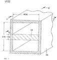
- the dielectric constant ⁇ r 23 and the thickness t23 of the dielectric substrate 23 and the dielectric constant ⁇ r 26 and ⁇ r 27 of the substrates 26 and 27, respectively, are set so that a planar wave having a propagation frequency fb is totally reflected on the top surface of the dielectric substrate 23 in the slot 24 and on the bottom surface of the substrate 23 close to the slot 25.
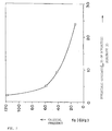
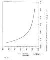
- Fig. 10 is a diagram indicating the relation between the frequency and the phase constant ⁇ 20 of the dielectric line LN20 when the widths W of the slots 24 and 25 of the substrate 23 were set at the values 0.5 mm, 1 mm, 2 mm and 3 mm.
- the values shown in Fig. 10 were calculated according to the finite-element method.
- the parameters of the structure of the dielectric line LN20 were set as follows:
Landscapes
- Waveguides (AREA)
- Semiconductor Integrated Circuits (AREA)
- Control Of Motors That Do Not Use Commutators (AREA)
Applications Claiming Priority (3)
| Application Number | Priority Date | Filing Date | Title |
|---|---|---|---|
| JP7069867A JP2991076B2 (ja) | 1995-03-28 | 1995-03-28 | 平面誘電体線路及び集積回路 |
| JP69867/95 | 1995-03-28 | ||
| JP6986795 | 1995-03-28 |
Publications (2)
| Publication Number | Publication Date |
|---|---|
| EP0735604A1 true EP0735604A1 (de) | 1996-10-02 |
| EP0735604B1 EP0735604B1 (de) | 2003-02-26 |
Family
ID=13415181
Family Applications (1)
| Application Number | Title | Priority Date | Filing Date |
|---|---|---|---|
| EP96104889A Expired - Lifetime EP0735604B1 (de) | 1995-03-28 | 1996-03-27 | Dielektrische Planarleitung und integrierte Schaltung die dieselbe benutzt |
Country Status (6)
| Country | Link |
|---|---|
| EP (1) | EP0735604B1 (de) |
| JP (1) | JP2991076B2 (de) |
| KR (1) | KR0177909B1 (de) |
| CN (2) | CN1226805C (de) |
| CA (1) | CA2172888C (de) |
| DE (1) | DE69626332T2 (de) |
Cited By (5)
| Publication number | Priority date | Publication date | Assignee | Title |
|---|---|---|---|---|
| EP0871239A1 (de) * | 1997-04-10 | 1998-10-14 | Murata Manufacturing Co., Ltd. | Antennen-Vorrichtung und Radarmodul |
| EP0862215A3 (de) * | 1997-02-27 | 1999-09-29 | Murata Manufacturing Co., Ltd. | Dielektrische integrierte Planarschaltung |
| EP0862216A3 (de) * | 1997-02-27 | 1999-10-06 | Murata Manufacturing Co., Ltd. | Dielektrische integrierte Planarschaltung |
| EP0883204A3 (de) * | 1997-06-05 | 1999-11-17 | Murata Manufacturing Co., Ltd. | Nichtstrahlende planare dielektrische Leitung und integrierte Schaltung damit |
| US6166614A (en) * | 1997-04-03 | 2000-12-26 | Murata Manufacturing Co., Ltd. | Nonradiative planar dielectric line and integrated circuit |
Families Citing this family (9)
| Publication number | Priority date | Publication date | Assignee | Title |
|---|---|---|---|---|
| JP3678194B2 (ja) | 2001-12-04 | 2005-08-03 | 株式会社村田製作所 | 伝送線路および送受信装置 |
| JP3695395B2 (ja) | 2002-01-09 | 2005-09-14 | 株式会社村田製作所 | 伝送線路および送受信装置 |
| US7365618B2 (en) | 2005-12-06 | 2008-04-29 | Murata Manufacturing Co., Ltd. | High-frequency circuit device, high-frequency module, and communication apparatus |
| US9478840B2 (en) * | 2012-08-24 | 2016-10-25 | City University Of Hong Kong | Transmission line and methods for fabricating thereof |
| JP6279977B2 (ja) * | 2014-06-02 | 2018-02-14 | モレックス エルエルシー | 導波体 |
| CN112738985B (zh) * | 2021-02-04 | 2022-04-08 | 华勤技术股份有限公司 | 电路板组件及电子设备 |
| CN115144962B (zh) * | 2021-03-31 | 2024-02-06 | 南京星隐科技发展有限公司 | 电磁波传输结构、器件及光芯片 |
| WO2022205124A1 (zh) * | 2021-03-31 | 2022-10-06 | 南京星隐科技发展有限公司 | 电磁波传输结构、器件及光芯片 |
| CN114552155B (zh) * | 2022-04-25 | 2022-07-05 | 电子科技大学成都学院 | 双模传输线 |
Citations (3)
| Publication number | Priority date | Publication date | Assignee | Title |
|---|---|---|---|---|
| US3026490A (en) * | 1959-12-28 | 1962-03-20 | Bell Telephone Labor Inc | Microwave coupling arrangements |
| EP0040067A1 (de) * | 1980-05-12 | 1981-11-18 | Junkosha Co. Ltd. | Streifenleiterkabel |
| EP0244105A2 (de) * | 1986-04-16 | 1987-11-04 | Hewlett-Packard Company | Integrierte Kapazitätsstrukturen in Mikrowellenflossenleitungsvorrichtungen |
Family Cites Families (1)
| Publication number | Priority date | Publication date | Assignee | Title |
|---|---|---|---|---|
| JP5345509B2 (ja) | 2009-11-22 | 2013-11-20 | 日本ポリプロ株式会社 | 加熱殺菌処理食品の包装フィルム用ポリプロピレン系樹脂組成物、及びそれを用いて得られる加熱殺菌処理食品の包装用フィルム |
-
1995
- 1995-03-28 JP JP7069867A patent/JP2991076B2/ja not_active Expired - Lifetime
-
1996
- 1996-03-27 DE DE69626332T patent/DE69626332T2/de not_active Expired - Lifetime
- 1996-03-27 EP EP96104889A patent/EP0735604B1/de not_active Expired - Lifetime
- 1996-03-28 KR KR1019960008848A patent/KR0177909B1/ko not_active Expired - Lifetime
- 1996-03-28 CN CNB031462995A patent/CN1226805C/zh not_active Expired - Lifetime
- 1996-03-28 CN CN96107349A patent/CN1120542C/zh not_active Expired - Lifetime
- 1996-03-28 CA CA002172888A patent/CA2172888C/en not_active Expired - Lifetime
Patent Citations (3)
| Publication number | Priority date | Publication date | Assignee | Title |
|---|---|---|---|---|
| US3026490A (en) * | 1959-12-28 | 1962-03-20 | Bell Telephone Labor Inc | Microwave coupling arrangements |
| EP0040067A1 (de) * | 1980-05-12 | 1981-11-18 | Junkosha Co. Ltd. | Streifenleiterkabel |
| EP0244105A2 (de) * | 1986-04-16 | 1987-11-04 | Hewlett-Packard Company | Integrierte Kapazitätsstrukturen in Mikrowellenflossenleitungsvorrichtungen |
Non-Patent Citations (2)
| Title |
|---|
| H.C.C. FERNANDES ET AL.: "Metallization thickness in bilateral and unilateral finlines", INTERNATIONAL JOURNAL OF INFRARED AND MILLIMETER WAVES, vol. 15, no. 6, June 1994 (1994-06-01), NEW YORK US, pages 1001 - 1014, XP000454389 * |
| J.J. LEE: "Slotline impedance", IEEE TRANSACTIONS ON MICROWAVE THEORY AND TECHNIQUES, vol. 39, no. 4, April 1991 (1991-04-01), NEW YORK US, pages 666 - 672, XP000179063 * |
Cited By (9)
| Publication number | Priority date | Publication date | Assignee | Title |
|---|---|---|---|---|
| EP0862215A3 (de) * | 1997-02-27 | 1999-09-29 | Murata Manufacturing Co., Ltd. | Dielektrische integrierte Planarschaltung |
| EP0862216A3 (de) * | 1997-02-27 | 1999-10-06 | Murata Manufacturing Co., Ltd. | Dielektrische integrierte Planarschaltung |
| US6169301B1 (en) | 1997-02-27 | 2001-01-02 | Murata Manufacturing Co., Ltd. | Planar dielectric integrated circuit |
| US6445255B1 (en) | 1997-02-27 | 2002-09-03 | Murata Manufacturing Co., Ltd. | Planar dielectric integrated circuit |
| US6717492B2 (en) * | 1997-02-27 | 2004-04-06 | Murata Manufacturing Co., Ltd. | Planar dielectric integrated circuit with line conversion conductor patterns |
| US6166614A (en) * | 1997-04-03 | 2000-12-26 | Murata Manufacturing Co., Ltd. | Nonradiative planar dielectric line and integrated circuit |
| EP0871239A1 (de) * | 1997-04-10 | 1998-10-14 | Murata Manufacturing Co., Ltd. | Antennen-Vorrichtung und Radarmodul |
| US6052087A (en) * | 1997-04-10 | 2000-04-18 | Murata Manufacturing Co., Ltd. | Antenna device and radar module |
| EP0883204A3 (de) * | 1997-06-05 | 1999-11-17 | Murata Manufacturing Co., Ltd. | Nichtstrahlende planare dielektrische Leitung und integrierte Schaltung damit |
Also Published As
| Publication number | Publication date |
|---|---|
| JP2991076B2 (ja) | 1999-12-20 |
| KR960036193A (ko) | 1996-10-28 |
| DE69626332D1 (de) | 2003-04-03 |
| CN1144406A (zh) | 1997-03-05 |
| EP0735604B1 (de) | 2003-02-26 |
| DE69626332T2 (de) | 2003-11-27 |
| KR0177909B1 (ko) | 1999-05-15 |
| CA2172888A1 (en) | 1996-09-29 |
| JPH08265007A (ja) | 1996-10-11 |
| CN1479406A (zh) | 2004-03-03 |
| CN1120542C (zh) | 2003-09-03 |
| CN1226805C (zh) | 2005-11-09 |
| CA2172888C (en) | 2005-05-24 |
Similar Documents
| Publication | Publication Date | Title |
|---|---|---|
| US5986527A (en) | Planar dielectric line and integrated circuit using the same line | |
| KR100292763B1 (ko) | 안테나장치및레이더모듈 | |
| Uchimura et al. | Development of a" laminated waveguide" | |
| EP1049192B1 (de) | Hochfrequenz-Kommunikationsgerät | |
| US6870438B1 (en) | Multi-layered wiring board for slot coupling a transmission line to a waveguide | |
| US7154441B2 (en) | Device for transmitting or emitting high-frequency waves | |
| EP0735604B1 (de) | Dielektrische Planarleitung und integrierte Schaltung die dieselbe benutzt | |
| JP2004153367A (ja) | 高周波モジュール、ならびにモード変換構造および方法 | |
| CN110098485A (zh) | 小间距微带天线阵列 | |
| EP0898322B1 (de) | Dielektrischer Wellenleiter und dessen Abzweigstruktur | |
| KR101812490B1 (ko) | 기판 집적형 도파관의 표면실장을 위한 전이구조 설계 및 그 제조방법 | |
| JP2005051331A (ja) | マイクロストリップ線路と誘電体導波管との結合構造 | |
| US20220407204A1 (en) | Microwave system and apparatus | |
| Yamazaki et al. | Broadband differential-line-to-waveguide transition in multi-layer dielectric substrates with an X-shaped patch element in 280 GHz band | |
| JPH11340701A (ja) | 高周波伝送線路の接続構造 | |
| JP3013798B2 (ja) | 交差線路 | |
| US6727776B2 (en) | Device for propagating radio frequency signals in planar circuits | |
| US6535089B1 (en) | High-frequency circuit device and communication apparatus using the same | |
| EP0883204B1 (de) | Nichtstrahlende planare dielektrische Leitung und integrierte Schaltung damit | |
| CN116868697A (zh) | 印刷布线板 | |
| US6166614A (en) | Nonradiative planar dielectric line and integrated circuit | |
| JP2000077912A (ja) | 誘電体導波管線路の接続構造 | |
| JP7113986B2 (ja) | 変換器、及びアンテナ装置 | |
| WO2011136737A1 (en) | Silicon based millimeter wave waveguide transition | |
| Chokchai et al. | Broadband GCPW-to-Waveguide Transition in Multi-Layer Dielectric Substrate with Double Patch and Corrugation Structures in 275 GHz Band |
Legal Events
| Date | Code | Title | Description |
|---|---|---|---|
| PUAI | Public reference made under article 153(3) epc to a published international application that has entered the european phase |
Free format text: ORIGINAL CODE: 0009012 |
|
| 17P | Request for examination filed |
Effective date: 19960327 |
|
| AK | Designated contracting states |
Kind code of ref document: A1 Designated state(s): DE FI FR GB NL SE |
|
| 17Q | First examination report despatched |
Effective date: 20000204 |
|
| GRAH | Despatch of communication of intention to grant a patent |
Free format text: ORIGINAL CODE: EPIDOS IGRA |
|
| GRAH | Despatch of communication of intention to grant a patent |
Free format text: ORIGINAL CODE: EPIDOS IGRA |
|
| GRAA | (expected) grant |
Free format text: ORIGINAL CODE: 0009210 |
|
| AK | Designated contracting states |
Designated state(s): DE FI FR GB NL SE |
|
| PG25 | Lapsed in a contracting state [announced via postgrant information from national office to epo] |
Ref country code: NL Free format text: LAPSE BECAUSE OF FAILURE TO SUBMIT A TRANSLATION OF THE DESCRIPTION OR TO PAY THE FEE WITHIN THE PRESCRIBED TIME-LIMIT Effective date: 20030226 Ref country code: FI Free format text: LAPSE BECAUSE OF FAILURE TO SUBMIT A TRANSLATION OF THE DESCRIPTION OR TO PAY THE FEE WITHIN THE PRESCRIBED TIME-LIMIT Effective date: 20030226 |
|
| REG | Reference to a national code |
Ref country code: GB Ref legal event code: FG4D |
|
| REF | Corresponds to: |
Ref document number: 69626332 Country of ref document: DE Date of ref document: 20030403 Kind code of ref document: P |
|
| PG25 | Lapsed in a contracting state [announced via postgrant information from national office to epo] |
Ref country code: SE Free format text: LAPSE BECAUSE OF FAILURE TO SUBMIT A TRANSLATION OF THE DESCRIPTION OR TO PAY THE FEE WITHIN THE PRESCRIBED TIME-LIMIT Effective date: 20030526 |
|
| NLV1 | Nl: lapsed or annulled due to failure to fulfill the requirements of art. 29p and 29m of the patents act | ||
| ET | Fr: translation filed | ||
| PLBE | No opposition filed within time limit |
Free format text: ORIGINAL CODE: 0009261 |
|
| STAA | Information on the status of an ep patent application or granted ep patent |
Free format text: STATUS: NO OPPOSITION FILED WITHIN TIME LIMIT |
|
| 26N | No opposition filed |
Effective date: 20031127 |
|
| REG | Reference to a national code |
Ref country code: FR Ref legal event code: PLFP Year of fee payment: 20 |
|
| PGFP | Annual fee paid to national office [announced via postgrant information from national office to epo] |
Ref country code: DE Payment date: 20150324 Year of fee payment: 20 |
|
| PGFP | Annual fee paid to national office [announced via postgrant information from national office to epo] |
Ref country code: FR Payment date: 20150309 Year of fee payment: 20 Ref country code: GB Payment date: 20150325 Year of fee payment: 20 |
|
| REG | Reference to a national code |
Ref country code: DE Ref legal event code: R071 Ref document number: 69626332 Country of ref document: DE |
|
| REG | Reference to a national code |
Ref country code: GB Ref legal event code: PE20 Expiry date: 20160326 |
|
| PG25 | Lapsed in a contracting state [announced via postgrant information from national office to epo] |
Ref country code: GB Free format text: LAPSE BECAUSE OF EXPIRATION OF PROTECTION Effective date: 20160326 |


