EP0733282B1 - Oberflächenwellenresonatoren mit zwei moden - Google Patents
Oberflächenwellenresonatoren mit zwei moden Download PDFInfo
- Publication number
- EP0733282B1 EP0733282B1 EP94919535A EP94919535A EP0733282B1 EP 0733282 B1 EP0733282 B1 EP 0733282B1 EP 94919535 A EP94919535 A EP 94919535A EP 94919535 A EP94919535 A EP 94919535A EP 0733282 B1 EP0733282 B1 EP 0733282B1
- Authority
- EP
- European Patent Office
- Prior art keywords
- surface wave
- idts
- idt
- electrodes
- wave resonator
- Prior art date
- Legal status (The legal status is an assumption and is not a legal conclusion. Google has not performed a legal analysis and makes no representation as to the accuracy of the status listed.)
- Expired - Lifetime
Links
Images




Classifications
-
- H—ELECTRICITY
- H03—ELECTRONIC CIRCUITRY
- H03H—IMPEDANCE NETWORKS, e.g. RESONANT CIRCUITS; RESONATORS
- H03H9/00—Networks comprising electromechanical or electro-acoustic elements; Electromechanical resonators
- H03H9/46—Filters
- H03H9/64—Filters using surface acoustic waves
- H03H9/6423—Means for obtaining a particular transfer characteristic
- H03H9/6433—Coupled resonator filters
- H03H9/644—Coupled resonator filters having two acoustic tracks
- H03H9/6456—Coupled resonator filters having two acoustic tracks being electrically coupled
- H03H9/6459—Coupled resonator filters having two acoustic tracks being electrically coupled via one connecting electrode
- H03H9/6463—Coupled resonator filters having two acoustic tracks being electrically coupled via one connecting electrode the tracks being electrically cascaded
-
- H—ELECTRICITY
- H03—ELECTRONIC CIRCUITRY
- H03H—IMPEDANCE NETWORKS, e.g. RESONANT CIRCUITS; RESONATORS
- H03H9/00—Networks comprising electromechanical or electro-acoustic elements; Electromechanical resonators
- H03H9/0023—Networks for transforming balanced signals into unbalanced signals and vice versa, e.g. baluns, or networks having balanced input and output
- H03H9/0028—Networks for transforming balanced signals into unbalanced signals and vice versa, e.g. baluns, or networks having balanced input and output using surface acoustic wave devices
- H03H9/0047—Networks for transforming balanced signals into unbalanced signals and vice versa, e.g. baluns, or networks having balanced input and output using surface acoustic wave devices having two acoustic tracks
- H03H9/0052—Networks for transforming balanced signals into unbalanced signals and vice versa, e.g. baluns, or networks having balanced input and output using surface acoustic wave devices having two acoustic tracks being electrically cascaded
- H03H9/0057—Networks for transforming balanced signals into unbalanced signals and vice versa, e.g. baluns, or networks having balanced input and output using surface acoustic wave devices having two acoustic tracks being electrically cascaded the balanced terminals being on the same side of the tracks
-
- H—ELECTRICITY
- H03—ELECTRONIC CIRCUITRY
- H03H—IMPEDANCE NETWORKS, e.g. RESONANT CIRCUITS; RESONATORS
- H03H9/00—Networks comprising electromechanical or electro-acoustic elements; Electromechanical resonators
- H03H9/25—Constructional features of resonators using surface acoustic waves
Definitions
- This invention relates to double mode surface wave resonators.
- surface wave is used herein to embrace both surface acoustic waves (SAWs) and surface skimming bulk waves.
- Double mode surface wave resonators have also been referred to as waveguide coupled resonators and transversely coupled SAW resonators.
- baluns balanced-to-unbalanced signal transformers
- the use of baluns in large-scale manufacture is undesirable in view of issues of reliability and electromagnetic radiation.
- the relatively large size of baluns excludes them from applications using multi-chip modules. Small size is an important factor in cellular radio equipment.
- An object of this invention is to provide an improved surface wave resonator, which can be used in a balanced circuit without requiring baluns.
- a surface wave resonator comprising: a piezoelectric substrate (10); and two IDTs (inter-digital transducers) (34,36;38,40) arranged side by side on a surface of the substrate with a common rail (26) therebetween, so that surface waves are coupled between the IDTs, each IDT having interleaved electrodes extending from the common rail and from a respective outer rail (44,46;48,50), the outer rails providing signal connections to the resonator; wherein at least one of the IDTs and its outer rail is divided into two halves (34,44;36,46).
- each of the IDTs and its outer rail is divided into two oppositely-phased halves (34,44;36,46;38,48;40,50), and the common rail (26) can also be divided into two halves.
- the invention provides a surface wave resonator having input and output signal connections at least one of which is balanced.
- the outer rail (19) of the other IDT (14) and the common rail (26) provide an unbalanced signal connection to the resonator.
- the resonator preferably includes reflection gratings (22,24) between which the two IDTs are arranged to define a resonant cavity for each IDT.
- the two IDTs can be separated from the reflection gratings with a separation of about 0.625 ⁇ +n ⁇ /2, where ⁇ is a wavelength of a surface wave to be propagated and n is zero or a positive integer.
- the IDT electrodes are thereby positioned centrally relative to maxima of the standing wave potential, for optimum coupling to the substrate.
- electrodes of one or each of the IDTs can be arranged in spatial synchronism with adjacent fingers of the reflection gratings, preferably so that the resulting resonant cavity has a length of about 0.4375 ⁇ +n ⁇ /2, where ⁇ is a wavelength of a surface wave to be propagated and n is zero or a positive integer.
- a double mode SAW resonator which is known from United States Patent No. 4,542,356 referred to above comprises a substrate 10 of piezoelectric material on which two IDTs 12 and 14 are arranged side by side in close proximity to one another.
- An outer rail 16 of the IDT 12 provides a single-ended or unbalanced input (or output) connection 18, and an outer rail 19 of the IDT 14 provides a single-ended or unbalanced output (or input) connection 20, of the resonator.
- the IDTs 12 and 14 are positioned longitudinally between two grounded reflection gratings 22 and 24, via which a ground connection is made to a common or inner rail 26 of the IDTs 12 and 14.
- Each reflection grating 22 or 24 comprises fingers which extend between one of two outer rails 28 and 30 and an inner rail 32 which is connected to and forms a continuation of the inner rail 26 of the IDTs 12 and 14. As shown in Fig. 1, the outer rails 30 are grounded; instead, or in addition, the outer rails 28 and/or the inner rails 32 can be grounded.
- the IDTs 12 and 14 comprise inter-digital electrodes or fingers which have a width of ⁇ /4 and a pitch of ⁇ /2, where ⁇ is the wavelength of a SAW to be propagated, with electrodes extending from the opposite rails overlapping one another over a length W, referred to as the aperture of the IDT.
- the apertures of the two IDTs 12 and 14 are spaced laterally from one another by a distance G which is relatively small to provide for desired coupling of surface waves between the IDTs.
- the reflection gratings 22 and 24 can also comprise fingers with the same width ⁇ /4 and pitch ⁇ /2; this pitch can be increased or decreased to reduce the level of spurious modes in the resonator.
- the substrate 10 can comprise 36° rotated Y-cut quartz, with ⁇ corresponding to a centre frequency of 86 MHz.
- Each IDT 12 or 14 can have about 360 electrodes, and each reflection grating 22 or 24 can have about 230 fingers.
- the resonator includes the reflection gratings 22 and 24 on the substrate 10 generally as described above, except that in this case the reflection gratings 22 and 24 need not be grounded.
- the IDT 12 of Fig. 1 is divided in Fig. 2 into two differential halves 34 and 36, and the IDT 14 of Fig. 1 is divided in Fig. 2 into two differential halves 38 and 40.
- the electrodes of the IDT half 34 extend between the inner rail 26 and an outer rail 44, and the electrodes of the IDT half 36 extend between the inner rail 26 and an outer rail 46.
- the inner rail 26 is shown in Fig. 2 as being divided centrally into two halves, but this need not be the case and instead this inner rail 26 could be continuous throughout the length of the resonator.
- the electrodes of the IDT halves 34 and 36 have a constant pitch of ⁇ /2 within the two IDT halves and between the two IDT halves in the center of the resonator, but there is a phase inversion between the two halves. This is represented in Fig.
- the electrodes of the IDT half 38 extend between the inner rail 26 and an outer rail 48
- the electrodes of the IDT half 40 extend between the inner rail 26 and an outer rail 50.
- the electrodes of the IDT halves 38 and 40 have a constant pitch of ⁇ /2 within and between the two IDT halves, and there is a phase inversion between the two IDT halves 38 and 40 represented in Fig. 2 in the same manner as described above.
- the IDT halves 38 and 40 are thus arranged for operation with differential signals, and differential, or balanced, signal connections 52 are provided to the rails 48 and 50.
- the fingers of the reflection gratings 22 and 24 are spaced from the electrodes of the IDT halves 34 and 36 by separations 1s1, and the fingers of the reflection gratings 22 and 24 are spaced from the electrodes of the IDT halves 38 and 40 by separations 1s2.
- the separations 1s1 and 1s2 are shown the same in Fig. 2 because this is a schematic diagram, but preferably they are different in order to cancel or reduce the level of spurious and higher mode SAWs in the resonator. These separations are discussed further below with reference to Figs. 3 and 4.
- FIG. 3 illustrates electrodes of the IDT half 34, showing in conventional manner by + and - signs their relative polarities, and adjacent fingers of the reflection grating 22, also illustrating the spacing 1s1.
- the arrangement of the electrodes of the IDT half 36 relative to the fingers of the reflection grating 24 is symmetrical to this.
- Fig. 4 illustrates electrodes of the IDT half 38 and adjacent fingers of the reflection grating 22, also illustrating the spacing ls2, and a symmetrical arrangement applies to the electrodes of the IDT half 40 in relation to the fingers of the reflection grating 24.
- the electrodes of the IDT half 34 are centered over the standing wave maxima of the SAW potential.
- the fingers of the reflection grating 22 are offset from this, being positioned with an edge of each finger over the maximum of the standing wave; the illustration in Fig. 3 assumes that the SAW reflection coefficient is positive at this edge to produce constructive rather than destructive reflections. Consequently the separation lsl is equal to 0.625 ⁇ .
- Fig. 4 is similar except that the separation ls2 is increased by ⁇ /2 to 1.125 ⁇ .
- each of the separations 1s1 and ls2 has the form 0.625 ⁇ +n ⁇ /2, where n is zero or a positive integer.
- Fig. 5 illustrates an equivalent circuit of the SAW resonator of Fig. 2.
- Capacitors Ct represent static capacitances of the IDTs; for simplicity other static capacitances, for example between the balanced signal lines 42 and 52 at the input and output respectively, are not shown in Fig. 5.
- the SAW resonator described above can for example be used as an IF (intermediate frequency) bandpass filter in a broad-band radio receiver, its balanced input 42 being coupled via a matching circuit to the balanced output of a buffer stage, and its balanced output 52 being coupled via a matching circuit to the balanced input of a low-noise amplifier stage.
- Each matching circuit can comprise a balanced arrangement of series capacitances and a shunt inductance, or series inductances and a shunt capacitance, and serves to properly terminate the SAW resonator and to compensate for the static capacitances Ct.
- Fs and Fa correspond to the lower and upper edges of the passband of the filter.
- Higher order spurious modes can be attenuated by more than 30 dB relative to the passband, and the matched insertion loss of the SAW resonator itself can be about 1.5 dB.
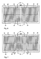
- the electrodes of the IDT halves 34 and 36, and the electrodes of the IDT halves 38 and 40 are displaced from the center of the SAW resonator and are positioned in spatial synchronism with the fingers of the reflection gratings 22 and 24.
- the resonant cavity is then reduced to a length Is between the IDT halves, which are differentially excited as described above via the balanced signal lines 42 and 52.
- the shorter cavity length also makes the resonator less sensitive to fabrication variations than the arrangement of Figs. 2 to 4.
- Figs. 2 and 6 can be combined, for example as shown in Fig. 7.
- the IDT halves 34 and 36 are arranged as described above with reference to Fig. 6, and the IDT halves 38 and 40 are arranged as described above with reference to Figs. 2 and 4.
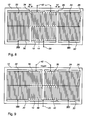
- the inner rail 26 is shown as being divided into two halves, but as already stated this need not be the case, and the inner rail 26 can be continuous over the entire length of the SAW resonator. In the latter case, the SAW resonator can also provide a balanced-to-unbalanced coupling, for example as described below with reference to Figs. 8 to 11.
- SAW resonator having unbalanced input and output signal connections.
- Such a SAW resonator may be particularly useful in circuits, such as oscillator circuits, which do not require balanced connections. Examples of such SAW resonators are illustrated in Figs. 12 and 13.
- IDT halves 38 and 40 are referred to above and illustrated in Figs. 9, 11, and 13, and IDT halves 34 and 36 are referred to above and illustrated in Figs. 12 and 13, the electrodes of the IDTs providing an unbalanced signal connection could more generally be divided into two groups of unequal size, with the resonant cavity between the two groups.
- SAW resonators which may use surface skimming bulk waves rather than surface acoustic waves.
- Two or more SAW resonators may be connected in tandem, as is known in the art, in order to provide desired response characteristics, such resonators being provided either on separate substrates or on a single substrate with a desired separation between them.
- the fingers of the reflection gratings 22 and 24 can have a pitch different from that of the IDT electrodes, and as is known in the art the reflection gratings could be constituted by grooves in the substrate instead of fingers on the substrate, or could be dispensed with entirely if the IDTs are sufficiently long to provide adequate coupling between them.
- different sizes of the resonant cavities may be provided, and other parameters of the resonators may similarly be changed to suit particular requirements.
Landscapes
- Physics & Mathematics (AREA)
- Acoustics & Sound (AREA)
- Surface Acoustic Wave Elements And Circuit Networks Thereof (AREA)
Claims (15)
- Oberflächenwellen-Resonator mit:dadurch gekennzeichnet, daß zumindest einer der IDT's und seine äußere Schiene in zwei eine entgegengesetzte Phase aufweisende Hälften (34,44;36,46) unterteilt ist.einem piezoelektrischen Substrat (10) undzwei IDT's (interdigitale Wandler) (34,36;38,40), die Seite an Seite auf einer Oberfläche des Substrats mit einer gemeinsamen Schiene (26) zwischen diesen derart angeordnet sind, daß Oberflächenwellen zwischen den IDT's gekoppelt werden, wobei jeder IDT ineinander verschachtelte Elektroden aufweist, die sich von der gemeinsamen Schiene und von einer jeweiligen äußeren Schiene (44,46;48,50) aus erstrecken, wobei die äußeren Schienen Signalverbindungen an den Resonator ergeben,
- Oberflächenwellen-Resonator nach Anspruch 1,
bei dem jeder der IDT's und dessen zugehörige äußere Schiene in zwei eine entgegengesetzte Phase aufweisende Hälften (34,44;36,46;38,48;40,50)unterteilt ist. - Oberflächenwellen-Resonator nach Anspruch 2,
bei dem die gemeinsame Schiene (26) in zwei Hälften unterteilt ist. - Oberflächenwellen-Resonator nach Anspruch 1,
bei dem lediglich einer der IDT's und dessen äußere Schiene in zwei eine entgegengesetzte Phase aufweisende Hälften unterteilt ist, und bei dem die äußere Schiene (19) des anderen IDT (14) und die gemeinsame Schiene (26) einen unsymmetrischen Signalanschluß (20) an den Resonator ergeben. - Oberflächenwellen-Resonator nach einem der Ansprüche 1 bis 4, der Reflexionsgitter (22,24), zwischen denen die beiden IDT's angeordnet sind, einschließt, um einen Resonanzhohlraum für jeden IDT zu bilden.
- Oberflächenwellen-Resonator nach Anspruch 5,
bei dem jeder IDT einen Abstand von ungefähr 0,625λ+nλ/2 von einem benachbarten Reflexionsgitter aufweist, worin λ eine Wellenlänge einer Oberflächenwelle ist, die sich ausbreiten soll, und n gleich Null oder eine positive ganze Zahl ist. - Oberflächenwellen-Resonator nach Anspruch 5 oder 6,
bei dem die beiden IDT's unterschiedliche Abstände von den Reflexionsgittern aufweisen. - Oberflächenwellen-Resonator nach Anspruch 5,
bei dem Elektroden von zumindest einem der IDT's in räumlich synchroner Beziehung mit benachbarten Fingern der Reflexionsgitter angeordnet sind. - Oberflächenwellen-Resonator nach Anspruch 8,
bei dem Elektroden jedes der IDT's in räumlich synchroner Beziehung mit benachbarten Fingern der Reflexionsgitter angeordnet sind. - Oberflächenwellen-Resonator nach Anspruch 9,
bei dem die Resonanzhohlräume der beiden IDT's unterschiedliche Längen aufweisen. - Oberflächenwellen-Resonator nach Anspruch 8, 9 oder 10, bei dem der Resonanzhohlraum für jeden IDT, dessen Elektroden in räumlich synchroner Beziehung mit benachbarten Fingern der Reflexionsgitter angeordnet sind, eine Länge von ungefähr 0,4375λ+nλ/2 aufweist, worin λ eine Wellenlänge einer Oberflächenwelle ist, die sich ausbreiten soll, und n gleich Null oder eine positive ganze Zahl ist.
- Oberflächenwellen-Resonator mit zwei Moden, mit zwei IDT's (interdigitale Wandler) (34,36;14), die Seite an Seite zwischen Reflexionsgittern (22,24) auf einer Oberfläche eines piezoelektrischen Substrates (10) angordnet sind, um eine Kopplung von Oberflächenwellen zwischen diesen zu erzielen, wobei jeder IDT ineinander verschachtelte Elektroden aufweist, die sich von einer gemeinsamen Schiene (26) zwischen den beiden IDT's und von einer jeweiligen äußeren Schiene (16,19) des IDT aus erstrecken,
dadurch gekennzeichnet, daß die Elektroden von zumindest einem der IDT's in zwei eine entgegengesetzte Phase aufweisende Gruppen (34,36) mit einem Resonanzhohlraum zwischen den Gruppen unterteilt sind, und daß die Elektroden jeder Gruppe (34,36) in räumlich synchroner Beziehung zu benachbarten Fingern des benachbarten Reflexionsgitters (22,24) angeordnet sind. - Oberflächenwellen-Resonator nach Anspruch 12,
bei dem die Elektroden jedes der IDT's in zwei eine entgegengesetzte Phase aufweisende Gruppen (34,36;38,40) mit einem Resonanzhohlraum zwischen den Gruppen unterteilt sind, und bei dem die Elektroden jeder Gruppe in räumlich synchroner Beziehung zu benachbarten Fingern des benachbarten Reflexionsgitters angeordnet sind. - Oberflächenwellen-Resonator nach Anspruch 13,
bei dem die Resonanzhohlräume der beiden IDT's unterschiedliche Längen aufweisen. - Oberflächenwellen-Resonator nach Anspruch 12,13 oder 14, bei dem der Resonanzhohlraum für jeden IDT, dessen Elektroden in räumlich synchroner Beziehung zu benachbarten Fingern der Reflexionsgitter angeordnet sind, eine Länge von ungefähr 0,4375λ+nλ/2 aufweist, worin λ eine Wellenlänge einer Oberflächenwelle ist, die sich ausbreiten soll, und n gleich Null oder eine positive ganze Zahl ist.
Applications Claiming Priority (3)
| Application Number | Priority Date | Filing Date | Title |
|---|---|---|---|
| US160628 | 1993-12-02 | ||
| US08/160,628 US5365138A (en) | 1993-12-02 | 1993-12-02 | Double mode surface wave resonators |
| PCT/CA1994/000345 WO1995015614A1 (en) | 1993-12-02 | 1994-06-22 | Double mode surface wave resonators |
Publications (2)
| Publication Number | Publication Date |
|---|---|
| EP0733282A1 EP0733282A1 (de) | 1996-09-25 |
| EP0733282B1 true EP0733282B1 (de) | 1998-10-07 |
Family
ID=22577692
Family Applications (1)
| Application Number | Title | Priority Date | Filing Date |
|---|---|---|---|
| EP94919535A Expired - Lifetime EP0733282B1 (de) | 1993-12-02 | 1994-06-22 | Oberflächenwellenresonatoren mit zwei moden |
Country Status (9)
| Country | Link |
|---|---|
| US (1) | US5365138A (de) |
| EP (1) | EP0733282B1 (de) |
| JP (1) | JP3060070B2 (de) |
| KR (1) | KR0175522B1 (de) |
| CN (1) | CN1075288C (de) |
| AU (1) | AU678903B2 (de) |
| CA (1) | CA2135983C (de) |
| DE (1) | DE69413843T2 (de) |
| WO (1) | WO1995015614A1 (de) |
Families Citing this family (39)
| Publication number | Priority date | Publication date | Assignee | Title |
|---|---|---|---|---|
| DE69424737T2 (de) * | 1993-10-08 | 2000-09-28 | Matsushita Electric Ind Co Ltd | Akustisches Oberflächenwellenfilter |
| US5448125A (en) * | 1994-06-27 | 1995-09-05 | E. I. Du Pont De Nemours And Company | Surface skimming bulk wave generation in KTiOPO4 and its analogs |
| JP3244386B2 (ja) * | 1994-08-23 | 2002-01-07 | 松下電器産業株式会社 | 弾性表面波装置 |
| JP3185591B2 (ja) * | 1995-03-03 | 2001-07-11 | 株式会社村田製作所 | Saw共振子 |
| US5835990A (en) * | 1995-06-16 | 1998-11-10 | Northern Telecom Limited | Longitudinally coupled double mode surface wave resonators |
| FR2739232B1 (fr) * | 1995-09-26 | 1997-10-24 | Thomson Csf | Filtre a ondes acoustiques de surface utilisant le couplage de trois voies acoustiques |
| GB2306821B (en) * | 1995-11-03 | 2000-05-31 | Advanced Saw Prod Sa | Electro-acoustic device |
| US5668431A (en) * | 1996-03-07 | 1997-09-16 | Northern Telecom Limited | Surface wave devices for differential coherent detectors |
| US6745627B1 (en) | 1996-05-21 | 2004-06-08 | Honeywell International Inc. | Electrostatic drive for accelerometer |
| US5948981A (en) * | 1996-05-21 | 1999-09-07 | Alliedsignal Inc. | Vibrating beam accelerometer |
| EP0921636B1 (de) * | 1996-05-23 | 2007-04-04 | Matsushita Electric Industrial Co., Ltd. | Akustisches Oberflächenwellenfilter und mehrstufiges akustisches Oberflächenwellenfilter |
| JP3180055B2 (ja) | 1996-05-23 | 2001-06-25 | 松下電器産業株式会社 | 弾性表面波フィルタ及び多段弾性表面波フィルタ |
| US6348845B2 (en) | 1996-05-23 | 2002-02-19 | Matsushita Electric Industrial Co., Ltd. | Surface acoustic wave filter and multistage surface acoustic wave filter |
| US6801100B2 (en) * | 1996-05-23 | 2004-10-05 | Matsushita Electric Industrial Co., Ltd. | Inter-digital transducer, surface acoustic wave filter and communication apparatus using the same |
| JP3239064B2 (ja) * | 1996-05-28 | 2001-12-17 | 富士通株式会社 | 弾性表面波装置 |
| US5793266A (en) * | 1996-08-12 | 1998-08-11 | Motorola Inc. | Differential input and/or differential output, transversely-coupled surface acoustic wave filter |
| JP3186604B2 (ja) * | 1996-10-09 | 2001-07-11 | 株式会社村田製作所 | 弾性表面波フィルタ装置 |
| CA2199238C (en) * | 1997-03-05 | 2002-07-02 | Ji-Dong Dai | Surface wave device with capacitance |
| FR2762458B1 (fr) * | 1997-04-18 | 1999-07-09 | Thomson Csf | Dispositif a ondes acoustiques de surface a couplage par proximite a entrees/sorties differentielles |
| US5896071A (en) * | 1997-05-15 | 1999-04-20 | Northern Telecom Limited | Surface wave device balun resonator filters |
| DE19722859C1 (de) * | 1997-05-31 | 1998-10-15 | Dresden Ev Inst Festkoerper | Oberflächenwellenresonator |
| JP3154402B2 (ja) * | 1997-11-12 | 2001-04-09 | 日本電気株式会社 | Sawフィルタ |
| JP3137064B2 (ja) * | 1998-01-16 | 2001-02-19 | 日本電気株式会社 | 弾性表面波フィルタ |
| US5948982A (en) * | 1998-02-23 | 1999-09-07 | Alliedsignal Inc. | Vibrating beam accelerometers and methods of forming vibrating beam accelerometers |
| JP3469806B2 (ja) * | 1998-05-13 | 2003-11-25 | 三洋電機株式会社 | 弾性表面波フィルタ |
| JP4336931B2 (ja) * | 1999-12-28 | 2009-09-30 | 日立金属株式会社 | 高周波スイッチモジュール |
| DE10007178A1 (de) * | 2000-02-17 | 2001-08-23 | Epcos Ag | Oberflächenwellenfilter mit Reaktanzelementen |
| JP3391347B2 (ja) * | 2000-06-26 | 2003-03-31 | 株式会社村田製作所 | 縦結合共振子型弾性表面波フィルタ |
| CN100547919C (zh) * | 2005-03-28 | 2009-10-07 | 京瓷株式会社 | 弹性表面波共振子以及通信装置 |
| US7453335B2 (en) * | 2005-03-28 | 2008-11-18 | Kyocera Corporation | Surface acoustic wave resonator, surface acoustic wave filter and surface acoustic wave duplexer, and communications equipment |
| JP4537254B2 (ja) * | 2005-04-28 | 2010-09-01 | 富士通メディアデバイス株式会社 | 弾性表面波フィルタおよび分波器 |
| CN101316099B (zh) * | 2008-07-04 | 2010-06-16 | 无锡市好达电子有限公司 | 双通道声表面波滤波器 |
| US9083300B2 (en) * | 2010-09-01 | 2015-07-14 | Qualcomm Mems Technologies, Inc. | Electromechanical systems piezoelectric contour mode differential resonators and filters |
| CN103152011B (zh) * | 2013-03-14 | 2016-08-24 | 北京中讯四方科技股份有限公司 | 一种基于多相位倒相横向平衡式结构的声表面波滤波器 |
| CN106797208B (zh) * | 2015-01-16 | 2020-03-20 | 株式会社村田制作所 | 谐振器 |
| RU2633658C2 (ru) * | 2016-03-09 | 2017-10-16 | Акционерное общество "Научно-производственное предприятие "Радар ммс" | Резонатор на поверхностных акустических волнах |
| CN112511124A (zh) * | 2021-02-07 | 2021-03-16 | 成都频岢微电子有限公司 | 用于改善dms型接收滤波器带外抑制的接地结构及滤波器 |
| CN114204914B (zh) * | 2022-02-21 | 2022-06-14 | 中国电子科技集团公司信息科学研究院 | 一种用于气体检测的声表面波横向耦合谐振器 |
| CN119363068A (zh) * | 2024-12-26 | 2025-01-24 | 天通瑞宏科技有限公司 | 高功率容量的dms滤波器和通信设备 |
Family Cites Families (4)
| Publication number | Priority date | Publication date | Assignee | Title |
|---|---|---|---|---|
| JPS57119509A (en) * | 1981-01-19 | 1982-07-26 | Toshiba Corp | Surface acoustic wave resonator |
| USRE33957E (en) * | 1982-07-26 | 1992-06-09 | Toyo Communication Equipment Co., Ltd. | High frequency narrow-band multi-mode filter |
| JPS59131213A (ja) * | 1982-07-26 | 1984-07-28 | Toyo Commun Equip Co Ltd | 高周波狭帯域多重モ−ド・フイルタ |
| US5223762A (en) * | 1990-12-27 | 1993-06-29 | Murata Manufacturing Co., Ltd. | Surface acoustic wave filter |
-
1993
- 1993-12-02 US US08/160,628 patent/US5365138A/en not_active Expired - Lifetime
-
1994
- 1994-06-22 AU AU21853/95A patent/AU678903B2/en not_active Ceased
- 1994-06-22 JP JP7515305A patent/JP3060070B2/ja not_active Expired - Fee Related
- 1994-06-22 EP EP94919535A patent/EP0733282B1/de not_active Expired - Lifetime
- 1994-06-22 KR KR1019960702889A patent/KR0175522B1/ko not_active Expired - Lifetime
- 1994-06-22 CN CN94194848A patent/CN1075288C/zh not_active Expired - Fee Related
- 1994-06-22 DE DE69413843T patent/DE69413843T2/de not_active Expired - Fee Related
- 1994-06-22 WO PCT/CA1994/000345 patent/WO1995015614A1/en not_active Ceased
- 1994-11-16 CA CA002135983A patent/CA2135983C/en not_active Expired - Fee Related
Also Published As
| Publication number | Publication date |
|---|---|
| CA2135983A1 (en) | 1995-06-03 |
| EP0733282A1 (de) | 1996-09-25 |
| KR960706715A (ko) | 1996-12-09 |
| CA2135983C (en) | 1998-02-10 |
| CN1075288C (zh) | 2001-11-21 |
| JPH09505706A (ja) | 1997-06-03 |
| DE69413843T2 (de) | 1999-03-04 |
| JP3060070B2 (ja) | 2000-07-04 |
| WO1995015614A1 (en) | 1995-06-08 |
| KR0175522B1 (ko) | 1999-04-01 |
| US5365138A (en) | 1994-11-15 |
| AU2185395A (en) | 1995-06-19 |
| CN1141697A (zh) | 1997-01-29 |
| AU678903B2 (en) | 1997-06-12 |
| DE69413843D1 (de) | 1998-11-12 |
Similar Documents
| Publication | Publication Date | Title |
|---|---|---|
| EP0733282B1 (de) | Oberflächenwellenresonatoren mit zwei moden | |
| US5835990A (en) | Longitudinally coupled double mode surface wave resonators | |
| EP0897218B1 (de) | Akustische Oberflächenwellenfilter | |
| EP0652637B1 (de) | Akustisches Oberflächenwellenfilter | |
| KR100196292B1 (ko) | 표면 음향파 필터 | |
| EP0648015B1 (de) | Akustisches Oberflächenwellenfilter | |
| EP0718970B1 (de) | Akustisches Oberflächenwellenfilter | |
| US6556100B2 (en) | Surface acoustic wave filter with a passband formed by a longitudinally coupled filter and a resonator inductance | |
| US4542356A (en) | High frequency narrow-band multi-mode filter | |
| US5646584A (en) | Saw filter including electrodes of opposing polarity | |
| US5874868A (en) | Longitudinally coupled surface acoustic wave resonator filter having different distances between transducers | |
| US20010011932A1 (en) | Surface acoustic wave filter | |
| EP1005153B1 (de) | Akustisches Oberflächenwellenfilter | |
| CN1084086C (zh) | 表面声波滤波器 | |
| EP0981857B1 (de) | Oberflächenwellen balun resonatorfilter | |
| US5604393A (en) | Surface acoustic wave device | |
| EP1397861B1 (de) | Oberflächenwellenfilteranornung und kommunikationsgerät mit derselben | |
| CA2199238C (en) | Surface wave device with capacitance | |
| EP0637873B1 (de) | Akustisches Oberflächenwellenfilter | |
| USRE33957E (en) | High frequency narrow-band multi-mode filter | |
| US7425882B2 (en) | Balanced-type surface acoustic wave filter | |
| EP0100503B1 (de) | Hochfrequentes Multimodefilter mit schmalem Durchlassband | |
| JP3654920B2 (ja) | 多段接続弾性表面波多重モードフィルタ | |
| KR100638889B1 (ko) | 표면 탄성파 필터 | |
| JP3835872B2 (ja) | 弾性表面波共振子 |
Legal Events
| Date | Code | Title | Description |
|---|---|---|---|
| PUAI | Public reference made under article 153(3) epc to a published international application that has entered the european phase |
Free format text: ORIGINAL CODE: 0009012 |
|
| 17P | Request for examination filed |
Effective date: 19960603 |
|
| AK | Designated contracting states |
Kind code of ref document: A1 Designated state(s): CH DE FR GB IT LI NL SE |
|
| 17Q | First examination report despatched |
Effective date: 19961024 |
|
| GRAG | Despatch of communication of intention to grant |
Free format text: ORIGINAL CODE: EPIDOS AGRA |
|
| GRAG | Despatch of communication of intention to grant |
Free format text: ORIGINAL CODE: EPIDOS AGRA |
|
| GRAG | Despatch of communication of intention to grant |
Free format text: ORIGINAL CODE: EPIDOS AGRA |
|
| GRAH | Despatch of communication of intention to grant a patent |
Free format text: ORIGINAL CODE: EPIDOS IGRA |
|
| GRAH | Despatch of communication of intention to grant a patent |
Free format text: ORIGINAL CODE: EPIDOS IGRA |
|
| GRAA | (expected) grant |
Free format text: ORIGINAL CODE: 0009210 |
|
| AK | Designated contracting states |
Kind code of ref document: B1 Designated state(s): CH DE FR GB IT LI NL SE |
|
| REG | Reference to a national code |
Ref country code: CH Ref legal event code: NV Representative=s name: JOHN P. MUNZINGER INGENIEUR-CONSEIL Ref country code: CH Ref legal event code: EP |
|
| REF | Corresponds to: |
Ref document number: 69413843 Country of ref document: DE Date of ref document: 19981112 |
|
| ET | Fr: translation filed | ||
| RAP4 | Party data changed (patent owner data changed or rights of a patent transferred) |
Owner name: NORTEL NETWORKS CORPORATION |
|
| PLBE | No opposition filed within time limit |
Free format text: ORIGINAL CODE: 0009261 |
|
| STAA | Information on the status of an ep patent application or granted ep patent |
Free format text: STATUS: NO OPPOSITION FILED WITHIN TIME LIMIT |
|
| 26N | No opposition filed | ||
| REG | Reference to a national code |
Ref country code: GB Ref legal event code: IF02 |
|
| REG | Reference to a national code |
Ref country code: CH Ref legal event code: PFA Free format text: NORTEL NETWORKS CORPORATION TRANSFER- NORTEL NETWORKS LIMITED * NORTHERN TELECOM LIMITED TRANSFER- NORTEL NETWORKS CORPORATION Ref country code: CH Ref legal event code: NV Representative=s name: CRONIN INTELLECTUAL PROPERTY |
|
| PGFP | Annual fee paid to national office [announced via postgrant information from national office to epo] |
Ref country code: SE Payment date: 20030526 Year of fee payment: 10 |
|
| PGFP | Annual fee paid to national office [announced via postgrant information from national office to epo] |
Ref country code: NL Payment date: 20030528 Year of fee payment: 10 |
|
| PGFP | Annual fee paid to national office [announced via postgrant information from national office to epo] |
Ref country code: CH Payment date: 20030826 Year of fee payment: 10 |
|
| REG | Reference to a national code |
Ref country code: FR Ref legal event code: CD |
|
| PGFP | Annual fee paid to national office [announced via postgrant information from national office to epo] |
Ref country code: GB Payment date: 20040528 Year of fee payment: 11 |
|
| PGFP | Annual fee paid to national office [announced via postgrant information from national office to epo] |
Ref country code: FR Payment date: 20040602 Year of fee payment: 11 |
|
| PG25 | Lapsed in a contracting state [announced via postgrant information from national office to epo] |
Ref country code: SE Free format text: LAPSE BECAUSE OF NON-PAYMENT OF DUE FEES Effective date: 20040623 |
|
| PG25 | Lapsed in a contracting state [announced via postgrant information from national office to epo] |
Ref country code: LI Free format text: LAPSE BECAUSE OF NON-PAYMENT OF DUE FEES Effective date: 20040630 Ref country code: CH Free format text: LAPSE BECAUSE OF NON-PAYMENT OF DUE FEES Effective date: 20040630 |
|
| PGFP | Annual fee paid to national office [announced via postgrant information from national office to epo] |
Ref country code: DE Payment date: 20040630 Year of fee payment: 11 |
|
| PG25 | Lapsed in a contracting state [announced via postgrant information from national office to epo] |
Ref country code: NL Free format text: LAPSE BECAUSE OF NON-PAYMENT OF DUE FEES Effective date: 20050101 |
|
| EUG | Se: european patent has lapsed | ||
| EUG | Se: european patent has lapsed | ||
| REG | Reference to a national code |
Ref country code: CH Ref legal event code: PL |
|
| NLV4 | Nl: lapsed or anulled due to non-payment of the annual fee |
Effective date: 20050101 |
|
| PG25 | Lapsed in a contracting state [announced via postgrant information from national office to epo] |
Ref country code: IT Free format text: LAPSE BECAUSE OF NON-PAYMENT OF DUE FEES Effective date: 20050622 Ref country code: GB Free format text: LAPSE BECAUSE OF NON-PAYMENT OF DUE FEES Effective date: 20050622 |
|
| PG25 | Lapsed in a contracting state [announced via postgrant information from national office to epo] |
Ref country code: DE Free format text: LAPSE BECAUSE OF NON-PAYMENT OF DUE FEES Effective date: 20060103 |
|
| PG25 | Lapsed in a contracting state [announced via postgrant information from national office to epo] |
Ref country code: FR Free format text: LAPSE BECAUSE OF NON-PAYMENT OF DUE FEES Effective date: 20060228 |
|
| GBPC | Gb: european patent ceased through non-payment of renewal fee |
Effective date: 20050622 |
|
| REG | Reference to a national code |
Ref country code: FR Ref legal event code: ST Effective date: 20060228 |