EP0726596A2 - Plasmaätzmethode - Google Patents
Plasmaätzmethode Download PDFInfo
- Publication number
- EP0726596A2 EP0726596A2 EP96101751A EP96101751A EP0726596A2 EP 0726596 A2 EP0726596 A2 EP 0726596A2 EP 96101751 A EP96101751 A EP 96101751A EP 96101751 A EP96101751 A EP 96101751A EP 0726596 A2 EP0726596 A2 EP 0726596A2
- Authority
- EP
- European Patent Office
- Prior art keywords
- layer
- processing gas
- etching
- processing
- discharge duration
- Prior art date
- Legal status (The legal status is an assumption and is not a legal conclusion. Google has not performed a legal analysis and makes no representation as to the accuracy of the status listed.)
- Granted
Links
Images


Classifications
-
- H—ELECTRICITY
- H10—SEMICONDUCTOR DEVICES; ELECTRIC SOLID-STATE DEVICES NOT OTHERWISE PROVIDED FOR
- H10P—GENERIC PROCESSES OR APPARATUS FOR THE MANUFACTURE OR TREATMENT OF DEVICES COVERED BY CLASS H10
- H10P50/00—Etching of wafers, substrates or parts of devices
-
- H—ELECTRICITY
- H10—SEMICONDUCTOR DEVICES; ELECTRIC SOLID-STATE DEVICES NOT OTHERWISE PROVIDED FOR
- H10P—GENERIC PROCESSES OR APPARATUS FOR THE MANUFACTURE OR TREATMENT OF DEVICES COVERED BY CLASS H10
- H10P50/00—Etching of wafers, substrates or parts of devices
- H10P50/20—Dry etching; Plasma etching; Reactive-ion etching
- H10P50/28—Dry etching; Plasma etching; Reactive-ion etching of insulating materials
- H10P50/282—Dry etching; Plasma etching; Reactive-ion etching of insulating materials of inorganic materials
- H10P50/283—Dry etching; Plasma etching; Reactive-ion etching of insulating materials of inorganic materials by chemical means
Definitions
- the present invention relates to a plasma etching method and, more particularly, to a method of etching an SiO 2 layer at a high selection ratio relative to an SiN layer.
- etching for forming a desired fine pattern on a thin film stacked on a wafer is used.
- a dry etching method of performing etching in a plasma atmosphere is used.
- a gas mixture including H 2 such as CF 4 + H 2 gas, or a gas mixture of a CH x F y -based gas having H bonds and CO 2 or CO gas such as CH 2 F 2 + CO 2 gas or CHF 3 + CO gas is used as an etching gas.
- the selection ratio of an etching target layer to be etched to an underlayer therebelow i.e., the ratio of the etching rate of the etching target layer to that of the underlayer be as high as possible.
- the selection ratio can he increased to 10 or more higher than that using a single CH x F y -based gas.
- a so-called self-alignment method As a technique of forming a semiconductor device with a high dimensional accuracy, a so-called self-alignment method is known.
- contact holes are formed in an insulating interlayer along a gate electrode, using the gate electrode, covered with a protection film, itself as a mask pattern.
- typical materials for the insulating interlayer and the protective insulating film are SiO 2 and SiN, respectively.
- an SiO 2 insulating interlayer is etched (to be described later with reference to FIG. 7).
- a shoulder or corner portion 5a of the SiN insulating film is etched from two directions, i.e., from the upper and lateral directions, so that the corner portion is more easily eroded.
- the etching selection ratio decreases at the corner portion 5a even under a condition for assuring a sufficiently high etching selection ratio (SiO 2 /SiN) at a flat portion 5b.
- the decrease in etching selection ratio generates openings in the SiN insulating film to cause problems such as short-circuiting of the gate electrode upon completion of the device.
- the selection ratios also decrease at corner portions, or shoulder portions of not only an SiN underlayer but also an underlayer consisting of Si, Al, TiN, TiSi, W, WSi, or the like.
- a plasma etching method in which a processing gas is introduced into a processing room housing a substrate, an RF power is applied across opposite electrodes to cause the processing gas to discharge, thereby generating a plasma, and a first layer supported by the substrate is etched by using the plasma in preference to a second layer supported by the substrate and consisting of a material different from that of the first layer, wherein the first layer consists essentially of SiO 2 while second layer consists essentially of a material selected from a group consisting of SiN, Si, Al, and TiN, the processing gas contains C 4 F 8 and CO, and progress of dissociation of C 4 F 8 is controlled, using a discharge duration of each part of the processing gas as a parameter, in order to set an etching selection ratio of the first layer to the second layer.
- a plasma etching method in which a processing gas is introduced into a processing room housing a substrate, an RF power is applied across opposite electrodes to cause the processing gas to discharge, thereby generating a plasma, and a first layer supported by the substrate is etched by using the plasma in preference to a second layer supported by the substrate and consisting of a material different from that of the first layer, wherein the first layer consists essentially of SiO 2 while the second layer consists essentially of a material selected from a group consisting of SiN, Si, Al, TiN, W, WSi, and TiSi, the processing gas contains C 4 F 8 and CO, and a density ratio of C 2 F 4 and CF 3 , which are generated upon dissociation of C 4 F 8 , is controlled, using a discharge duration of each part of the processing gas as a parameter, in order to set an etching selection ratio of the first layer to the second layer.
- a plasma etching method using a plasma etching apparatus in which a first layer supported by a substrate is etched in preference to a second layer supported by the substrate and consisting of a material different from that of the first layer, wherein the apparatus comprises a first electrode for supporting the substrate in a processing room, a second electrode opposite to the first electrode in the processing room, and an RF power supply for applying an RF power across the first and second electrodes, and wherein the first layer consists essentially of SiO 2 while the second layer consists essentially of a material selected from a group consisting of SiN, Si, Al, TiN, W, WSi, and TiSi, the processing gas contains C 4 F 8 and CO, the method comprising the steps of: selecting a value for a discharge duration of each part of a processing gas as a parameter in order to set an etching selection ratio of the first layer to the second layer, a density ratio of C 2 F 4 to CF 3 , which are generated upon
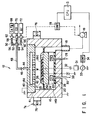
- a dipole ring type magnetron plasma etching apparatus 12 shown in FIG. 1 has an airtight processing chamber 16 consisting of, e.g., aluminum.
- a susceptor support base 22 consisting of, e.g., aluminum is disposed at the center of the bottom portion in the processing chamber 16 through an insulating plate 20 consisting of, e.g., ceramic.
- a susceptor 24 is disposed as a lower electrode consisting of, e.g., aluminum on the support base 22.
- An exhaust ring 25 consisting of, e.g., aluminum is disposed around the susceptor 24.
- the interior of the processing chamber 16 is partitioned by the susceptor 24 and the exhaust ring 25 into an upper processing room, i.e., a discharge room 14a, and a lower auxiliary room 14b.
- a large number of holes 25a are formed in the exhaust ring 25 at an equal interval to cause the discharge room 14a to communicate with the auxiliary room 14b.
- An exhaust pipe 18 in which a vacuum pump 19 having a controllable exhaust amount is interposed is connected to the bottom portion of the processing chamber 16.
- the interior of the processing room 14a is uniformly evacuated by the vacuum pump 19 through the auxiliary room 14b.
- the capacity of the discharge room 14a is set to, e.g., about 3.5 liters.
- a room 26 for introducing a cold or heat medium is formed in the susceptor support base 22.
- a medium feed pipe 28 and a medium exhaust pipe 30 which extend through the bottom portion of the processing chamber 16 are connected to the room 26.
- An electrostatic chuck 36 for attracting and chucking a semiconductor wafer W serving as a target object is disposed on the upper surface of the susceptor 24.
- the electrostatic chuck 36 is constituted by, e.g., a copper foil 36a and polyimide films which interpose the copper foil 36a.
- a high-voltage DC power supply 38 is connected to the copper foil 36a. When an DC voltage is applied to the copper foil 36a, the wafer W is chucked by a Coulomb force to the surface of the chuck 36.
- the focus ring 17 facilitates etching to be uniformly performed at every part on the wafer W.
- the thick focus ring 17 and the thick electrostatic chuck 36 are illustrated in FIG. 1, they are as thin as the wafer W in practice.
- An RF power supply 33 of, e.g., 13.56 MHz for generating plasma is connected to the susceptor 24 through a matching circuit 31 and a blocking capacitor 32.
- the output from the RF power supply 33 is adjusted by an output control section 34 connected to a CPU 13. Under the control of the control section 34, an RF power is applied continuously or in pulsation from the RF power supply 33 to the susceptor 24 (to be described later).
- the ceiling portion of the processing chamber 16 is defined by an upper electrode 40.
- a portion between the side wall and ceiling portion of the processing chamber 16 are sealed by a seal member 41 constituted by, e.g., an O-ring.
- the upper electrode 40, the side wall of the processing chamber 16, and the exhaust ring 25 are grounded. Therefore, when an RF power is applied to the susceptor 24 to form an RF electric field in the processing room 14a, the susceptor 24 functions as a cathode electrode, and the members 40, 16, and 25 function as an anode electrode.
- the upper electrode 40 consists of a conductive material such as amorphous carbon, SiC, or Al.
- the upper electrode 40 has a shower head structure. More specifically, the upper electrode 40 has a hollow interior, and a large number of gas diffusion holes 42 are formed in its entire surface opposite to the wafer W.
- a dispensing plate (not shown) is disposed in the upper electrode 40. An etching gas fed into the upper electrode 40 through a gas feed pipe 44 is uniformly sprayed into the processing chamber 16 through the gas diffusion holes 42.
- a gas supply pipe 48 in which a valve 46 is interposed is connected to the gas feed pipe 44.
- the distal end of the gas supply pipe 48 is branched into three branch pipes 50, 52, and 54.
- Gas sources 68, 70, and 72 for different gases are connected to the branch pipes 50, 52, and 54 through valves 56, 58, and 60, and massflow controllers 62, 64, and 66 for controlling the flow rates, respectively.
- the gas sources 68, 70, and 72 are filled with C 4 F 8 , CO, and Ar gases, respectively. Further, N 2 and O 2 gases, and the like may be added to a processing gas.
- the flow rates of the massflow controllers 62, 64, and 66 are controlled by a control section 78 constituted by, e.g., a microcomputer connected to the CPU 13.
- the control section 78 also controls the exhaust amount of the vacuum pump 19.
- a ring-like dipole ring 74 is disposed around the outer side wall of the processing chamber 16 at a slight interval.
- the dipole ring 74 can be rotated by a driving member (not shown) in the circumferential direction at, e.g., 20 rpm.
- the dipole ring 74 is constituted by a large number of small permanent magnet pieces 76 which are coupled to each other in a ring shape, as shown in FIG. 2.
- the magnet pieces 76 are arrayed such that the magnetizing direction (indicated by arrows in the magnet pieces 76) turns twice around the ring 74.
- a pair of magnet pieces 76 which oppose each other about the center of the ring 74 have the same magnetizing direction.
- arrows illustrated on the wafer W indicate the directions of magnetic fields, and curves on the wafer W indicate the magnetic lines of constant force.
- the magnetic field on the wafer W is parallel to the target surface of the wafer W, and its magnetic force becomes stronger on point P2. For example, in this apparatus, a magnetic field having about 120G is generated.
- a method according to the present invention can be applied to a plasma etching apparatus of another type such as a bar magnet type magnetron plasma etching apparatus as shown in FIG. 3 as well as the dipole ring type magnetron etching apparatus as shown in FIG. 1.
- a bar magnet type magnetron plasma etching apparatus 82 shown in FIG. 3 has an N-S type permanent bar magnet 84 disposed above the upper electrode 40 serving as the ceiling portion of the processing chamber 16.
- the bar magnet 84 is rotated by a driving member (not shown) to form a magnetic field above and parallel to the surface of the wafer W in the processing chamber 16. Since the remaining portions are practically identical to those in the apparatus shown in FIG. 1, the same reference numerals denote the same parts, and a detailed description thereof will be omitted.
- FIGS. 1 and 3 A processing method in the magnetron plasma etching apparatuses shown in FIGS. 1 and 3 will be described below.
- the semiconductor wafer W serving as a target object is loaded into the processing chamber 16 from a load-lock room (not shown) connected to the processing chamber 16 through a gate valve (not shown).
- the wafer W is placed on the electrostatic chuck 36, and a DC voltage is applied to the electrostatic chuck 36 to attract and chuck the wafer W to the chuck 36.
- a processing gas i.e., a gas mixture of C 4 F 8 , CO, and Ar is supplied from the gas sources 68, 70, and 72 into the processing room 14a.
- the flow rate of the processing gas is controlled (to be described later). In this manner, the interior of the processing chamber 16 is kept at a predetermined processing pressure, e.g., 20 mTorr.
- an RF power is applied across the upper electrode 40 and the susceptor 24 serving as a lower electrode to convert the processing gas into a plasma.
- the processing gas is converted into a plasma and gradually dissociated to generate various radicals. These radicals etch an etching target layer on the surface of the wafer to form, e.g., a contact hole.
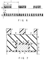
- FIG. 7 shows a manner of forming contact holes by self alignment.
- a gate electrode 4 is disposed on a substrate 1 through a gate insulating film 3.
- the gate electrode 4 is covered with an insulating film 5 consisting of SiN (silicon nitride).
- a thick SiO 2 insulating interlayer 6 is deposited on the gate structure.
- Contact holes 8 are formed by plasma-etching the insulating interlayer 6 at the two sides of the gate structure, using a patterned photoresist layer 7 as a mask, and C 4 F 8 /CO/Ar as a processing gas.
- a shoulder or corner portion 5a of the SiN insulating film 5 is etched from two directions, i.e., from the upper and lateral directions, so that the corner portion 5a is eroded more easily than the flat portion 5b of the insulating film 5. For this reason, the etching selection ratio is decreased at the shoulder portion or corner portion 5a even under a condition for assuring a sufficiently high etching selection ratio (SiO 2 /SiN) at the flat portion.
- the etching selection ratio (SiO 2 /SiN) is about 20 at the flat portion by using C 4 F 8 /CO/Ar as a processing gas without using the method of the present invention (to be described later).
- an etching selection ratio of 10 which is the target value of the present invention cannot be obtained.
- a decrease in etching selection ratio (SiO 2 /SiN) generates openings in the SiN insulating film 5 to cause problems such as short-circuiting of the gate electrode upon completion of the device.
- a thickness D1 of the gate structure including the SiN insulating film 5 is formed to be about 300 to 400 nm, and a thickness D2 of the SiN insulating film 5 is about 50 nm. Therefore, if an etching selection ratio (SiO 2 /SiN) of at least 10 is assured at the shoulder portion of the gate structure, i.e., the shoulder portion 5a of the SiN insulating film 5 serving as an underlayer, the SiN insulating film 5 remains 10 to 20 nm in thickness to obtain insulating properties.
- the selection ratio of an etching target layer (SiO 2 ) to its underlayer (SiN), and particularly the selection ratio at the corner portion or shoulder portion 5a of the underlayer (see FIG. 7) are set high. For this reason, the present inventors gave attention to the role of radicals which were obtained upon dissociation of a processing gas.
- an etching gas is dissociated according to the following formulas with an increase in application time (discharge duration).
- C 4 F 8 ⁇ CF 3 ⁇ CF 2 +F CF 2 +F ⁇ CF 3 In the generated radicals (including ions), the reaction of F with Si is promoted with a high content of F to decrease the etching selection ratio. More specifically, C 2 F 4 exhibits a relatively high etching selection ratio (SiO 2 /SiN), while radicals such as CF 3 and F exhibit low etching selection ratios. That is, to increase the etching selection ratio (SiO 2 /SiN), the C 2 F 4 content must be increased.
- CO is contained in a processing gas, and F generated upon dissociation is reacted with CO to decrease the F content in the radicals. Furthermore, by adjusting the time when the processing gas is converted in a plasma, the progress of dissociation of the processing gas is controlled.
- the residence time of a processing gas in the processing room i.e., the discharge room 14a is set to a predetermined value (e.g., 28 msec) or less with continuous application of an RF power.
- a predetermined value e.g. 28 msec
- the total flow rate (supply rate) of the processing gas and the exhaust capacity are controlled by the control section 78.
- Temperature management of a target object is important for performing processing for a high etching selection ratio (SiO 2 /SiN). Processing for a high etching selection ratio can be performed by heating the wafer W to 80°C to 150°C, and preferably to around 140°C (temperature of the surface to be processed).
- the control section 78 is set based on these parameters to control the supply rate of a processing gas and the exhaust rate.
- the discharge duration of the processing gas is shortened.
- the amount of radicals such as C 2 F 4 offering a high selection ratio is increased, while the amount of radicals such as CF 3 and F offering small selection ratios is decreased, thereby increasing the etching selection ratio at the corner portion or shoulder portion 5a of the underlayer.
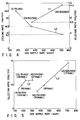
- FIG. 4 is a graph showing experimental results in the dipole ring type etching apparatus shown in FIG. 1.
- FIG. 5 is a graph for comparing the experimental results in the dipole ring type apparatus shown in FIG. 1 to those in the bar magnet type apparatus shown in FIG. 3.
- the etching pressure was set at 40 mTorr; the RF power, 1,700W; the temperatures of the ceiling portion and side wall of the processing chamber 16, 60°C; and the temperature of the susceptor 24, 20°C.
- the total supply rate of a processing gas and the exhaust rate were increased at a constant processing pressure and a constant composition ratio to decrease the residence time of the processing gas.
- a line L1 indicates the etching selection ratio (SiO 2 /SiN) at a shoulder portion with respect to the total supply rate of the processing gas
- a line L2 indicates the SiN etching rate at a flat portion with respect to the total supply rate of the processing gas.
- Figures in parentheses at each point indicate the flow rate (SCCM) of C 4 F 8 /CO/Ar processing gas.
- the selection ratio was 8.6 at a total supply rate of 360 SCCM, and abruptly increased to 14.5 at a total supply rate of 720 SCCM.
- the SiN etching rate decreased at the flat portion with an increase in total supply rate.
- a line L3 indicates the etching selection ratio (SiO 2 /SiN) at a shoulder portion in the dipole ring type apparatus shown in FIG. 1, which is obtained by drawing the line L1 in FIG. 4 without any change.
- a line L4 indicates the etching selection ratio (SiO 2 /SiN) at a shoulder portion in the bar magnet type apparatus shown in FIG. 3.
- Figures in upper parentheses at each point indicate the C 4 F 8 /CO/Ar flow rate (SCCM), as in FIG. 4, and figures in lower parentheses indicate the residence time (msec) of the processing gas in the processing room 14a.
- the selection ratio greatly increases from 8.6 to 14.5 with a decrease in residence time of the processing gas from 34 msec to 17 msec, as described above.
- the residence time is set to 28 msec or less with the target value of the etching selection ratio of 10 or more at the shoulder portion as a reference.
- the residence time is set to 46 msec or less on the basis of the target value of the etching section ratio of 10 or more at the shoulder portion.
- the processing pressure was set at 40 mTorr in the experiments related to FIGS. 4 and 5, the processing method according to the present invention can be applied at an etching pressure falling within a range equal to that of a normal etching pressure, e.g., within a range of several mTorr to several hundreds mTorr.
- the mixing ratio of C 4 F 8 , CO, and Ar gases was set at 1 : 15 : 20 in the dipole ring type apparatus, the processing method according to the present invention can be applied using a gas mixture having a mixing ratio of, e.g., about 1 : 2 : 0 to 1 : 30 : 40.
- the residence time of the processing gas is adjusted with continuous application of an RF voltage. For this reason, the supply rate of the processing gas and the exhaust amount of the processing room 14a are controlled by the control section 78.
- the application time of an RF voltage is taken into consideration as a parameter in addition to the residence time of the processing gas.
- the RF power supply 33 is controlled by the control section 34 to apply an RF voltage in pulsation and adjust the pulse width.
- FIG. 6 is a timing chart showing the mode of application pulses of an RF voltage for plasma generation.
- the residence time of a processing gas is set to, e.g., 28 msec or less, as shown in FIG. 5.
- the sum of pulse width times within the residence time of a processing gas is set to, e.g., 28 msec or less.
- a pulse does not mean an RF single wave but a set of continuous single waves, as shown in FIG. 6.
- the number of pulses existing in the residence time of a processing gas is set to one or more.
- FIG. 6 shows an example in which a single pulse having a pulse width t1 of 28 msec is applied within a long gas residence time T of more than 28 msec.
- the pulse width t1 is not limited to 28 msec and may be a smaller value.
- FIG. 6 shows an example in which 7 pulses each having a pulse width t2 of 4 msec are applied within the gas residence time T to obtain the total of 28-msec discharge duration.
- an RF voltage for plasma generation is applied in pulsation to set the discharge duration to a predetermined value, e.g., 28 msec or less, thereby increasing the content of radicals having a high selection ratio. Therefore, the selection ratio can be greatly increased at a shoulder portion.
- Temperature management of a target object is important for performing processing for a high etching selection ratio (SiO 2 /SiN). Processing for a high etching selection ratio can be performed by heating the wafer W to 80°C to 150°C, and preferably to about 140°C (temperature of the surface to be processed).
- a gas mixture containing C 4 F 8 and CO as etching gases, and Ar as an inert gas, is used. Even if a gas mixture containing only C 4 F 8 and CO is used instead of this, SiO 2 can be selectively etched with respect to SiN. Also in this case, the wafer W is heated to 80°C to 150°C, and preferably to about 140°C and kept at that temperature.
- a processing method of adjusting the CO amount in a processing gas or the temperature of a lower electrode to control the etching selection ratio will be described below.
- FIGS. 8 and 9 are graphs showing experimental results in the dipole ring type apparatus shown in FIG. 1.
- the etching pressure was set at 40 mTorr; the RF power, 1,700W; and the temperatures of the ceiling portion and side wall of the processing chamber 16, 60°C.
- the selection ratio at the shoulder portion is greatly increased, but that at the flat portion is slightly decreased. Therefore, the selection ratio at the shoulder portion can be further increased by increasing the temperature of the lower electrode to a certain degree, e.g., 20°C or more (the temperature of the target surface of the wafer W is 120°C or more at this time).
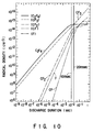
- FIG. 10 is a graph showing the results of a simulation of the relationship between the discharge duration (sec) and the density (cm -3 ) of radials produced by dissociation of C 4 F 8 . This simulation is based on a condition that an energy of 20 eV is applied to C 4 F 8 gas by discharge.
- etching selection ratio SiO 2 /SiN
- the density ratio of C 2 F 4 to CF 3 which are generated upon dissociation of C 4 F 8 can be controlled by changing the discharge duration. More specifically, to set the etching selection ratio of an SiO 2 layer serving as an etching target layer to an SiN layer serving as an underlayer, a preferable value is selected for the discharge duration of each part of a processing gas as a parameter. If a plurality of wafers W are continuously processed, a plasma etching apparatus is set in accordance with a selected parameter value before processing the lot of the wafers W. In general, selected parameter values are input, to the CPU 13 shown in FIG.
- the CPU 13 controls the control sections 34 and 78 so as to keep the input set values.
- an SiN underlayer has been exemplified in the above processing methods, the same effect can be obtained in the present invention even if an underlayer consists of another material such as Si, Al, TiN, W, WSi, or TiSi.
- Ar is used as a carrier gas for a processing gas, another inert gas such as He gas can be used instead of the Ar gas.
Landscapes
- Drying Of Semiconductors (AREA)
- ing And Chemical Polishing (AREA)
- Plasma Technology (AREA)
- Crystals, And After-Treatments Of Crystals (AREA)
Applications Claiming Priority (3)
| Application Number | Priority Date | Filing Date | Title |
|---|---|---|---|
| JP04353295A JP3778299B2 (ja) | 1995-02-07 | 1995-02-07 | プラズマエッチング方法 |
| JP43532/95 | 1995-02-07 | ||
| JP4353295 | 1995-02-07 |
Publications (3)
| Publication Number | Publication Date |
|---|---|
| EP0726596A2 true EP0726596A2 (de) | 1996-08-14 |
| EP0726596A3 EP0726596A3 (de) | 1997-10-29 |
| EP0726596B1 EP0726596B1 (de) | 2003-05-28 |
Family
ID=12666363
Family Applications (1)
| Application Number | Title | Priority Date | Filing Date |
|---|---|---|---|
| EP96101751A Expired - Lifetime EP0726596B1 (de) | 1995-02-07 | 1996-02-07 | Plasmaätzmethode |
Country Status (5)
| Country | Link |
|---|---|
| US (1) | US5595627A (de) |
| EP (1) | EP0726596B1 (de) |
| JP (1) | JP3778299B2 (de) |
| KR (1) | KR100214442B1 (de) |
| DE (1) | DE69628358T2 (de) |
Cited By (7)
| Publication number | Priority date | Publication date | Assignee | Title |
|---|---|---|---|---|
| EP0869545A3 (de) * | 1997-03-31 | 1999-05-26 | Applied Materials, Inc. | Selektives Plasmaätzen von Siliziumnitrid in Gegenwart von Silizium oder Siliziumoxyden unter Verwendung von Gemischen von (CH3F oder CH2F2) und CF4 und 02 |
| EP0945896A4 (de) * | 1996-10-11 | 1999-09-29 | ||
| WO1999054925A1 (en) * | 1998-03-30 | 1999-10-28 | Lam Research Corporation | Self-aligned contacts for semiconductor device |
| WO2000019506A1 (en) * | 1998-09-30 | 2000-04-06 | Lam Research Corporation | Method of plasma etching dielectric materials |
| EP0895283A3 (de) * | 1997-06-30 | 2000-05-03 | Siemens Aktiengesellschaft | Verfahren zur Herstellung von koplanaren Metal/isolierenden mehrlagigen Schichten unter Verwendung eines damaszenen Prozesses mit fliesfähiger Opferoxyd |
| WO2001086701A3 (en) * | 2000-05-12 | 2002-09-06 | Tokyo Electron Ltd | Method of high selectivity sac etching |
| WO2009088660A1 (en) * | 2008-01-04 | 2009-07-16 | Micron Tecnology, Inc. | Method of etching a high aspect ratio contact |
Families Citing this family (96)
| Publication number | Priority date | Publication date | Assignee | Title |
|---|---|---|---|---|
| US5814563A (en) * | 1996-04-29 | 1998-09-29 | Applied Materials, Inc. | Method for etching dielectric using fluorohydrocarbon gas, NH3 -generating gas, and carbon-oxygen gas |
| US5928967A (en) * | 1996-06-10 | 1999-07-27 | International Business Machines Corporation | Selective oxide-to-nitride etch process using C4 F8 /CO/Ar |
| US5930585A (en) * | 1996-07-23 | 1999-07-27 | International Business Machines Corporation | Collar etch method to improve polysilicon strap integrity in DRAM chips |
| US6303488B1 (en) | 1997-02-12 | 2001-10-16 | Micron Technology, Inc. | Semiconductor processing methods of forming openings to devices and substrates, exposing material from which photoresist cannot be substantially selectively removed |
| US5817579A (en) * | 1997-04-09 | 1998-10-06 | Vanguard International Semiconductor Corporation | Two step plasma etch method for forming self aligned contact |
| US5942039A (en) * | 1997-05-01 | 1999-08-24 | Applied Materials, Inc. | Self-cleaning focus ring |
| US5986874A (en) * | 1997-06-03 | 1999-11-16 | Watkins-Johnson Company | Electrostatic support assembly having an integral ion focus ring |
| US5976982A (en) * | 1997-06-27 | 1999-11-02 | Siemens Aktiengesellschaft | Methods for protecting device components from chemical mechanical polish induced defects |
| US6277720B1 (en) * | 1997-06-30 | 2001-08-21 | Texas Instruments Incorporated | Silicon nitride dopant diffusion barrier in integrated circuits |
| KR100464391B1 (ko) * | 1997-07-23 | 2005-02-28 | 삼성전자주식회사 | 실리콘옥시나이트라이드막에대한건식식각공정을포함하는반도체소자의콘택홀형성방법 |
| US6835279B2 (en) * | 1997-07-30 | 2004-12-28 | Hitachi Kokusai Electric Inc. | Plasma generation apparatus |
| US5866485A (en) * | 1997-09-29 | 1999-02-02 | Siemens Aktiengesellschaft | Techniques for etching a silicon dioxide-containing layer |
| JP3283477B2 (ja) * | 1997-10-27 | 2002-05-20 | 松下電器産業株式会社 | ドライエッチング方法および半導体装置の製造方法 |
| US6117786A (en) * | 1998-05-05 | 2000-09-12 | Lam Research Corporation | Method for etching silicon dioxide using fluorocarbon gas chemistry |
| US6211092B1 (en) | 1998-07-09 | 2001-04-03 | Applied Materials, Inc. | Counterbore dielectric plasma etch process particularly useful for dual damascene |
| TW449828B (en) * | 1998-08-24 | 2001-08-11 | United Microelectronics Corp | Method for etching oxide layer with a medium/low plasma density |
| US6235640B1 (en) * | 1998-09-01 | 2001-05-22 | Lam Research Corporation | Techniques for forming contact holes through to a silicon layer of a substrate |
| US6136712A (en) * | 1998-09-30 | 2000-10-24 | Lam Research Corporation | Method and apparatus for improving accuracy of plasma etching process |
| US6180532B1 (en) * | 1998-12-15 | 2001-01-30 | United Microelectronics Corp. | Method for forming a borderless contact hole |
| US6495468B2 (en) | 1998-12-22 | 2002-12-17 | Micron Technology, Inc. | Laser ablative removal of photoresist |
| US6184147B1 (en) * | 1999-03-05 | 2001-02-06 | United Microelectronics Corp. | Method for forming a high aspect ratio borderless contact hole |
| US6245192B1 (en) | 1999-06-30 | 2001-06-12 | Lam Research Corporation | Gas distribution apparatus for semiconductor processing |
| US6415736B1 (en) | 1999-06-30 | 2002-07-09 | Lam Research Corporation | Gas distribution apparatus for semiconductor processing |
| US6749763B1 (en) * | 1999-08-02 | 2004-06-15 | Matsushita Electric Industrial Co., Ltd. | Plasma processing method |
| US6451157B1 (en) | 1999-09-23 | 2002-09-17 | Lam Research Corporation | Gas distribution apparatus for semiconductor processing |
| US6673198B1 (en) * | 1999-12-22 | 2004-01-06 | Lam Research Corporation | Semiconductor processing equipment having improved process drift control |
| US7196283B2 (en) | 2000-03-17 | 2007-03-27 | Applied Materials, Inc. | Plasma reactor overhead source power electrode with low arcing tendency, cylindrical gas outlets and shaped surface |
| US6528751B1 (en) | 2000-03-17 | 2003-03-04 | Applied Materials, Inc. | Plasma reactor with overhead RF electrode tuned to the plasma |
| US6894245B2 (en) | 2000-03-17 | 2005-05-17 | Applied Materials, Inc. | Merie plasma reactor with overhead RF electrode tuned to the plasma with arcing suppression |
| US8048806B2 (en) * | 2000-03-17 | 2011-11-01 | Applied Materials, Inc. | Methods to avoid unstable plasma states during a process transition |
| US6900596B2 (en) * | 2002-07-09 | 2005-05-31 | Applied Materials, Inc. | Capacitively coupled plasma reactor with uniform radial distribution of plasma |
| US20070048882A1 (en) * | 2000-03-17 | 2007-03-01 | Applied Materials, Inc. | Method to reduce plasma-induced charging damage |
| US8617351B2 (en) * | 2002-07-09 | 2013-12-31 | Applied Materials, Inc. | Plasma reactor with minimal D.C. coils for cusp, solenoid and mirror fields for plasma uniformity and device damage reduction |
| US7030335B2 (en) * | 2000-03-17 | 2006-04-18 | Applied Materials, Inc. | Plasma reactor with overhead RF electrode tuned to the plasma with arcing suppression |
| US7141757B2 (en) * | 2000-03-17 | 2006-11-28 | Applied Materials, Inc. | Plasma reactor with overhead RF source power electrode having a resonance that is virtually pressure independent |
| US7220937B2 (en) * | 2000-03-17 | 2007-05-22 | Applied Materials, Inc. | Plasma reactor with overhead RF source power electrode with low loss, low arcing tendency and low contamination |
| US6853141B2 (en) | 2002-05-22 | 2005-02-08 | Daniel J. Hoffman | Capacitively coupled plasma reactor with magnetic plasma control |
| US6890861B1 (en) * | 2000-06-30 | 2005-05-10 | Lam Research Corporation | Semiconductor processing equipment having improved particle performance |
| US6506254B1 (en) | 2000-06-30 | 2003-01-14 | Lam Research Corporation | Semiconductor processing equipment having improved particle performance |
| US6486070B1 (en) * | 2000-09-21 | 2002-11-26 | Lam Research Corporation | Ultra-high oxide to photoresist selective etch of high-aspect-ratio openings in a low-pressure, high-density plasma |
| US7311852B2 (en) * | 2001-03-30 | 2007-12-25 | Lam Research Corporation | Method of plasma etching low-k dielectric materials |
| US6630407B2 (en) | 2001-03-30 | 2003-10-07 | Lam Research Corporation | Plasma etching of organic antireflective coating |
| US6617257B2 (en) | 2001-03-30 | 2003-09-09 | Lam Research Corporation | Method of plasma etching organic antireflective coating |
| US6746961B2 (en) | 2001-06-19 | 2004-06-08 | Lam Research Corporation | Plasma etching of dielectric layer with etch profile control |
| US20060191637A1 (en) * | 2001-06-21 | 2006-08-31 | John Zajac | Etching Apparatus and Process with Thickness and Uniformity Control |
| KR100431660B1 (ko) * | 2001-07-24 | 2004-05-17 | 삼성전자주식회사 | 반도체 장치의 제조를 위한 건식 식각 장치 |
| US20040253823A1 (en) * | 2001-09-17 | 2004-12-16 | Taiwan Semiconductor Manufacturing Co. | Dielectric plasma etch with deep uv resist and power modulation |
| US20030106646A1 (en) * | 2001-12-11 | 2003-06-12 | Applied Materials, Inc. | Plasma chamber insert ring |
| TWI283899B (en) * | 2002-07-09 | 2007-07-11 | Applied Materials Inc | Capacitively coupled plasma reactor with magnetic plasma control |
| FR2842387B1 (fr) * | 2002-07-11 | 2005-07-08 | Cit Alcatel | Chemisage chauffant pour reacteur de gravure plasma, procede de gravure pour sa mise en oeuvre |
| TW200414344A (en) * | 2002-09-06 | 2004-08-01 | Tokyo Electron Ltd | Method and apparatus for etching Si |
| US20070051471A1 (en) * | 2002-10-04 | 2007-03-08 | Applied Materials, Inc. | Methods and apparatus for stripping |
| US7910013B2 (en) | 2003-05-16 | 2011-03-22 | Applied Materials, Inc. | Method of controlling a chamber based upon predetermined concurrent behavior of selected plasma parameters as a function of source power, bias power and chamber pressure |
| US7901952B2 (en) * | 2003-05-16 | 2011-03-08 | Applied Materials, Inc. | Plasma reactor control by translating desired values of M plasma parameters to values of N chamber parameters |
| US7470626B2 (en) * | 2003-05-16 | 2008-12-30 | Applied Materials, Inc. | Method of characterizing a chamber based upon concurrent behavior of selected plasma parameters as a function of source power, bias power and chamber pressure |
| US7452824B2 (en) * | 2003-05-16 | 2008-11-18 | Applied Materials, Inc. | Method of characterizing a chamber based upon concurrent behavior of selected plasma parameters as a function of plural chamber parameters |
| US7247218B2 (en) * | 2003-05-16 | 2007-07-24 | Applied Materials, Inc. | Plasma density, energy and etch rate measurements at bias power input and real time feedback control of plasma source and bias power |
| US7795153B2 (en) * | 2003-05-16 | 2010-09-14 | Applied Materials, Inc. | Method of controlling a chamber based upon predetermined concurrent behavior of selected plasma parameters as a function of selected chamber parameters |
| US20050011447A1 (en) * | 2003-07-14 | 2005-01-20 | Tokyo Electron Limited | Method and apparatus for delivering process gas to a process chamber |
| US7552521B2 (en) * | 2004-12-08 | 2009-06-30 | Tokyo Electron Limited | Method and apparatus for improved baffle plate |
| US7601242B2 (en) * | 2005-01-11 | 2009-10-13 | Tokyo Electron Limited | Plasma processing system and baffle assembly for use in plasma processing system |
| US7198677B2 (en) * | 2005-03-09 | 2007-04-03 | Wafermasters, Inc. | Low temperature wafer backside cleaning |
| US20060225654A1 (en) * | 2005-03-29 | 2006-10-12 | Fink Steven T | Disposable plasma reactor materials and methods |
| US7359177B2 (en) * | 2005-05-10 | 2008-04-15 | Applied Materials, Inc. | Dual bias frequency plasma reactor with feedback control of E.S.C. voltage using wafer voltage measurement at the bias supply output |
| US7517804B2 (en) * | 2006-08-31 | 2009-04-14 | Micron Technologies, Inc. | Selective etch chemistries for forming high aspect ratio features and associated structures |
| JP5608384B2 (ja) * | 2010-02-05 | 2014-10-15 | 東京エレクトロン株式会社 | 半導体装置の製造方法及びプラズマエッチング装置 |
| CN103187264A (zh) * | 2011-12-28 | 2013-07-03 | 中微半导体设备(上海)有限公司 | 一种在等离子体刻蚀室内刻蚀氧化硅层的方法 |
| GB2499816A (en) * | 2012-02-29 | 2013-09-04 | Oxford Instr Nanotechnology Tools Ltd | Controlling deposition and etching in a chamber with fine time control of parameters and gas flow |
| US10480077B2 (en) * | 2013-03-13 | 2019-11-19 | Applied Materials, Inc. | PEALD apparatus to enable rapid cycling |
| US9852893B2 (en) | 2015-04-03 | 2017-12-26 | Tokyo Electron Limited | Dipole ring magnet assisted microwave radial line slot antenna plasma processing method and apparatus |
| US10510575B2 (en) | 2017-09-20 | 2019-12-17 | Applied Materials, Inc. | Substrate support with multiple embedded electrodes |
| US10555412B2 (en) | 2018-05-10 | 2020-02-04 | Applied Materials, Inc. | Method of controlling ion energy distribution using a pulse generator with a current-return output stage |
| US11476145B2 (en) | 2018-11-20 | 2022-10-18 | Applied Materials, Inc. | Automatic ESC bias compensation when using pulsed DC bias |
| KR20250100790A (ko) | 2019-01-22 | 2025-07-03 | 어플라이드 머티어리얼스, 인코포레이티드 | 펄스 전압 파형을 제어하기 위한 피드백 루프 |
| US11508554B2 (en) | 2019-01-24 | 2022-11-22 | Applied Materials, Inc. | High voltage filter assembly |
| US11462388B2 (en) | 2020-07-31 | 2022-10-04 | Applied Materials, Inc. | Plasma processing assembly using pulsed-voltage and radio-frequency power |
| US20220084845A1 (en) * | 2020-09-17 | 2022-03-17 | Applied Materials, Inc. | High conductance process kit |
| US11901157B2 (en) | 2020-11-16 | 2024-02-13 | Applied Materials, Inc. | Apparatus and methods for controlling ion energy distribution |
| US11798790B2 (en) | 2020-11-16 | 2023-10-24 | Applied Materials, Inc. | Apparatus and methods for controlling ion energy distribution |
| US11495470B1 (en) | 2021-04-16 | 2022-11-08 | Applied Materials, Inc. | Method of enhancing etching selectivity using a pulsed plasma |
| US11791138B2 (en) | 2021-05-12 | 2023-10-17 | Applied Materials, Inc. | Automatic electrostatic chuck bias compensation during plasma processing |
| US11948780B2 (en) | 2021-05-12 | 2024-04-02 | Applied Materials, Inc. | Automatic electrostatic chuck bias compensation during plasma processing |
| US11967483B2 (en) | 2021-06-02 | 2024-04-23 | Applied Materials, Inc. | Plasma excitation with ion energy control |
| US12525433B2 (en) | 2021-06-09 | 2026-01-13 | Applied Materials, Inc. | Method and apparatus to reduce feature charging in plasma processing chamber |
| US12525441B2 (en) | 2021-06-09 | 2026-01-13 | Applied Materials, Inc. | Plasma chamber and chamber component cleaning methods |
| US12148595B2 (en) | 2021-06-09 | 2024-11-19 | Applied Materials, Inc. | Plasma uniformity control in pulsed DC plasma chamber |
| US11810760B2 (en) | 2021-06-16 | 2023-11-07 | Applied Materials, Inc. | Apparatus and method of ion current compensation |
| US11569066B2 (en) | 2021-06-23 | 2023-01-31 | Applied Materials, Inc. | Pulsed voltage source for plasma processing applications |
| US11776788B2 (en) | 2021-06-28 | 2023-10-03 | Applied Materials, Inc. | Pulsed voltage boost for substrate processing |
| US11476090B1 (en) | 2021-08-24 | 2022-10-18 | Applied Materials, Inc. | Voltage pulse time-domain multiplexing |
| US12106938B2 (en) | 2021-09-14 | 2024-10-01 | Applied Materials, Inc. | Distortion current mitigation in a radio frequency plasma processing chamber |
| US11694876B2 (en) | 2021-12-08 | 2023-07-04 | Applied Materials, Inc. | Apparatus and method for delivering a plurality of waveform signals during plasma processing |
| US11972924B2 (en) | 2022-06-08 | 2024-04-30 | Applied Materials, Inc. | Pulsed voltage source for plasma processing applications |
| US12315732B2 (en) | 2022-06-10 | 2025-05-27 | Applied Materials, Inc. | Method and apparatus for etching a semiconductor substrate in a plasma etch chamber |
| US12272524B2 (en) | 2022-09-19 | 2025-04-08 | Applied Materials, Inc. | Wideband variable impedance load for high volume manufacturing qualification and on-site diagnostics |
| US12111341B2 (en) | 2022-10-05 | 2024-10-08 | Applied Materials, Inc. | In-situ electric field detection method and apparatus |
Family Cites Families (3)
| Publication number | Priority date | Publication date | Assignee | Title |
|---|---|---|---|---|
| KR910010516A (ko) * | 1989-11-15 | 1991-06-29 | 아오이 죠이치 | 반도체 메모리장치 |
| JP3038950B2 (ja) * | 1991-02-12 | 2000-05-08 | ソニー株式会社 | ドライエッチング方法 |
| US5399237A (en) * | 1994-01-27 | 1995-03-21 | Applied Materials, Inc. | Etching titanium nitride using carbon-fluoride and carbon-oxide gas |
-
1995
- 1995-02-07 JP JP04353295A patent/JP3778299B2/ja not_active Expired - Lifetime
-
1996
- 1996-02-02 US US08/597,563 patent/US5595627A/en not_active Expired - Lifetime
- 1996-02-07 DE DE69628358T patent/DE69628358T2/de not_active Expired - Lifetime
- 1996-02-07 EP EP96101751A patent/EP0726596B1/de not_active Expired - Lifetime
- 1996-02-07 KR KR1019960003122A patent/KR100214442B1/ko not_active Expired - Fee Related
Cited By (16)
| Publication number | Priority date | Publication date | Assignee | Title |
|---|---|---|---|---|
| EP0945896A4 (de) * | 1996-10-11 | 1999-09-29 | ||
| EP0869545A3 (de) * | 1997-03-31 | 1999-05-26 | Applied Materials, Inc. | Selektives Plasmaätzen von Siliziumnitrid in Gegenwart von Silizium oder Siliziumoxyden unter Verwendung von Gemischen von (CH3F oder CH2F2) und CF4 und 02 |
| EP0895283A3 (de) * | 1997-06-30 | 2000-05-03 | Siemens Aktiengesellschaft | Verfahren zur Herstellung von koplanaren Metal/isolierenden mehrlagigen Schichten unter Verwendung eines damaszenen Prozesses mit fliesfähiger Opferoxyd |
| US6300235B1 (en) | 1997-06-30 | 2001-10-09 | Siemens Aktiengesellschaft | Method of forming multi-level coplanar metal/insulator films using dual damascene with sacrificial flowable oxide |
| WO1999054925A1 (en) * | 1998-03-30 | 1999-10-28 | Lam Research Corporation | Self-aligned contacts for semiconductor device |
| US6133153A (en) * | 1998-03-30 | 2000-10-17 | Lam Research Corporation | Self-aligned contacts for semiconductor device |
| WO2000019506A1 (en) * | 1998-09-30 | 2000-04-06 | Lam Research Corporation | Method of plasma etching dielectric materials |
| US6297163B1 (en) | 1998-09-30 | 2001-10-02 | Lam Research Corporation | Method of plasma etching dielectric materials |
| WO2001086701A3 (en) * | 2000-05-12 | 2002-09-06 | Tokyo Electron Ltd | Method of high selectivity sac etching |
| US7030029B2 (en) | 2000-05-12 | 2006-04-18 | Tokyo Electron Limited | Method of high selectivity SAC etching |
| US7329610B2 (en) | 2000-05-12 | 2008-02-12 | Tokyo Electron Limited | Method of high selectivity SAC etching |
| WO2009088660A1 (en) * | 2008-01-04 | 2009-07-16 | Micron Tecnology, Inc. | Method of etching a high aspect ratio contact |
| GB2468458A (en) * | 2008-01-04 | 2010-09-08 | Micron Technologies Inc | Method of etching a high aspect ratio contact |
| CN101911263B (zh) * | 2008-01-04 | 2012-07-18 | 美光科技公司 | 蚀刻高纵横比接触的方法 |
| GB2468458B (en) * | 2008-01-04 | 2013-02-20 | Micron Technologies Inc | Method of etching a high aspect ratio contact |
| US8614151B2 (en) | 2008-01-04 | 2013-12-24 | Micron Technology, Inc. | Method of etching a high aspect ratio contact |
Also Published As
| Publication number | Publication date |
|---|---|
| US5595627A (en) | 1997-01-21 |
| EP0726596B1 (de) | 2003-05-28 |
| DE69628358D1 (de) | 2003-07-03 |
| JPH08213372A (ja) | 1996-08-20 |
| JP3778299B2 (ja) | 2006-05-24 |
| KR960032633A (ko) | 1996-09-17 |
| DE69628358T2 (de) | 2004-04-08 |
| KR100214442B1 (ko) | 1999-08-02 |
| EP0726596A3 (de) | 1997-10-29 |
Similar Documents
| Publication | Publication Date | Title |
|---|---|---|
| US5595627A (en) | Plasma etching method | |
| KR102510737B1 (ko) | 원자층 에칭 방법 | |
| JP4565743B2 (ja) | 半導体処理室用電極及びその製造方法 | |
| US8337713B2 (en) | Methods for RF pulsing of a narrow gap capacitively coupled reactor | |
| US5766498A (en) | Anisotropic etching method and apparatus | |
| TWI620246B (zh) | 於抗反射塗佈層蝕刻期間使用氫以改良粗糙度及提升選擇性的方法 | |
| US7138067B2 (en) | Methods and apparatus for tuning a set of plasma processing steps | |
| EP0776032A2 (de) | Plasma-Ätz-Verfahren | |
| WO2003107382A2 (en) | Plasma method and apparatus for processing a substrate | |
| KR102328025B1 (ko) | 서브-해상도 스케일들로 상이한 임계 치수들을 패터닝하기 위한 방법 | |
| US9263283B2 (en) | Etching method and apparatus | |
| KR20190019205A (ko) | 다중 구역 전극 어레이에서의 rf 전력 분배 방법 | |
| KR20190083982A (ko) | 에칭 방법 | |
| JP4351806B2 (ja) | フォトレジストマスクを使用してエッチングするための改良技術 | |
| TW201415520A (zh) | 用於使用電漿處理工件的裝置 | |
| US5549784A (en) | Method for etching silicon oxide films in a reactive ion etch system to prevent gate oxide damage | |
| JPH0892765A (ja) | エッチング方法 | |
| CN101300667A (zh) | 蚀刻方法以及蚀刻装置 | |
| US5110410A (en) | Zinc sulfide planarization | |
| JPH08124913A (ja) | エッチング装置 | |
| JP7627645B2 (ja) | プラズマ処理方法及びプラズマ処理装置 | |
| JPH0624186B2 (ja) | ドライエツチング装置 | |
| KR102807402B1 (ko) | 플라즈마 처리 방법 및 플라즈마 처리 장치 | |
| JP4128365B2 (ja) | エッチング方法及びエッチング装置 | |
| US20220059365A1 (en) | Methods for etching structures and smoothing sidewalls |
Legal Events
| Date | Code | Title | Description |
|---|---|---|---|
| PUAI | Public reference made under article 153(3) epc to a published international application that has entered the european phase |
Free format text: ORIGINAL CODE: 0009012 |
|
| 17P | Request for examination filed |
Effective date: 19960207 |
|
| AK | Designated contracting states |
Kind code of ref document: A2 Designated state(s): DE FR GB IT NL |
|
| PUAL | Search report despatched |
Free format text: ORIGINAL CODE: 0009013 |
|
| AK | Designated contracting states |
Kind code of ref document: A3 Designated state(s): DE FR GB IT NL |
|
| 17Q | First examination report despatched |
Effective date: 19991202 |
|
| GRAH | Despatch of communication of intention to grant a patent |
Free format text: ORIGINAL CODE: EPIDOS IGRA |
|
| GRAH | Despatch of communication of intention to grant a patent |
Free format text: ORIGINAL CODE: EPIDOS IGRA |
|
| GRAA | (expected) grant |
Free format text: ORIGINAL CODE: 0009210 |
|
| AK | Designated contracting states |
Designated state(s): DE FR GB IT NL |
|
| PG25 | Lapsed in a contracting state [announced via postgrant information from national office to epo] |
Ref country code: IT Free format text: LAPSE BECAUSE OF FAILURE TO SUBMIT A TRANSLATION OF THE DESCRIPTION OR TO PAY THE FEE WITHIN THE PRE;WARNING: LAPSES OF ITALIAN PATENTS WITH EFFECTIVE DATE BEFORE 2007 MAY HAVE OCCURRED AT ANY TIME BEFORE 2007. THE CORRECT EFFECTIVE DATE MAY BE DIFFERENT FROM THE ONE RECORDED.SCRIBED TIME-LIMIT Effective date: 20030528 Ref country code: FR Free format text: LAPSE BECAUSE OF FAILURE TO SUBMIT A TRANSLATION OF THE DESCRIPTION OR TO PAY THE FEE WITHIN THE PRESCRIBED TIME-LIMIT Effective date: 20030528 |
|
| REG | Reference to a national code |
Ref country code: GB Ref legal event code: FG4D |
|
| REF | Corresponds to: |
Ref document number: 69628358 Country of ref document: DE Date of ref document: 20030703 Kind code of ref document: P |
|
| PG25 | Lapsed in a contracting state [announced via postgrant information from national office to epo] |
Ref country code: GB Free format text: LAPSE BECAUSE OF NON-PAYMENT OF DUE FEES Effective date: 20040207 |
|
| PLBE | No opposition filed within time limit |
Free format text: ORIGINAL CODE: 0009261 |
|
| STAA | Information on the status of an ep patent application or granted ep patent |
Free format text: STATUS: NO OPPOSITION FILED WITHIN TIME LIMIT |
|
| 26N | No opposition filed |
Effective date: 20040302 |
|
| EN | Fr: translation not filed | ||
| PG25 | Lapsed in a contracting state [announced via postgrant information from national office to epo] |
Ref country code: NL Free format text: LAPSE BECAUSE OF NON-PAYMENT OF DUE FEES Effective date: 20040901 |
|
| GBPC | Gb: european patent ceased through non-payment of renewal fee |
Effective date: 20040207 |
|
| NLV4 | Nl: lapsed or anulled due to non-payment of the annual fee |
Effective date: 20040901 |
|
| PGFP | Annual fee paid to national office [announced via postgrant information from national office to epo] |
Ref country code: DE Payment date: 20140417 Year of fee payment: 19 |
|
| REG | Reference to a national code |
Ref country code: DE Ref legal event code: R119 Ref document number: 69628358 Country of ref document: DE |
|
| PG25 | Lapsed in a contracting state [announced via postgrant information from national office to epo] |
Ref country code: DE Free format text: LAPSE BECAUSE OF NON-PAYMENT OF DUE FEES Effective date: 20150901 |