EP0725978B1 - Verfahren zur herstellung einer quarzglas-haltevorrichtung zur wärmebehandlung von silizium-wafern - Google Patents
Verfahren zur herstellung einer quarzglas-haltevorrichtung zur wärmebehandlung von silizium-wafern Download PDFInfo
- Publication number
- EP0725978B1 EP0725978B1 EP95931948A EP95931948A EP0725978B1 EP 0725978 B1 EP0725978 B1 EP 0725978B1 EP 95931948 A EP95931948 A EP 95931948A EP 95931948 A EP95931948 A EP 95931948A EP 0725978 B1 EP0725978 B1 EP 0725978B1
- Authority
- EP
- European Patent Office
- Prior art keywords
- quartz glass
- ppm
- less
- jig
- producing
- Prior art date
- Legal status (The legal status is an assumption and is not a legal conclusion. Google has not performed a legal analysis and makes no representation as to the accuracy of the status listed.)
- Expired - Lifetime
Links
Images


Classifications
-
- H10P72/123—
-
- H10P72/135—
Definitions
- the present invention relates to a method for producing a quartz glass jig for heat treatment of silicon wafers comprising a silicon wafer resting member, having a quartz glass board in and along which wafer resting grooves are formed.
- Quartz glass has been used as a jig for heat-treating silicon semiconductor devices because it is higher in purity as compared with other refractory materials and coalescence by welding is possible.
- the recent increase in the packing density of a semiconductor device and the appearance of newly developed devices in which an impurity is extremely intolerable such as flash memory require further purified quartz glass.
- high purity natural quartz crystal powders, synthesized quartz glass powders and the like have been developed and are available.
- the extremely highly pure powders of 0.1 ppm or less in the total concentration of metal impurities are now available in an industrial scale.
- a conventional quartz glass jig for heat-treating semiconductor jig is produced, in sequence, in the following steps of:
- Microcracks occur due to brittteness in the surface region of quartz glass up to a depth of sometimes more than 100 ⁇ m, when cutting is carried out on the surface.
- Such impurities as Na, Ka, Li, Ca, Cu, Fe, Ni and the like which are originated from tools and a coolant are incorporated into the microcracks. Therefore there was a problem that silicon wafers were contaminated when they were heat-treated. In this state, if the surface region of more than 100 ⁇ m in depth is etched off in a cleaning operation, the newly exposed surface region can become pure, but that with an adverse effect of a sacrificed dimensional precision of the surface.
- a slot plunge cutter for processing a silicon wafer boat carrier is known.
- This invention refers to a cutting machine with slotting blades, which cut a plurality of vertical slots into a jig member made of quartz glass.
- the slots function as grooves for carrying silicon wafers therein.
- the method according to US 4,738,573 is a mechanically working method only.
- sodium contamination of wafers is not directly caused by the ambient gas but attributed to contamination of the jig on which the wafers are placed.
- the contamination of the wafer resting member is not limited to the period for which the silicon wafers are being thermally processed but starts already during annealing of quartz glass fabricated by glass blowing. If a sodium contamination source such as heat-insulating material around a heat-treatment furnace is coupled to wafers via a quartz glass base member to thereby form a direct contact path, then sodium contaminates the wafers.
- the present inventor has been making efforts on a study and as a result discovered the fact that a quartz glass jig for heat treating semiconductor devices without the faults above-mentioned was obtainable by a method for producing such quartz glass jig wherein the wafer resting grooves are formed by laser beam machining.
- the invention therefore provides a method as defined in claim 1.
- the quartz glass jig for heat-treating silicon wafers comprises as shown in FIG.2 silicon wafer resting members 5 and a supporting member 7 for supporting the wafer resting members 5, where wafer resting positions 8 such as grooves or teeth are provided for the respective wafer resting members 5.
- the silicon wafers 6 are loaded in this jig and transferred into a electric furnace for heating the wafers 6 at a temperature around 1000 °C and at the same time for forming an oxide film on the surface each.
- the surface region of a depth up to 30 ⁇ m of quartz glass forming a jig preferably has such a purity level that concentrations of Na, Ka, Fe and Ca are respectively 0.4 ppm or less, 0.2 ppm or less, 0.4 ppm or less, and 0.8 ppm or less.
- concentrations of Na, Ka, Fe and Ca are respectively 0.4 ppm or less, 0.2 ppm or less, 0.4 ppm or less, and 0.8 ppm or less.
- raw material having the above-mentioned purity level is used and an extrusion molding method is applied to such raw material to produce each part of the jig.
- each board for a wafer resting member is molded excessively thick and later thinned by grinding or the like to adjust the thickness and in another case boards are sliced from a large block, since these kinds of processing cause microcracks in the surface.
- Such mechanical processing is also undesirable because metal powders that are a cooling agent for a diamond tool have chances to adhere the quartz glass surface.
- Each part of a quartz glass jig is preferably molded by extrusion into dimensions close to the predetermined, where molding by extrusion does not means only a method that a molten substance is extruded under pressure through an opening.
- a silicon wafer resting member 5 is fabricated from a quartz glass board, since the wafer resting member is hard to be processed by laser beam machining from starting materials not uniform in thickness.
- a supporting member for supporting silicon wafer resting members with round rods in terms of working efficiency.
- the round rods are welded to form a jig such as silicon wafer boat as shown in FIG.2, where a numeral 5 indicates silicon wafer resting members, a numeral 7 indicates a supporting member and a numeral 8 indicates grooves for resting wafers.
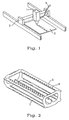
- Laser beam machining as shown in FIG.1 is best applied to formation of the grooves 8, where a quartz glass board 2 is placed on a working table for laser beam machining to cut grooves 8 for resting the waters, where the CO2 gas laser 1 is displaced by supporting arms 3 on rails.
- Ar assist gas 4 is blown into a groove 8 under cutting so as not to have a fume remain in the groove 8.
- the output power of laser beam for cutting is so adjusted as to obtain a smooth surface.
- the cutting of a dimensional precision of ⁇ 0.05 mm is executable, if position control in the cutting process is made by the unit of 1 ⁇ m.
- the color-changed portion is etched off by dipping in a diluted hydrofluoric acid. No crack occurs and the surface is smoothed, by adopting laser beam machining.
- Boards as molded by extrusion have a thickness variation of ⁇ at most about 0.3 mm and this variation does not adversely affect the uniformity of processing in laser beam machining. Boards as molded by extrusion are therefore preferably used in the present invention.
- the coverage of laser beam machining on the surface in the neighborhood of a wafer resting position is enough if it is conducted throughout the surface portion within 2 cm of the contact point with the silicon wafer inserted. With no laser beam machining beyond the surface portion, contamination of silicon wafers does not occur, even though diamond processing is applied there.
- High purity quartz crystal powders 12 are supplied in an electric furnace 9 as shown in FIGS. 3 and 4, molten by heating. The molten quartz is then extruded through the nozzle 10 to produce a quartz glass rod 11 or a quartz glass board 2.
- Each of the thus produced quartz glass boards 2 is set in a laser beam machine as shown in FIG.1, grooves for resting silicon wafers 8 are cut and then the machined quartz glass boards 2 and a supporting member 7 constructed from the quartz glass rods 11 are electrically welded with one another to complete a silicon wafer boat as shown in FIG.2.
- the method as described above relates to an example of the horizontal furnace boats, and a vertical furnace boat is also fabricatable forming grooves or teeth 8 for resting wafers by means of a similar method to that as mentioned above.
- Quartz crystal powders of raw material were treated by floatation and electromagnetic separation, washed in hydrofluoric acid and nitric acid and further refined with a mixed gas of chlorine and hydrogen chloride at 1100 °C.
- quartz crystal powders with such an impurity level as a concentration of Fe less than 0.05 ppm, a concentration of Na less than 0.05 ppm, a concentration of Ka less than 0.05 ppm and a concentration of Ca less than 0.5 ppm were obtained.
- the thus treated quartz crystal powders were heated in a molybdenum crucible disposed in an electric furnace 9 at 2200 °C to be transformed to transparent quartz glass.
- the quartz glass was then molded with a extruder as shown in FIGS.3 and 4 into round rods 11 of 15 mm in diameter and boards 2 of 4 mm thick and 35 cm wide.
- Grooves for resting wafers 8 were cut in and along some of the boards by means of a method of laser beam machining as shown in FIG.1 to complete wafer resting members 5 and next the wafer resting members 5 were welded to assemble a silicon wafer boat.
- the thus produced silicon wafer boat was washed in a hydrofluoric acid of 4.5 % in concentration for 3 minutes to remove the adhered fume and surface contamination.
- the internal surface in each of the grooves for resting wafers 8 was smooth.
- the concentration of Fe was less than 0.05 ppm
- the concentration of Na was less than 0.05 ppm
- the concentration of Ka was less than 0.05 ppm
- the concentration of Ca was less than 0.5 ppm. It is seen from the data that the purity level of the raw material was kept unchanged in the jig. Oxidation treatment on wafers was carried out using the wafer boat and as a result all the wafers had uniform oxide films of good quality.
- Grooves for resting wafers 8 were cut in a conventional method for cutting by a diamond tool 15 as shown in FIG.5 to complete a wafer boat and the purity level in the surface region up to 30 ⁇ m in depth of a wafer boat was analyzed in a way like the example as above-mentioned.
- a wafer boat produced in a similar way to that of the comparative example 1 was repeatedly treated in hydrofluoric acid to have been cleaned, while monitoring the surface purity level by the analyses of the etching solution.
- the boat was unable to be used as that for automatic loading, because the width of the opening of each of grooves was increased by more than about 0.1 mm and what's more a disorder in the shapes of the grooves was resulted.
- a wafer boat was prepared in a similar way to that of the example except that one of the outmost ends of the grooves in a row is cut with a diamond cutter and wafers were loaded in the wafer boat to execute oxide-film formation treatment. The result were that the wafers positioned within 2 cm of the outmost groove were of poor quality due to an excessive thickness of the oxide film.
Landscapes
- Container, Conveyance, Adherence, Positioning, Of Wafer (AREA)
- Glass Melting And Manufacturing (AREA)
Claims (5)
- Verfahren zur Herstellung einer Haitevorrichtung aus Quarzglas für die Wärmebehandfung von Silizium-Wafem, umfassend ein Bauteil zur Auflage der Silizium-Wafer (5), das eine Quarzglasplatte (2) aufweist, in und entlang derer Lagerillen (8) für die Wafer ausgebildet sind, dadurch gekennzeichnet, dass die Lagerillen für die Wafer durch Laserstrahl- Bearbeitung gebildet sind.
- Verfahren zur Herstellung einer Haltevorrichtung aus Quarzglas nach Anspruch 1, dadurch gekennzeichnet, dass benachbarte Bereiche der jeweiligen Lagerillen für die Wafer bis zu einem Abstand von 2 cm vom Wafer-Berührungspunkt mit Laserstrahlen bearbeitet werden.
- Verfahren zur Herstellung einer Haltevorrichtung aus Quarzglas nach Anspruch 1, dadurch gekennzeichnet, dass der Oberflächenbereich aller Quarzglasteile, aus denen die Haltevorrichtung aus Quarzglas für die Wärmebehandlung von Silizium-Wafern besteht, bis zu einer Tiefe von mindestens 30 µm mit einem Reinheitsgrad gebildet wird, der jeweils im Mittel eine Eisenkonzentration von 0,4 Gew.-ppm oder weniger, eine Natriumkonzentration von 0,4 Gew.-ppm oder weniger, eine Kaliumkonzentration von 0,2 Gew.-ppm oder weniger und eine Kalziumkonzentration von 0,8 Gew.-ppm oder weniger aufweist, indem diese Teile aus einem Quarzglas-Ausgangsmaterial mit demselben Reinheitsgrad geformt werden.
- Verfahren zur Herstellung einer Haltevorrichtung aus Quarzglas nach Anspruch 1, dadurch gekennzeichnet, dass die Quarzglasplatte mit einem Stützelement (7) verschweißt und durch dieses gestützt ist.
- Verfahren zur Herstellung einer Haltevorrichtung aus Quarzglas nach Anspruch 4, dadurch gekennzeichnet, dass die Quarzglasplatte durch Strangformen von in einem Tiegel geschmolzenen Siliziumdioxid hergestellt ist, wobei das Ausgangsmaterial des Siliziumdioxids einen mittleren Reinheitsgrad wie folgt aufweist: Eisenkonzentration 0,4 Gew.-ppm oder weniger, Natriumkonzentration 0,4 Gew.-ppm oder weniger, Kaliumkonzentration 0,2 Gew.-ppm oder weniger und Kalziumkonzentration 0,8 Gew.-ppm oder weniger.
Applications Claiming Priority (7)
| Application Number | Priority Date | Filing Date | Title |
|---|---|---|---|
| JP22896794 | 1994-08-31 | ||
| JP228968/94 | 1994-08-31 | ||
| JP22896894 | 1994-08-31 | ||
| JP6228967A JP2840198B2 (ja) | 1994-08-31 | 1994-08-31 | 半導体素子熱処理用石英ガラス治具とその製造方法 |
| JP228967/94 | 1994-08-31 | ||
| JP22896894A JP2802234B2 (ja) | 1994-08-31 | 1994-08-31 | シリコンウエハ熱処理用組合せ治具とその製造方法 |
| PCT/EP1995/003418 WO1996007199A2 (en) | 1994-08-31 | 1995-08-31 | Quartz glass jig for the heat treatment of silicon wafers and method and device for producing same |
Publications (2)
| Publication Number | Publication Date |
|---|---|
| EP0725978A1 EP0725978A1 (de) | 1996-08-14 |
| EP0725978B1 true EP0725978B1 (de) | 2003-01-08 |
Family
ID=26528564
Family Applications (1)
| Application Number | Title | Priority Date | Filing Date |
|---|---|---|---|
| EP95931948A Expired - Lifetime EP0725978B1 (de) | 1994-08-31 | 1995-08-31 | Verfahren zur herstellung einer quarzglas-haltevorrichtung zur wärmebehandlung von silizium-wafern |
Country Status (3)
| Country | Link |
|---|---|
| EP (1) | EP0725978B1 (de) |
| DE (1) | DE69529333T2 (de) |
| WO (1) | WO1996007199A2 (de) |
Families Citing this family (3)
| Publication number | Priority date | Publication date | Assignee | Title |
|---|---|---|---|---|
| JP4453995B2 (ja) | 2000-12-05 | 2010-04-21 | 信越石英株式会社 | フッ素系樹脂被覆石英ガラス製キャリアボート |
| JP4348542B2 (ja) * | 2004-08-24 | 2009-10-21 | 信越半導体株式会社 | 石英治具及び半導体製造装置 |
| CN107627163A (zh) * | 2017-11-01 | 2018-01-26 | 东莞市奇声电子实业有限公司 | 一种玻璃屏幕固定装置 |
Family Cites Families (5)
| Publication number | Priority date | Publication date | Assignee | Title |
|---|---|---|---|---|
| US3640398A (en) * | 1970-03-30 | 1972-02-08 | Edward J Mellen Jr | Wafer boat |
| DE8021868U1 (de) * | 1980-08-16 | 1981-01-29 | Heraeus Quarzschmelze Gmbh, 6450 Hanau | Traegerhorde fuer halbleiterscheiben |
| US4738573A (en) * | 1987-01-08 | 1988-04-19 | Johnson Jr Christian F | Silicon wafer processing boat carrier slot plunge cutter |
| DE8814987U1 (de) * | 1988-12-02 | 1989-04-06 | Westdeutsche Quarzschmelze GmbH & Co. KG, 2054 Geesthacht | Quarzglasbehälter für thermische Behandlung von Halbleiterscheibchen |
| US5042655A (en) * | 1989-09-27 | 1991-08-27 | E. I. Du Pont De Nemours & Co. | Pellicle packaging and handling system |
-
1995
- 1995-08-31 DE DE69529333T patent/DE69529333T2/de not_active Expired - Fee Related
- 1995-08-31 EP EP95931948A patent/EP0725978B1/de not_active Expired - Lifetime
- 1995-08-31 WO PCT/EP1995/003418 patent/WO1996007199A2/en not_active Ceased
Also Published As
| Publication number | Publication date |
|---|---|
| DE69529333T2 (de) | 2004-01-15 |
| EP0725978A1 (de) | 1996-08-14 |
| WO1996007199A2 (en) | 1996-03-07 |
| DE69529333D1 (de) | 2003-02-13 |
| WO1996007199A3 (en) | 1996-05-02 |
Similar Documents
| Publication | Publication Date | Title |
|---|---|---|
| US7484958B2 (en) | Vertical boat for heat treatment and method for producing the same | |
| US4382838A (en) | Novel silicon crystals and process for their preparation | |
| KR101408552B1 (ko) | 박형 실리콘 로드의 제조를 위한 방법 및 장치 | |
| KR101356303B1 (ko) | 다결정 실리콘 웨이퍼 | |
| CN105229208A (zh) | β-Ga2O3系单晶的培育方法以及β-Ga2O3系单晶基板及其制造方法 | |
| EP0725978B1 (de) | Verfahren zur herstellung einer quarzglas-haltevorrichtung zur wärmebehandlung von silizium-wafern | |
| KR100748376B1 (ko) | 석영 도가니의 재생방법 | |
| EP2143833A1 (de) | Siliziumkristallmaterial und verfahren zur herstellung eines fz-siliziumeinkristalls damit | |
| KR0171661B1 (ko) | 반도체 소자 열처리용 석영글라스 지그 및 그 제조방법 | |
| KR100500657B1 (ko) | 실리콘 단결정 제조용 종결정 및 실리콘 단결정의 제조방법 | |
| KR101823229B1 (ko) | 실리콘 웨이퍼의 제조 방법 | |
| JP2009182180A (ja) | 半導体ウェハーの製造方法及び半導体ウェハー | |
| KR20120085338A (ko) | 다결정 실리콘 블록재의 제조 방법, 다결정 실리콘 웨이퍼의 제조 방법 및 다결정 실리콘 블록재 | |
| JP2002237465A (ja) | 固相シートの製造方法 | |
| CN102047384A (zh) | 处理半导体材料方法和经处理的半导体材料 | |
| US3962000A (en) | Barium aluminoborosilicate glass-ceramics for semiconductor doping | |
| JP2004161575A (ja) | 多結晶シリコンインゴット及び部材の製造方法 | |
| JPH07183240A (ja) | 半導体製造用治具の製造方法 | |
| JP2005059354A (ja) | 半導体ウエハをスライスするための単結晶塊の製造方法 | |
| KR100201705B1 (ko) | 경면 연마 웨이퍼 제조방법 | |
| JP2911023B2 (ja) | シリコンウエハ熱処理用石英ガラス治具およびその使用方法 | |
| CN114207780A (zh) | 激光标记的印刷方法及带激光标记的硅晶片的制造方法 | |
| JP2802234B2 (ja) | シリコンウエハ熱処理用組合せ治具とその製造方法 | |
| RU2164267C1 (ru) | Способ выращивания профилированных кристаллов тугоплавких соединений | |
| JP2025147366A (ja) | 銅板および接合体 |
Legal Events
| Date | Code | Title | Description |
|---|---|---|---|
| PUAI | Public reference made under article 153(3) epc to a published international application that has entered the european phase |
Free format text: ORIGINAL CODE: 0009012 |
|
| 17P | Request for examination filed |
Effective date: 19960503 |
|
| AK | Designated contracting states |
Kind code of ref document: A1 Designated state(s): DE FR GB |
|
| RBV | Designated contracting states (corrected) |
Designated state(s): DE FR GB |
|
| 17Q | First examination report despatched |
Effective date: 19991209 |
|
| RAP1 | Party data changed (applicant data changed or rights of an application transferred) |
Owner name: SHIN-ETSU QUARTZ PRODUCTS CO., LTD. Owner name: HERAEUS QUARZGLAS GMBH & CO. KG |
|
| RTI1 | Title (correction) |
Free format text: METHOD OF PRODUCING A QUARTZ GLASS JIG FOR THE HEAT TREATMENT OF SILICON WAFERS |
|
| GRAH | Despatch of communication of intention to grant a patent |
Free format text: ORIGINAL CODE: EPIDOS IGRA |
|
| GRAH | Despatch of communication of intention to grant a patent |
Free format text: ORIGINAL CODE: EPIDOS IGRA |
|
| GRAA | (expected) grant |
Free format text: ORIGINAL CODE: 0009210 |
|
| AK | Designated contracting states |
Kind code of ref document: B1 Designated state(s): DE FR GB |
|
| REG | Reference to a national code |
Ref country code: GB Ref legal event code: FG4D |
|
| REF | Corresponds to: |
Ref document number: 69529333 Country of ref document: DE Date of ref document: 20030213 Kind code of ref document: P |
|
| PGFP | Annual fee paid to national office [announced via postgrant information from national office to epo] |
Ref country code: GB Payment date: 20030728 Year of fee payment: 9 |
|
| PGFP | Annual fee paid to national office [announced via postgrant information from national office to epo] |
Ref country code: DE Payment date: 20030805 Year of fee payment: 9 |
|
| PGFP | Annual fee paid to national office [announced via postgrant information from national office to epo] |
Ref country code: FR Payment date: 20030813 Year of fee payment: 9 |
|
| ET | Fr: translation filed | ||
| PLBE | No opposition filed within time limit |
Free format text: ORIGINAL CODE: 0009261 |
|
| STAA | Information on the status of an ep patent application or granted ep patent |
Free format text: STATUS: NO OPPOSITION FILED WITHIN TIME LIMIT |
|
| 26N | No opposition filed |
Effective date: 20031009 |
|
| PG25 | Lapsed in a contracting state [announced via postgrant information from national office to epo] |
Ref country code: GB Free format text: LAPSE BECAUSE OF NON-PAYMENT OF DUE FEES Effective date: 20040831 |
|
| PG25 | Lapsed in a contracting state [announced via postgrant information from national office to epo] |
Ref country code: DE Free format text: LAPSE BECAUSE OF NON-PAYMENT OF DUE FEES Effective date: 20050301 |
|
| GBPC | Gb: european patent ceased through non-payment of renewal fee |
Effective date: 20040831 |
|
| PG25 | Lapsed in a contracting state [announced via postgrant information from national office to epo] |
Ref country code: FR Free format text: LAPSE BECAUSE OF NON-PAYMENT OF DUE FEES Effective date: 20050429 |
|
| REG | Reference to a national code |
Ref country code: FR Ref legal event code: ST |