EP0723332B1 - Motor apparatus capable of obtaining high efficiency and motor control method - Google Patents
Motor apparatus capable of obtaining high efficiency and motor control method Download PDFInfo
- Publication number
- EP0723332B1 EP0723332B1 EP95926017A EP95926017A EP0723332B1 EP 0723332 B1 EP0723332 B1 EP 0723332B1 EP 95926017 A EP95926017 A EP 95926017A EP 95926017 A EP95926017 A EP 95926017A EP 0723332 B1 EP0723332 B1 EP 0723332B1
- Authority
- EP
- European Patent Office
- Prior art keywords
- signal
- voltage
- level
- motor
- phase correction
- Prior art date
- Legal status (The legal status is an assumption and is not a legal conclusion. Google has not performed a legal analysis and makes no representation as to the accuracy of the status listed.)
- Expired - Lifetime
Links
Images


Classifications
-
- H—ELECTRICITY
- H02—GENERATION; CONVERSION OR DISTRIBUTION OF ELECTRIC POWER
- H02P—CONTROL OR REGULATION OF ELECTRIC MOTORS, ELECTRIC GENERATORS OR DYNAMO-ELECTRIC CONVERTERS; CONTROLLING TRANSFORMERS, REACTORS OR CHOKE COILS
- H02P6/00—Arrangements for controlling synchronous motors or other dynamo-electric motors using electronic commutation dependent on the rotor position; Electronic commutators therefor
- H02P6/08—Arrangements for controlling the speed or torque of a single motor
-
- H—ELECTRICITY
- H02—GENERATION; CONVERSION OR DISTRIBUTION OF ELECTRIC POWER
- H02P—CONTROL OR REGULATION OF ELECTRIC MOTORS, ELECTRIC GENERATORS OR DYNAMO-ELECTRIC CONVERTERS; CONTROLLING TRANSFORMERS, REACTORS OR CHOKE COILS
- H02P6/00—Arrangements for controlling synchronous motors or other dynamo-electric motors using electronic commutation dependent on the rotor position; Electronic commutators therefor
- H02P6/14—Electronic commutators
- H02P6/16—Circuit arrangements for detecting position
- H02P6/18—Circuit arrangements for detecting position without separate position detecting elements
- H02P6/187—Circuit arrangements for detecting position without separate position detecting elements using the star point voltage
-
- H—ELECTRICITY
- H02—GENERATION; CONVERSION OR DISTRIBUTION OF ELECTRIC POWER
- H02P—CONTROL OR REGULATION OF ELECTRIC MOTORS, ELECTRIC GENERATORS OR DYNAMO-ELECTRIC CONVERTERS; CONTROLLING TRANSFORMERS, REACTORS OR CHOKE COILS
- H02P6/00—Arrangements for controlling synchronous motors or other dynamo-electric motors using electronic commutation dependent on the rotor position; Electronic commutators therefor
- H02P6/08—Arrangements for controlling the speed or torque of a single motor
- H02P6/085—Arrangements for controlling the speed or torque of a single motor in a bridge configuration
-
- H—ELECTRICITY
- H02—GENERATION; CONVERSION OR DISTRIBUTION OF ELECTRIC POWER
- H02P—CONTROL OR REGULATION OF ELECTRIC MOTORS, ELECTRIC GENERATORS OR DYNAMO-ELECTRIC CONVERTERS; CONTROLLING TRANSFORMERS, REACTORS OR CHOKE COILS
- H02P6/00—Arrangements for controlling synchronous motors or other dynamo-electric motors using electronic commutation dependent on the rotor position; Electronic commutators therefor
- H02P6/14—Electronic commutators
- H02P6/16—Circuit arrangements for detecting position
- H02P6/17—Circuit arrangements for detecting position and for generating speed information
-
- H—ELECTRICITY
- H02—GENERATION; CONVERSION OR DISTRIBUTION OF ELECTRIC POWER
- H02P—CONTROL OR REGULATION OF ELECTRIC MOTORS, ELECTRIC GENERATORS OR DYNAMO-ELECTRIC CONVERTERS; CONTROLLING TRANSFORMERS, REACTORS OR CHOKE COILS
- H02P2209/00—Indexing scheme relating to controlling arrangements characterised by the waveform of the supplied voltage or current
- H02P2209/07—Trapezoidal waveform
Definitions
- the present invention relates to a motor system capable of high efficiency operation.
- Brushless DC motors have conventionally been researched and developed for their application to various fields, and also put into practical use, taking advantage of their capability that no secondary copper loss is involved so that enhancement in efficiency is theoretically possible.
- the motor current is controlled based on the fact that the generated torque is the sum of magnet torque (a torque proportional to the q-axis current, which is a current in a direction perpendicular to that of gap magnetic flux) and reluctance torque (a torque proportional to the product of d- and q-axis currents), in such a way that optimum values for the d- and q-axis currents are obtained through the steps of detecting the load status (torque) and sequentially performing arithmetic operations to calculate the optimum values of the d- and q-axis currents (see "High Efficiency Control of Brushless DC Motors for Energy Saving,” Morimoto et al., T.IEE Japan, Vol. 112-D, No. 3, '92, in particular, Equations (14) and (15)).
- the method (i) allows easy application to such fields as would demand high-speed torque response, for example, brushless DC motor drive systems used in machine tools, industrial robots, and the like, where a voltage-fed inverter is previously provided with an instantaneous current detector to implement a high-speed current control system so that there is no need of providing a special device for high efficiency. It is because the current response becomes generally equal to the torque response in brushless DC motors that the high-speed current control system is implemented. This allows a high-speed torque response to be realized.
- the brushless DC motor drive system in household electrical appliances such as air conditioners, washers, and cleaners is based on a simple control system in which the voltage waveform is controlled by only a voltage-fed inverter in response to a position signal derived from detecting the position of the rotor of the brushless DC motor. Therefore, the above (i) method, if applied, would make it necessary not only to newly provide an instantaneous current detector but also to enhance the control operation function, particularly when a buried-magnet DC motor is adopted. As a result, a high-performance microcomputer needs to be substituted for or be added to an existing microcomputer, which incurs a great increase in cost.
- the motor is enabled to attain high-efficiency operation as far as the operation is limited to around the rated point.
- the motor generally runs quite away from the rated point considerably longer than it does around the rated point. In the operation during the former period, the current value would not lower even if the voltage amplitude is reduced with a less load, so that a current more than necessary would be passed.
- the motor can be operated only at efficiencies lower than its best possible efficiency (peak efficiency at different load conditions) to a disadvantage.
- a buried-magnet DC motor with a d-axis inductance Ld of 65 mH and a q-axis inductance Lq of 15.0 mH and a counter-electromotive voltage coefficient Ke of 0.105 Vs/rad is driven at a rotation speed 90 rps., and if the phase of the motor counter-electromotive voltage and the phase of the inverter output voltage are set to 50° and 80°, respectively, then it can be understood from Fig.
- Fig. 3 is a block diagram schematically showing the arrangement of a conventional brushless DC motor system
- Fig. 4 is a block diagram showing the main part of the control circuit in Fig. 3.
- the conventional brushless DC motor system is so arranged that an AC voltage 91 is converted into a DC voltage by a converter 92a of a voltage-fed inverter 92 and thereafter converted into an AC voltage by an inverter main part 92b and, as such, supplied to a brushless DC motor 93, where the magnetic-pole position of the rotor of the brushless DC motor 93 is detected by a position sensor circuit 94 and a switching command is generated by a control circuit 96 in response to a magnetic-pole position detection signal and then fed to the voltage-fed inverter 92.
- the control circuit 96 comprises an amplitude command output section 96a for receiving inputs of, for example, an actual rotation speed and a rotation speed command, which are obtained based on the time interval of magnetic-pole position detection signals outputted by the position sensor circuit 94, and a phase table 96b for outputting a phase command corresponding to the actual rotation speed by taking the actual rotation speed as a read address, whereby an amplitude command and a phase command are fed to an unshown PWM circuit so that a switching command is generated.
- an amplitude command output section 96a for receiving inputs of, for example, an actual rotation speed and a rotation speed command, which are obtained based on the time interval of magnetic-pole position detection signals outputted by the position sensor circuit 94
- a phase table 96b for outputting a phase command corresponding to the actual rotation speed by taking the actual rotation speed as a read address, whereby an amplitude command and a phase command are fed to an unshown PWM circuit so that a switching command is generated.
- a switching command is generated by feeding the amplitude command V* calculated from the difference between rotation speed command Y* and actual rotation speed Y as well as a phase command read from the phase table 96b to the PWM circuit, whereby the actual rotation speed Y can be approached and equalized to the rotation speed command Y*.
- Fig. 5 shows an equivalent circuit of one phase portion of the brushless DC motor.
- this equivalent circuit has a motor winding resistance R, a reactance Xq on the q-axis, and an induced voltage (more precisely, a voltage resulting from adding the product of a difference between q-axis reactance Xq and d-axis reactance Xd and a d-axis component Id of motor current to the counter-electromotive voltage E) connected in series with the inverter fundamental-wave voltage V in this order.
- j in Fig. 5 represents an imaginary number.
- the rotation speed of the brushless DC motor is controlled by adjusting the voltage amplitude of the voltage-fed inverter (PWM duty factor)
- the phase is fixed so that the voltage amplitude command will not be saturated at the time of acceleration in order to stably operate the speed control system.
- PWM duty factor the voltage amplitude of the voltage-fed inverter
- EP-A1-0 589 630 discloses a circuit and method for automatically adjusting a commutation delay from events indicating a position of a polyphase dc motor.
- the circuit includes a driver to supply drive current to selected stator coils of said motor.
- a sequencer is connected to control the driver to apply drive current to selected motor coils to rotate the motor.
- Motor position detecting circuitry is connected to detect the events indicating the position of the motor.
- a commutation delay circuit is connected to increment the sequencer in response to the detection of the events indicating the position of the motor detected by the motor position detecting circuitry.
- a circuit for adjusting the delay of said commutation delay circuit between each event and each sequencer commutation provides optimum motor commutation for maximum power efficiency.
- drive current is supplied to selected stator coils of said motor in predetermined commutated sequences to rotate the motor.
- Events are detected indicating the position of the motor, and the delay between each position indicating event and each commutation sequence is automatically adjusted to provide optimum motor commutation for maximum power efficiency.
- US-A-4 641066 discloses a control apparatus which detects a suitable starting point during rotational oscillation of a rotor at the start of a brushless motor by combining the polarity of a counter electromotive force generated in an armature coil of an armature winding of the brushless motor for a nonexcited phase due to the rotational oscillation of the rotor (when armature coils for particular phases are excited at the start of the brushless motor) with the pulse edge of an excitation switchover signal obtained from the potential of a neutral point of the armature winding having the armature coils connected in star-connection and that of a neutral point of a detecting resistance circuit having resistors connected in star-connection.
- Each of the resistors of the resistance circuit is arranged in parallel with a corresponding one of the armature coils of the armature winding.
- the present invention has been achieved in view of the aforementioned problems.
- An object of the present invention is to provide a motor system (DC or AC motor system) which can be operated at peak efficiency while the motor can be prevented from stepping out.
- the present invention provides a motor system according to independent claims 1 and 2. Preferred embodiments of the invention are indicated in the dependent claims.
- the present invention provides a motor system including a rotor, a stator having armature coils, an inverter for switching a voltage pattern to be applied to the armature coils, the motor system being characterized by further comprising a control means for controlling an output of the inverter so that a specified efficiency (desirably, peak efficiency) is obtained, based on a neutral-point voltage of the armature coils.
- a specified efficiency desirably, peak efficiency
- the control means operates the motor at a desired efficiency by performing phase control or voltage control of an output of the inverter based on a neutral-point voltage of the armature coils.
- the motor can be operated at an arbitrary efficiency by controlling the output of the inverter based on the neutral-point voltage with the use of the characteristic of the neutral-point voltage of the armature coils with respect to the motor efficiency. Also, when the motor steps out with the level of the neutral-point voltage of the armature coils less than a certain value, the motor can be prevented from stepping out by controlling the output of the inverter so that the level of the neutral-point voltage will not become less than a certain value.
- the armature coils are connected in a three-phase star configuration and comprise a resistor circuit connected in three-phase star configuration in parallel to the armature coils and a rotor-position sensor means for detecting a relative rotor position between the rotor and the stator, and thereby outputting a position signal.
- the control means comprises a level decision means for deciding a relationship how a level of a voltage difference signal representing a voltage difference between the neutral point of the armature coils and a neutral point of the resistor circuit is related to a target value (desirably, a target value at which a peak efficiency is obtained), and a phase correction means for adjusting a time interval from the position signal to a switching of the voltage pattern so that the level of the voltage difference signal becomes the target value, based on a decision result of the level decision means.
- the inverter switches over the voltage pattern to be applied to the armature coils, based on a signal representing the phase-corrected voltage pattern derived from the phase correction means.
- the motor can be operated at an arbitrary efficiency by setting the target value with which the level of the voltage difference signal is decided, to a level at which a desired efficiency is obtained. Also, the motor can be prevented from stepping out, based on the ground that the phase of voltage pattern is not adjusted to the step-out area pattern on the phase lag side of the peak efficiency point when the motor is operated at a desired efficiency with the voltage pattern gradually adjusted from leading to lagging phase.
- the control means comprises a level decision means for deciding a relationship how a level of an integral signal derived from integrating a voltage difference signal representing a voltage difference between the neutral point of the armature coils and a neutral point of the resistor circuit is related to a target value (desirably, a target value at which a peak efficiency is obtained), and a phase correction means for adjusting a time interval from the position signal to a switching of the voltage pattern so that the level of the integral signal becomes the target value, based on a decision result of the level decision means.
- the inverter switches over the voltage pattern to be applied to the armature coils based on a signal representing the phase-corrected voltage pattern derived from the phase correction means.
- the motor can be operated at an arbitrary efficiency by setting the target value with which the level of the integral signal is decided, to a level at which a desired efficiency is obtained. Also, the motor can be operated at a specified efficiency more easily than it is by deciding the level of a voltage difference signal, if the level of the integral signal with the desired efficiency is generally constant even with varying running frequency, on the ground that the integral signal is obtained by integrating a voltage difference signal. Further, the motor can be prevented from stepping out, based on the ground that the phase of voltage pattern is not adjusted to the step-out area pattern on the phase lag side of the peak efficiency point when the motor is operated at a desired efficiency with the voltage pattern gradually adjusted from leading to lagging phase.
- the armature coils are connected in a three-phase star configuration and comprise a resistor circuit connected in a three-phase star configuration in parallel to the armature coils
- the control means comprises a level decision means for deciding a relationship how a level of a voltage difference signal representing a voltage difference between the neutral point of the armature coils and a neutral point of the resistor circuit is related to a target value (desirably, a target value at which a peak efficiency is obtained), and a voltage correction means for correcting an output voltage of the inverter so that the level of the voltage difference signal becomes the target value, based on a decision result of the level decision means.
- the motor can be operated at an arbitrary efficiency by setting the target value with which the level of the voltage difference signal is decided, to a level at which a desired efficiency is obtained. Also, the motor can be prevented from stepping out, based on the ground that the output voltage is not adjusted to the step-out area on a side where the output voltage is higher than the peak efficiency point when the motor is operated at a desired efficiency by adjusting the output voltage of the inverter so that it becomes gradually higher from a voltage lower than the output voltage at the peak efficiency point.
- control means comprises a level decision means for deciding a relationship how a level of an integral signal derived from integrating a voltage difference signal representing a voltage difference between the neutral point of the armature coils and a neutral point of the resistor circuit is related to a target value (desirably, a target value at which a peak efficiency is obtained), and a voltage correction means for correcting an output voltage of the inverter so that the level of the integral signal becomes the target value, based on a decision result of the level decision means.
- a target value desirably, a target value at which a peak efficiency is obtained
- the motor can be operated at an arbitrary efficiency by setting the target value with which the level of the integral signal is decided, to a level at which a desired efficiency is obtained. Also, since the integral signal is obtained by integrating a voltage difference signal, the motor can be operated at a specified efficiency more easily than it is by deciding the level of the voltage difference signal, when the level of the integral signal at the desired efficiency becomes generally constant even with varying running frequency.
- the motor can be prevented from stepping out, based on the ground that the output voltage is not adjusted to the step-out area on a side where the output voltage is higher than the peak efficiency point when the motor is operated at a desired efficiency by adjusting the output voltage of the inverter so that it becomes gradually higher from a voltage lower than the output voltage at the peak efficiency point.
- Fig. 7 shows a construction of a brushless DC motor system of a fourth embodiment of the present invention, in which reference numeral 1 denotes a stator which has star-connected armature coils 1a, 1b and 1c and rotates a rotor 10 having a plurality of permanent magnets by a rotating magnetic field, reference numeral 2 denotes a resistor circuit having star-connected resistors 2a, 2b and 2c connected in parallel with the armature coils 1a, 1b and 1c, reference numeral 3 denotes a rotational-position sensor which serves as rotational-position sensor means that detects a voltage difference signal V MN representing a voltage difference between a voltage V M at a neutral point of the resistor circuit 2 and a voltage V N at a neutral point of the armature coils 1a, 1b and 1c, detects a relative position of the rotor 10 based on the voltage difference signal V MN , and outputs a position signal representing the relative position of the rotor 10, reference nume
- the rotational-position sensor 3 includes an amplifier IC1 where the voltage V M at the neutral point of the resistor circuit 2 is inputted to an inverted input terminal thereof, a ground GND is connected to a non-inverted input terminal thereof via a resistor R 1 , and a resistor R 2 and a capacitor C 1 are connected in parallel with each other between an output terminal thereof and the inverted input terminal; an amplifier IC2 where an inverted input terminal thereof is connected to the output terminal of the amplifier IC1 via a resistor R 3 , a ground GND is connected to a non-inverted input terminal thereof via a resistor R 4 , and a resistor R 5 is connected between an output terminal thereof and the inverted input terminal; and an amplifier IC3 where an inverted input terminal thereof is connected to the output terminal of the amplifier IC2, a ground GND is connected to a non-inverted input terminal thereof via a resistor R 6 , and a resistor R 7 is connected between an output terminal thereof and the non-inverted input terminal.
- the amplifier IC1, resistor R 1 , resistor R 2 , and capacitor C 1 constitute concurrently a differential amplifier 21 and an integrator 22 which serves as integration means.
- the amplifier IC2 and the resistors R 3 , R 4 and R 5 constitute an inverting amplifier 23, while the amplifier IC3 and the resistors R 6 and R 7 constitute a zero-crossing comparator 24.
- the neutral point of the armature coils 1a, 1b and 1c is connected to the non-inverted input terminal of the amplifier IC1 via the ground GND and the resistor R 1 .
- the differential amplifier 21 detects the voltage difference signal V MN representing the voltage difference between the voltage V M at the neutral point of the resistor circuit 2 and the voltage V N at the neutral point of the armature coils 1a, 1b and 1c, integrates the voltage difference signal V MN , and outputs an integral signal ⁇ V MN dt.
- the above-mentioned brushless DC motor system includes a level detector 6 which receives the integral signal ⁇ V MN dt from the integrator 22 of the rotational-position sensor 3 and outputs a level detection signal to the microcomputer 4.
- the integral signal ⁇ V MN dt from the integrator 22 of the rotational-position sensor 3 is inputted to an inverted input terminal of an amplifier IC4, a non-inverted input terminal of the amplifier IC4 is connected to the ground GND via a resistor R 6 , and a resistor R 7 is connected between an output terminal and the non-inverted input terminal of the amplifier IC4.
- the amplifier IC4 and the resistors R 6 and R 7 constitute a hysteresis comparator having a hysteresis characteristic.
- the brushless DC motor is driven in accordance with the position signal, and as shown in Fig. 27, when the integral signal ⁇ V MN dt (shown in Fig. 27 (A)) inputted to the inverted input terminal of the amplifier IC4 of the level detector 6 exceeds a reference value E1, the output terminal of the amplifier IC4 comes to have L-level. When the integral signal ⁇ V MN dt becomes smaller than a reference value E2, the output terminal of the amplifier IC4 comes to have H-level. That is, the level detection signal (shown in Fig.
- the level detector 6 of the level detector 6 is a signal having a cycle identical to that of the position signal (shown in Fig. 10 (B)) and a phase different from that of the position signal.
- the level detection signal has a frequency lower than that of the position signal and a different duty ratio. In other words, whether or not the integral signal ⁇ V MN dt has a level not smaller than a specified level can be detected depending on whether or not the level detection signal is continuous in a specified cycle.
- the inverter section 20 includes three transistors 20a, 20b and 20c connected to a positive side of a DC power supply 9 and three transistors 20d, 20e and 20f connected to a negative side of the DC power supply 9.
- An emitter of the transistor 20a and a collector of the transistor 20d are connected to each other, an emitter of the transistor 20b and a collector of the transistor 20e are connected to each other, and an emitter of the transistor 20c and a collector of the transistor 20f are connected to each other.
- connection point of the transistors 20a and 20d is connected with the armature coil 1a of the U-phase
- connection point of the transistors 20b and 20e is connected with the armature coil 1b of the V-phase
- connection point of the transistors 20c and 20f is connected with the armature coil 1c of the W-phase.
- diodes are connected in an inverse-parallel connection form between the collectors and the emitters of the transistors 20a through 20f.
- the microcomputer 4 includes a phase correction timer T1 to which the position signal from the rotational-position sensor 3 shown in Fig. 24 is inputted via an external interrupt terminal; a cycle measuring timer T2 which receives the position signal and measures a cycle of the voltage pattern of the armature coils 1a, 1b and 1c; a cycle calculator 41 which receives a measured timer value from the cycle measuring timer T2, calculates a cycle of the voltage pattern of the armature coils 1a, 1b and 1c from the timer value, and outputs a cycle signal representing the cycle; and a timer value calculator 42 which receives the cycle signal from the cycle calculator 41, calculates a timer value corresponding to a phase correction angle based on the cycle, and outputs a timer value set signal to the phase correction timer T1.
- a phase correction timer T1 to which the position signal from the rotational-position sensor 3 shown in Fig. 24 is inputted via an external interrupt terminal
- a cycle measuring timer T2 which receives the position
- the microcomputer 4 further includes an inverter mode selector 43 which receives an interrupt signal IRQ from the phase correction timer T1 and outputs a voltage pattern signal; a speed calculator 44 which receives the cycle signal from the cycle calculator 41, calculates a rotation speed, and outputs a current-time speed signal; a speed controller 45 which receives the current-time speed signal from the speed calculator 44 and an external speed command signal, and outputs a voltage command signal; a level decision section 51 which receives the position signal from the rotational-position sensor 3 and the level detection signal from the level detector 6, and outputs a phase correction command signal to the timer value calculator 42; and a PWM (Pulse Width Modulation) modulator 52 which receives the voltage pattern signal from the inverter mode selector 43 and the voltage command signal from the speed controller 45, and outputs a switching signal.
- the phase correction timer T1, the cycle measuring time T2, the cycle calculator 41, and the timer value calculator 42 constitute phase correction means.
- the inverting amplifier 23 amplifies the integral signal ⁇ V MN dt inputted to the inverted input terminal of the amplifier IC2 to a specified amplitude, while the zero-crossing comparator 24 detects a zero-crossing point of the amplified integral signal ⁇ V MN dt and outputs a position signal (shown in Fig. 11 (F)).
- the position signal from the rotational-position sensor 3 is inputted through the external interrupt terminal of the microcomputer 4 to the cycle measuring timer T2.
- the cycle measuring timer T2 measures a period from a leading edge to a trailing edge of the position signal and a period from a trailing edge to a leading edge of the position signal, and outputs a timer value representing each measured period.
- the cycle calculator 41 Upon receiving a signal representing the timer value from the cycle measuring timer T2, the cycle calculator 41 obtains a cycle of the voltage pattern of the armature coils 1a, 1b and 1c.
- the period from the leading edge to the trailing edge of the position signal and the period from the trailing edge to the leading edge of the position signal are repeated every 60 degrees, so that by multiplying the timer value for each measured period by six, a timer value per cycle of the voltage pattern is obtained.
- the timer value calculator 42 outputs the timer value set signal.
- the phase correction timer T1 counts a time from the position signal to the switching of the voltage pattern. That is, when completing the counting, the phase correction timer T1 outputs the interrupt signal IRQ to the inverter mode selector 43, and the inverter mode selector 43 outputs phase-corrected voltage pattern signals (shown in Fig. 11 (I) through (N)) to the PWM modulator 52. Then, the PWM modulator 52 outputs the switching signal to the base drive circuit 5 shown in Fig.
- step S101 when the interrupt handling process 1 starts, it is decided whether or not a preceding-time level detection signal is at H-level at step S101.
- the program flow proceeds to step S121 to decide whether or not a current-time level detection signal is at L-level.
- step S122 When it is decided that the current-time level detection signal is at L-level at step S121, the program flow proceeds to step S122 to increment a counter CNT1 by one.
- the program flow proceeds to step S102.
- step S123 it is decided whether or not the current-time level detection signal is at H-level.
- step S124 the program flow proceeds to step S124 to increment the counter CNT1 by one.
- step S102 the program flow proceeds to step S102.
- a counter CNT2 is incremented by one at step S102, and the program flow proceeds to step S103. Then, it is decided whether or not the value of the counter CNT2 is 5 at step S103. When it is decided that the value of the counter CNT2 is 5, the program flow proceeds to step S125. When it is decided that the value of the counter CNT2 is not 5, the program flow proceeds to step S104 shown in Fig. 30. Then, it is decided whether or not the value of the counter CNT1 is 5 at step S125. When it is decided that the counter CNT1 indicates 5, the program flow proceeds to step S126 to increment by one degree a preceding-time phase correction angle command (to the lag correction side), and the program flow proceeds to step S129.
- step S127 decides whether or not the counter CNT1 is 0.
- step S128 decrement by one degree the preceding-time phase correction angle command (to the lead correction side), and the program flow proceeds to step S129.
- step S129 the program flow proceeds to step S129.
- step S130 the program flow proceeds to step S130 to clear the counter CNT2, and proceeds to step S104. It is to be noted that an initial value is set to the phase correction angle command and the counters CNT1 and CNT2 are cleared before the initial interrupt handling process 1 starts.
- step S104 shown in Fig. 13 it is decided whether or not the phase correction timer T1 (referred to as a timer T1 in Fig. 30) is counting.
- the program flow proceeds to step S131 to stop the timer T1. That is, when the timer T1 is counting, the timer T1 is stopped to be ready for the next start.
- a voltage pattern is outputted at step S132, and the program flow proceeds to step S105.
- the program flow proceeds to step S105.
- a correction angle (phase correction angle based on the phase correction command signal from the level decision section 51) is not smaller than 60 degrees.
- the program flow proceeds to step S141 to decide whether or not the correction angle is not smaller than 120 degrees.
- the program flow proceeds to step S142 to establish a phase correction E (referred to as a correction E in Fig. 13), and proceeds to step S143.
- it is decided whether or not the preceding phase correction is a phase correction C (referred to as a correction C in Fig. 13) or a phase correction D (referred to as a correction D in Fig. 13) at step S143.
- step S144 When it is decided that the preceding phase correction is the phase correction C or the phase correction D, the program flow proceeds to step S144 to issue a correction switching request, and thereafter proceeds to step S106. Otherwise, when it is decided that the preceding phase correction is neither the phase correction C nor the phase correction D at step S143, the program flow proceeds to step S106.
- step S145 to establish a phase correction D
- step S146 it is decided whether or not the preceding phase correction is the phase correction C or the phase correction E at step S146.
- the program flow proceeds to step S147 to issue a correction switching request, and thereafter proceeds to step S106. Otherwise, when it is decided that the preceding phase correction is neither the phase correction C nor the phase correction E at step S146, the program flow proceeds to step S106.
- step S151 When it is decided that the correction angle is smaller than 60 degrees at step S105, the program flow proceeds to step S151 to establish a phase correction C, and proceeds to step S152. Then, it is decided whether or not the preceding phase correction is the phase correction D or the phase correction E at step S152. When it is decided that the preceding phase correction is the phase correction D or the phase correction E, the program flow proceeds to step S153 to issue a correction switching request, and thereafter proceeds to step S106. Otherwise, when it is decided that the preceding phase correction is neither the phase correction D nor the phase correction E at step S152, the program flow proceeds to step S106.
- a timer value TISOU is calculated every time of phase corrections C, D and E. That is, in the phase correction C, a timer value corresponding to the phase correction angle is set to the timer value TISOU. In the phase correction D, a timer value corresponding to a phase angle obtained by subtracting 60 degrees from the phase correction angle is set to the timer value TISOU. In the phase correction E, a timer value corresponding to a phase angle obtained by subtracting 120 degrees from the phase correction angle is set to the timer value TISOU. Then, the program flow proceeds to step S107 to increment the inverter mode by one step.
- step S108 shown in Fig. 14, and it is decided whether or not the correction switching request is there.
- the program flow proceeds to step S161 to decide whether the correction mode is switched from the phase correction C (referred to as a correction C in Fig. 14) to the phase correction D (referred to as a correction D in Fig. 14) or from the phase correction D to the phase correction E (referred to as a correction E in Fig. 13).
- step S162 When it is decided that the correction mode is switched from the phase correction C to the phase correction D or from the phase correction D to the phase correction E, the program flow proceeds to step S162 to cancel the correction switching request, the inverter mode is put back by one step at step S162-1, and the program flow proceeds to step S109.
- step S163 the program flow proceeds to step S164 to set the timer value TISOU calculated at step S106 to the timer T1, and thereafter the timer T1 is started at step S165. Then, the program flow proceeds to step S166 to cancel the correction switching request, and proceeds to step S109.
- step S108 When it is decided that there is no correction switching request at step S108, the program flow proceeds to step S168 to set the timer value TISOU calculated at step S106 to the timer T1, the timer T1 is started at step S169, and the program flow proceeds to step S109.
- step S109 the cycle measuring timer T2 is stopped and a timer value of the cycle measuring timer T2 is read at step S109, and the program flow proceeds to step S110.
- the cycle measuring timer T2 is set and started at step S110 to start the next cycle measurement.
- a cycle is calculated from the value of the cycle measuring timer T2 in the cycle calculator 41 at step S111, and from the calculation result, the rotation speed of the motor is calculated in the speed calculator 44.
- the speed controller 45 executes speed control in response to an external speed command signal to output a voltage command signal at step S112.
- phase correction C effects a phase correction of 0 degree to 60 degrees
- phase correction D effects a phase correction of 60 degrees to 120 degrees
- phase correction E effects a phase correction of 120 degrees to 180 degrees.
- Figs. 11 (A) through (O) show signals at individual portions of the present brushless DC motor system in the process of phase correction D for effecting a phase correction of 80 degrees.
- the timer T1 starts sequentially for each of the position signal numbers (shown in Fig. 11 (G)).
- the phase correction angle is set to 80 degrees with respect to a reference point established, for example, at a point where the position signal number changes from 2 to 3, the position signal number is delayed by one from the reference point, so that the timer T1 starts at a point where the position signal number changes from 3 to 4, and that the inverter mode (shown in Fig. 11 (P)) is incremented by one step to [0] with a delay of 80 degrees from the reference point.
- the interrupt handling process 1 it is decided whether or not the change in level of the level detection signal from H-level to L-level and from L-level to H-level continuously occurs every time the interrupt handling process 1 is executed five times.
- the phase of the voltage pattern is delayed one degree by one degree toward the lag correction side.
- the phase of the voltage pattern is advanced one degree by one degree toward the lead correction side.
- the aforementioned integral signal ⁇ V MN dt comes to have a level set by the reference values E1 and E2 of the level detector 6.
- the phase correction is effected by setting the reference values E1 and E2 at the amplitude value of the integral signal ⁇ V MN dt at the peak motor efficiency point so that the level of the integral signal ⁇ V MN dt becomes a target value at the peak motor efficiency point.
- the motor is operated at the peak motor efficiency point.
- the phase correction angle is not adjusted, and the motor is operated stably at the peak motor efficiency point.
- the motor can be operated at the peak motor efficiency point regardless of the magnitude of the load and the pitch of the running frequency. Furthermore, by adjusting the phase of the voltage pattern gradually from the lead correction side to the lag correction side so as to achieve the peak motor efficiency point, the phase of the voltage pattern is prevented from being adjusted to a step-out region existing on the lag correction side of the peak efficiency point. Therefore the step out is prevented.
- Fig. 16 shows a construction of the brushless DC motor system used for the experiment.
- the brushless DC motor system has the same construction as that of the brushless DC motor system of the first embodiment except for a rotational-position sensor 30 and a microcomputer 14, and therefore no description is provided therefor.
- Fig. 17 shows a construction of the microcomputer 14 which has a construction formed by excluding the level decision section 51 from the microcomputer 4 shown in Fig. 9. Therefore, the same components are denoted by the same reference numerals, and no description is provided therefor. It is to be noted that an interrupt handling process for correcting the phase of the microcomputer 14 is executed in the same manner as that of the flow charts of Figs. 12, 13, 14 and 15 except for the steps S101, 102, 103 and 120 through 130.
- the rotational-position sensor 30 includes: a differential amplifier 31 in which the voltage V M at the neutral point of the resistor circuit 2 is inputted to a non-inverted input terminal of an amplifier IC11, a ground GND is connected to an inverted input terminal of the amplifier IC11 via a resistor R 11 , and a resistor R 12 is connected between an output terminal and an inverted input terminal of the amplifier IC11; an integrator 32 comprised of a resistor R 13 of which one end is connected to the output terminal of the differential amplifier 31 and a capacitor C 11 connected between the other end of the resistor R 13 and the ground GND; and a zero-crossing comparator 33 comprised of an amplifier IC12 which has its non-inverted input terminal connected to the other end of the resistor R 13 of the integrator 32 and has its inverted input terminal connected to the ground GND.
- the neutral point of the armature coils 1a, 1b and 1c is connected to the inverted input terminal of the differential amplifier 31 via the ground GND. Therefore, the differential amplifier 31 detects the voltage difference signal V MN representing the voltage difference between the voltage V M at the neutral point of the resistor circuit 2 and the voltage V N at the neutral point of the armature coils 1a, 1b and 1c.
- the differential amplifier 31 of the rotational-position sensor 30 detects the voltage difference signal V MN representing the voltage difference between the voltage V M at the neutral point of the resistor circuit 2 and the voltage V N at the neutral point of the armature coils 1a, 1b and 1c. Then, the integrator 32 integrates the voltage difference signals V MN so as to output an integral signal ⁇ V MN dt, and inputs the integral signal ⁇ V MN dt to the non-inverted input terminal of the zero-crossing comparator 33. Then, the zero-crossing comparator 33 compares the integral signal ⁇ V MN dt with a reference voltage at the ground GND, and outputs a position signal.
- the position signal from the zero-crossing comparator 33 is inputted through an external interrupt terminal of the microcomputer 14 to the cycle measuring timer T2.
- the cycle measuring timer T2 measures a period from a leading edge to a trailing edge of the position signal and a period from a trailing edge to a leading edge of the position signal, and outputs a timer value representing each measured period.
- the cycle calculator 41 obtains a cycle of the voltage pattern of the armature coils 1a, 1b and 1c.
- the timer value calculator 42 outputs the timer value set signal.
- the phase correction timer T1 counts a time from the position signal to the switching of the voltage pattern. That is, when completing the counting, the phase correction timer T1 outputs the interrupt signal IRQ to the inverter mode selector 43, and the inverter mode selector 43 outputs phase-corrected voltage pattern signals to the PWM modulator 52.
- the PWM modulator 52 outputs a switching signal to the base drive circuit 5 shown in Fig. 16, and the base drive circuit 5 outputs a commutation control signal to the inverter section 20, so that the transistors 20a through 20f of the inverter section 20 are tuned on and off, respectively.
- a characteristic curve of the motor efficiency relative to the phase correction angle exhibits a curve as shown in Fig. 18 where the curve shifts to the lead correction side of the phase correction angle according as the load increases, and the curve shifts to the lag correction side of the phase correction angle according as the load decreases. Then, the peak efficiency point takes place at a phase correction angle of ⁇ 1 when the load is great, and the peak efficiency point takes place at a phase correction angle of ⁇ 2 when the load is small.
- the characteristic of the voltage difference signal V MN relative to the phase correction angle is represented by an approximately straight line, as shown in Fig. 19, which indicates that the level of the voltage difference signal V MN gradually reduces according as the phase correction angle advances from the lead correction side to the lag correction side.
- the line shifts to the lead correction side of the phase correction angle according as the load increases, and the line shifts approximately parallel from the lead correction side to the lag correction side of the phase correction angle according as the load decreases.
- the axis of abscissas of Fig. 19 represents the phase correction angle
- the axis of ordinates represents a level ranging from the peak point to the zero point of the voltage difference signal V MN .
- the level of the voltage difference signal V MN is V0 at a phase correction angle of ⁇ 1 when the load is great, and the level of the voltage difference signal V MN is V0 at a phase correction angle of ⁇ 2 when the load is small. That is, it can be understood that the voltage difference signal V MN at the peak efficiency point is approximately constant regardless of the variation of the load.
- the motor steps out at a phase correction angle of ⁇ 11 located further on the lag correction side than the phase correction angle of ⁇ 1 is.
- the level of the voltage difference signal V MN then is V20.
- the motor steps out at a phase correction angle of ⁇ 12 located further on the lag correction side than the phase correction angle of ⁇ 2 is.
- the level of the voltage difference signal V MN then is V20.
- the characteristic of the integral signal ⁇ V MN dt relative to the phase correction angle exhibits an approximately straight line which indicates, as shown in Fig. 20, that the level of the integral signal ⁇ V MN dt gradually reduces according as the phase correction angle advances from the lead correction side to the lag correction side.
- the line shifts to the lead correction side of the phase correction angle according as the load increases, and the line shifts approximately parallel from the lead correction side to the lag correction side of the phase correction angle according as the load decreases.
- the axis of abscissas of Fig. 20 represents the phase correction angle
- the axis of ordinates represents a level ranging from the peak point to the zero point of the integral signal ⁇ V MN dt.
- the level of the integral signal ⁇ V MN dt is V1 at a phase correction angle of ⁇ 1 when the load is great, and the level of the integral signal ⁇ V MN dt is V1 at a phase correction angle of ⁇ 2 when the load is small. That is, it can be understood that the integral signal ⁇ V MN dt at the peak efficiency point is approximately constant regardless of the variation of the load.
- the motor steps out at a phase correction angle of ⁇ 11 located further on the lag correction side than the phase correction angle of ⁇ 1 is, and the level of the integral signal ⁇ V MN dt then is V21.
- the motor steps out at a phase correction angle of ⁇ 12 located further on the lag correction side than the phase correction angle of ⁇ 2, and the level of the integral signal ⁇ V MN dt then is V21.
- the characteristic of the voltage difference signal V MN relative to the phase correction angle exhibits an approximately straight line which indicates that, as shown in Fig. 22, the level of the voltage difference signal V MN gradually lowers as the phase correction angle advances from the lead correction side to the lag correction side.
- the line shifts to the lag correction side of the phase correction angle according as the running frequency increases, and the line shifts approximately parallel to the lead correction side of the phase correction angle according as the running frequency decreases.
- the axis of abscissas of Fig. 22 represents the phase correction angle
- the axis of ordinates represents a level ranging from the peak point to the zero point of the voltage difference signal V MN .
- the level of the voltage difference signal V MN is V2 at a phase correction angle of ⁇ 3 when the running frequency is high, and the level of the voltage difference signal V MN is V22 at a phase correction angle of ⁇ 3 when the running frequency is low.
- the motor steps out at a phase correction angle of ⁇ 13 located further on the lag correction side than the phase correction angle of ⁇ 3 is, and the level of the voltage difference signal V MN then is V3.
- the running frequency is low, the motor steps out at a phase correction angle of ⁇ 13 located further on the lag correction side than the phase correction angle of ⁇ 3 is, and the level of the voltage difference signal V MN then is V23.
- the characteristic of the integral signal ⁇ V MN dt relative to the phase correction angle exhibits an approximately straight line which indicates that, as shown in Fig. 23, the level of the integral signal ⁇ V MN dt gradually lowers according as the phase correction angle advances from the lead correction side to the lag correction side. It can be understood that the characteristic scarcely varies regardless of the variation of the running frequency. It is to be noted that the axis of abscissas of Fig. 23 represents the phase correction angle, while the axis of ordinates represents a level ranging from the peak point to the zero point of the integral signal ⁇ V MN dt. Then, in correspondence with the peak efficiency point of the motor efficiency characteristic shown in Fig.
- the level of the integral signal ⁇ V MN dt is V1 at a phase correction angle of ⁇ 3. It is to be noted that the motor steps out at a phase correction angle of ⁇ 13 located further on the lag correction side than the phase correction angle of ⁇ 3 is, when the level of the integral signal ⁇ V MN dt is V21.
- the integrator 32 of the rotational-position sensor 30 has an amplitude vs. normalized frequency characteristic as shown in Fig. 24 and a phase vs. normalized frequency characteristic as shown in Fig. 25.
- a frequency of an induced voltage is about 20 to 300 Hz (motor rotational frequency is 10 to 150 rps), while the frequency of the voltage difference signal V MN is three times as great as the induced voltage frequency of about 20 to 300 Hz, i.e., 60 to 900 Hz.
- a cut-off frequency of the integrator 32 is set to approximately 5 Hz, a range of use falls within a range of the normalized frequency of 12 to 180 as shown in Figs. 24 and 25, meaning that the integrator operates as a substantially ideal integrator.
- Fig. 26 shows a construction of an essential part of a brushless DC motor system of a second embodiment of the present invention.
- the present brushless DC motor system has the same construction as that of the brushless DC motor system shown in Fig. 7 except for the microcomputer and the level detector, and therefore no description is provided therefor except for a microcomputer 100 and level detectors 6A, 6B, ...
- Fig. 27 shows a block diagram of the microcomputer 100 of the brushless DC motor system.
- the microcomputer 100 of the brushless DC motor system includes the components of the microcomputer 4 of the brushless DC motor system of the fourth embodiment except for the level decision section 51; a level detection signal switching section 102 which receives the current speed signal from the speed calculator 44 and a torque signal, and outputs a switching signal; a switch SW which receives the switching signal from the level detection signal switching section 102 and switches over between level detection signals from the level detectors 6A, 6B, ...; and a level decision section 101 which receives the level detection signal from the switch SW and a position signal from the rotational-position sensor 3, and outputs a phase amount command signal.
- the brushless DC motor system of the second embodiment has a characteristic different from that of the brushless DC motor system of the first embodiment.
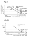
- Fig. 28 shows a characteristic of the integral signal ⁇ V MN dt relative to the phase correction angle when the load is varied with the running frequency kept constant in the above-mentioned brushless DC motor system.
- the characteristic of the above-mentioned brushless DC motor system exhibits an approximately straight line where the level of the integral signal ⁇ V MN dt gradually reduces from the lead correction side to the lag correction side of the phase correction angle.
- the line shifts to the lead correction side of the phase correction angle according as the load increases, and the line shifts approximately parallel from the lead correction side to the lag correction side of the phase correction angle according as the load decreases.
- the level of the integral signal ⁇ V MN dt is V2.
- the level of the integral signal ⁇ V MN dt is V3.
- Fig. 29 shows a characteristic of the integral signal ⁇ V MN dt relative to the phase correction angle when the running frequency is varied with the load kept constant in the above-mentioned brushless DC motor system.
- the characteristic of the above-mentioned brushless DC motor system exhibits an approximately straight line where the level of the integral signal ⁇ V MN dt gradually reduces from the lead correction side to the lag correction side of the phase correction angle.
- the line shifts to the lead correction side of the phase correction angle according as the running frequency increases, and the line shifts approximately parallel from the lead correction side to the lag correction side of the phase correction angle according as the running frequency decreases.
- the level of the integral signal ⁇ V MN dt is V4.
- the level of the integral signal ⁇ V MN dt is V5.
- the present invention is applied to a brushless DC motor system in which the level of the integral signal is not constant at the peak efficiency point depending on the magnitude of the load and the pitch of the running frequency.
- the level detection signal switching section 102 outputs a switching signal to the switch SW. That is, according to the variation of the load and the variation of the running frequency, one of the level detectors 6A, 6B, ..., is selected and a reference value for deciding the level of the integral signal ⁇ V MN dt is changed. Subsequently, the microcomputer 100 executes an interrupt handling process as shown in the flow charts of Figs. 12, 13, 14 and 15 of the first embodiment. The level decision section 101 adjusts the phase correction angle so that the peak motor efficiency is achieved, and outputs a phase correction angle command signal. Therefore, the motor can be operated at the peak efficiency regardless of the magnitude of the load and the pitch of the running frequency.
- Fig. 30 shows a block diagram of a microcomputer employed in a brushless DC motor system of a third embodiment of the present invention.
- the brushless DC motor system has the same construction as that of the brushless DC motor system shown in Fig. 7 except for the microcomputer and the level detector. There is provided no description for the components except for a microcomputer 200 and an A/D converter 202 which substitutes for the level detector.
- the A/D converter 202 Upon receiving the integral signal from the rotational-position sensor 3, the A/D converter 202 outputs an integral signal which has undergone an analog to digital conversion process.
- the above-mentioned brushless DC motor system includes a level decision section 201 which receives the position signal from the rotational-position sensor 3, the current speed signal from the speed calculator 44, an external torque signal representing a load torque value, and the integral signal which has undergone the analog to digital conversion process, and outputs a phase correction angle command signal to the timer value calculator 42.
- the level of the integral signal is not made constant at the peak efficiency point in accordance with the magnitude of the load and the pitch of the running frequency similarly to the second embodiment.
- the level decision section 201 selects a target value from a preset table based on the current speed signal from the speed calculator 44 and the external torque signal, and decides whether or not the peak value of the integral signal which has undergone the analog to digital conversion process is not smaller than the target value. Then, an interrupt handling process shown in the flow charts of Figs. 12 through 15 is executed to adjust the phase correction angle so that the peak motor efficiency is achieved, and a phase correction angle command signal is outputted.
- the motor can be operated at the peak efficiency regardless of the magnitude of the load and the pitch of the running frequency.
- Fig. 31 shows a construction of a brushless DC motor system of a fourth embodiment of the present invention.
- Reference numeral 301 denotes a stator which has star-connected armature coils 301a, 301b and 301c, and rotates a rotor 310 having a plurality of permanent magnets by a rotating magnetic field.
- Reference numeral 302 denotes a resistor circuit which is comprised of star-connected resistors 302a, 302b and 302c and connected in parallel with the armature coils 301a, 301b and 301c.
- Reference numeral 303 denotes an integral signal detector which detects the voltage difference signal V MN representing the voltage difference between the voltage V M at the neutral point of the resistor circuit 302 and the voltage V N at the neutral point of the armature coils 301a, 301b and 301c, integrates the voltage difference signals V MN , and outputs the integral signal ⁇ V MN dt.
- Reference numeral 304 denotes a microcomputer which receives the integral signal from the integral signal detector 303 and outputs a switching signal.
- Reference numeral 305 denotes a base drive circuit which receives the switching signal from the microcomputer 304 and outputs a commutation control signal. The commutation control signal from the base drive circuit 305 is inputted to an inverter section 320.
- the stator 301 and the rotor 310 constitute a brushless DC motor 311.
- Fig. 32 is a block diagram of the microcomputer 304.
- the microcomputer 304 has the same construction as that of the first embodiment. Therefore, the same components are denoted by the same reference numerals, and no description is provided therefor.
- the integral signal detector 303 includes a differential amplifier 331 in which the voltage V M at the neutral point of the resistor circuit 302 is inputted to a non-inverted input terminal of an amplifier IC111, a ground GND is connected to an inverted input terminal of the amplifier IC111 via a resistor R 111 , and a resistor R 112 is connected between an output terminal and an inverted input terminal of the amplifier IC111; and an integrator 332 comprised of a resistor R 113 of which one end is connected to the output terminal of the differential amplifier 331 and a capacitor C 111 connected between the other end of the resistor R 113 and the ground GND.
- the neutral point of the armature coils 301a, 301b and 301c is connected to the inverted input terminal of the differential amplifier 331 via the ground GND and the resistor R 111 . Therefore, the differential amplifier 331 detects the voltage difference signal V MN representing the voltage difference between the voltage V M at the neutral point of the resistor circuit 302 and the voltage V N at the neutral point of the armature coils 301a, 301b and 301c.
- the above-mentioned brushless DC motor system further includes a level detector 306 which receives the integral signal ⁇ V MN dt from the integrator 332 of the integral signal detector 303, and outputs a level detection signal to the microcomputer 304.
- the level detector 306 shown in Fig. 33 the integral signal ⁇ V MN dt from the integrator 332 is inputted to an inverted input terminal of an amplifier IC121 via a resistor R 121 , and a non-inverted input terminal of the amplifier IC121 is connected to the ground GND.
- an anode of a diode D 101 is connected to an output terminal of the amplifier IC121, and a cathode of the diode D 101 is connected to the inverted input terminal of the amplifier IC121.
- a cathode of a diode D 102 is connected to the output terminal of the amplifier IC121, and an anode of the diode D 102 is connected to the inverted input terminal of the amplifier IC121 via a resistor R 122 .
- An inverted input terminal of an amplifier IC122 is connected to a connection point of the anode of the diode D 102 and the resistor R 122 via a resistor R 123 .
- a resistor R 124 is connected between the inverted input terminal of the amplifier IC122 and an end on the integral signal ⁇ V MN dt input side of the resistor R 121 , while a non-inverted input terminal of the amplifier IC122 is connected to the ground GND.
- An inverted input terminal of a comparator IC123 is connected to the output terminal of the amplifier IC122 via a resistor R 126 , and connected to the ground GND via a capacitor C 101 .
- a non-inverted input terminal of the comparator IC123 is connected to a power supply via a resistor R 127 , and connected to the ground GND via a resistor R 128 .
- the resistor R 127 and the resistor R 128 define a reference value E3 for the comparator IC123.
- the above-mentioned brushless DC motor system includes Hall elements 312a, 312b and 312c which detect the rotational position of the rotor 310 by a magnetic field exerted from the magnets of the rotor 310 of the motor 311, and a rotational-position sensor 313 which serves as rotational-position sensor means and operates to receive output signals from the Hall elements 312a, 312b and 312c and output a position signal representing the rotational position of the rotor 310.
- the rotational-position sensor 313 includes an amplifier IC112 for amplifying the output signal from the Hall element 312a; an amplifier IC113 for amplifying the output signal from the Hall element 312b; an amplifier IC114 for amplifying the output signal from the Hall element 312c; an OR-circuit OR1 to which both the output signals of the amplifiers IC112 and IC114 are input; an OR-circuit OR2 to which both the output signals of the amplifiers IC112 and IC113 are input; an OR-circuit OR3 to which both the output signals of the amplifiers IC113 and IC114 are input; and an AND-circuit AND1 which receives output signals of the OR-circuits OR1, OR2 and OR3 and outputs the position signal.
- the level detector 306 subjects the integral signal ⁇ V MN dt to full-wave rectification (shown in Fig. 35 (G)) by means of a full-wave rectifier comprised of the diodes D 101 and D 102 , the resistors R 121 through R 126 , and amplifiers IC121 and IC122. Then the full-wave rectified signal is smoothed by a smoothing circuit comprised of the resistor R 126 and the capacitor C 101 . Thereafter, the smoothed signal (shown in Fig. 35 (H)) is compared with the reference value E3 in the comparator IC123, and a level detection signal (shown in Fig.
- the level detection signal is made to have H-level when the level of the smoothed signal is not greater than the reference value E3, and the level detection signal is made to have L-level when the level of the smoothed signal exceeds the reference value E3.
- Fig. 34 shows an interrupt handling process 11 of the microcomputer 304 which executes the same operation as that of the flow charts of Figs. 13, 14 and 15 except for the flow chart of Fig. 34. It is to be noted that the interrupt handling process 11 is executed at every rise time and fall time of the position signal inputted to the external interrupt terminal of the microcomputer 304.
- step S201 it is decided whether or not the level detection signal is at L-level at step S201.
- step S221 at which the preceding phase correction angle command is incremented by one degree (to the lag correction side), and the program flow proceeds to step S104 shown in Fig. 13.
- step S222 at which the preceding phase correction angle command is decremented by one degree (to the lead correction side), and the program flow proceeds to step S104 shown in Fig. 13.
- the motor can be operated at the peak efficiency regardless of the magnitude of the load and the pitch of the running frequency similarly to the first embodiment. Furthermore, by gradually adjusting the phase of the voltage pattern from the lead correction side to the lag correction side so as to achieve the peak motor efficiency point, the phase of the voltage pattern is prevented from being adjusted to a step-out region existing on the lag correction side of the peak efficiency point. Therefore the step out is prevented.
- Fig. 36 shows a block diagram of a microcomputer of a brushless DC motor system of an fifth embodiment of the present invention.
- the present brushless DC motor system has the same construction as that of the brushless DC motor system of the fourth embodiment shown in Fig. 31 except for a microcomputer 308 and a level detector 307 (see Fig. 37), and there is provided no description therefor.
- the microcomputer 308 has the same construction as that of the microcomputer 304 of the fourth embodiment shown in Fig. 32 except for a read timer 60, and the same components are denoted by the same reference numerals, and no description is provided therefor.
- the level detector 307 includes an amplifier IC131 where the integral signal ⁇ V MN dt from the integrator 332 is inputted to an inverted input terminal thereof, a non-inverted input terminal thereof is connected to the ground GND via a resistor R 131 , and an output terminal and the non-inverted input terminal thereof are connected to each other via a resistor R 132 .
- the amplifier IC131 and the resistors R 131 and R 132 constitute a hysteresis comparator having a hysteresis characteristic.
- the output terminal of the amplifier IC131 comes to have H-level when the integral signal ⁇ V MN dt becomes smaller than a reference value E5. That is, the level detection signal (shown in Fig. 38 (G)) of the level detector 307 becomes a signal which has a phase different from that of the position signal (shown in Fig. 38 (D)) and a cycle identical to the position signal.
- the level of the integral signal ⁇ V MN dt from the integrator 332 becomes low, there is a possibility that the integral signal ⁇ V MN dt does not exceed the reference value E4 or the possibility that the integral signal ⁇ V MN dt does not become smaller than the reference value E5.
- the level detection signal comes to have a frequency smaller than that of the position signal, and a duty ratio different from that of the position signal.
- decision as to whether or not the integral signal ⁇ V MN dt has a level not smaller than a specified level can be done through the discrimination whether or not the level detection signal is continuous in a specified cycle.
- step S301 when the interrupt handling process 21 starts, it is decided whether or not a preceding-time level detection signal is at H-level at step S301.
- the program flow proceeds to step S321 to decide whether or not a current-time level detection signal is at L-level.
- step S322 the program flow proceeds to step S322 to increment a counter CNT1 by one.
- step S302 the program flow proceeds to step S302.
- step S323 At which it is decided whether or not the current-time level detection signal is at H-level.
- step S324 the program flow proceeds to step S324 to increment the counter CNT1 by one.
- a counter CNT2 is incremented by one at step S302, and the program flow proceeds to step S303. Then, it is decided whether or not the counter CNT2 indicates 3 at step S303. When it is decided that the counter CNT2 indicates 3, the program flow proceeds to step S325. When it is decided that the counter CNT2 does not indicate 3, the program flow proceeds to step S304 shown in Fig. 40. Then, it is decided whether or not the counter CNT1 indicates 3 at step S325. When it is decided that the counter CNT1 indicates 3, the program flow proceeds to step S326 to increment by one degree the preceding-time phase correction angle command (to the lag correction side), and the program flow proceeds to step S329.
- step S327 decides whether or not the counter CNT1 indicates 0.
- step S328 decrement by one degree the preceding-time phase correction angle command (to the lead correction side), and the program flow proceeds to step S329.
- step S329. the program flow proceeds to step S329.
- step S330 the program flow proceeds to step S330 to clear the counter CNT2, and proceeds to step S304. It is to be noted that before the initial interrupt handling process 21 starts, an initial value is set to the phase correction angle command and the counters CNT1 and CNT2 are cleared.
- step S304 shown in Fig. 40 it is decided whether or not the phase correction timer T1 (referred to as a timer T1 in Fig. 40) is counting.
- the program flow proceeds to step S331 to stop the timer T1. That is, when the timer T1 is counting, the timer T1 is stopped to get ready for the next start.
- a voltage pattern is outputted at step S332, and the program flow proceeds to step S305.
- the program flow proceeds to step S305.
- a correction angle (phase correction angle based on the phase correction command signal from the level decision section 51) is not smaller than 60 degrees.
- the program flow proceeds to step S341 to decide whether or not the correction angle is not smaller than 120 degrees.
- the program flow proceeds to step S342 to establish a phase correction E (referred to as a "correction E” in Fig. 40), and proceeds to step S343.
- it is decided whether or not the preceding phase correction is a phase correction C (referred to as a "correction C" in Fig. 40) or a phase correction D (referred to as a "correction D" in Fig.
- step S343 When it is decided that the preceding phase correction is the phase correction C or the phase correction D, the program flow proceeds to step S344 to issue a correction switching request, and thereafter proceeds to step S306. When it is decided that the preceding phase correction is neither the phase correction C nor the phase correction D at step S343, the program flow proceeds to step S306.
- step S345 to establish the phase correction D, and proceeds to step S346.
- step S346 it is decided whether or not the preceding phase correction is the phase correction C or the phase correction E at step S346.
- the program flow proceeds to step S347 to issue a correction switching request, and thereafter proceeds to step S306.
- step S306 it is decided that the preceding phase correction is neither the phase correction C nor the phase correction E at step S346, the program flow proceeds to step S306.
- step S351 to establish the phase correction C, and proceeds to step S352.
- step S352 it is decided whether or not the preceding phase correction is the phase correction D or the phase correction E at step S352.
- the program flow proceeds to step S353 to issue a correction switching request, and thereafter proceeds to step S306. Otherwise, when it is decided that the preceding phase correction is neither the phase correction D nor the phase correction E at step S352, the program flow proceeds to step S306.
- a timer value TISOU is calculated every time of phase corrections C, D and E. That is, in the phase correction C, a timer value corresponding to the phase correction angle is set as the timer value TISOU. In the phase correction D, a timer value corresponding to a phase angle obtained by subtracting 60 degrees from the phase correction angle is set as the timer value TISOU. In the phase correction E, a timer value corresponding to a phase angle obtained by subtracting 120 degrees from the phase correction angle is set as the timer value TISOU. Then, the program flow proceeds to step S307 to increment the inverter mode by one step.
- step S308 shown in Fig. 41 at which it is decided whether or not the correction switching request has been issued.
- the program flow proceeds to step S361 to decide whether the correction mode is switched from the phase correction C (referred to as a "correction C" in Fig. 41) to the phase correction D (referred to as a “correction D” in Fig. 41) or from the phase correction D to the phase correction E (referred to as a "correction E” in Fig. 41).
- step S362 When it is decided that the correction mode is switched from the phase correction C to the phase correction D or from the phase correction D to the phase correction E, the program flow proceeds to step S362 to cancel the correction switching request, the inverter mode is put back by one step at step S362-1, and the program flow proceeds to step S309.
- step S363 when the correction mode is switched neither from the phase correction C to the phase correction D nor from the phase correction D to the phase correction E, i.e., switched from the phase correction D to the phase correction C or from the phase correction E to the phase correction D, the program flow proceeds to step S363 to output a voltage pattern. Then, the program flow proceeds to step S364 to set the timer value TISOU calculated at step S306 to the timer T1, and thereafter the timer T1 is started at step S365. Then, the program flow proceeds to step S366 to cancel the correction switching request, and proceeds to step S309.
- step S368 When it is decided that there is no correction switching request at step S308, the program flow proceeds to step S368 to set the timer value TISOU calculated at step S306 to the timer T1, the timer T1 is started at step S369, and the program flow proceeds to step S309.
- step S309 the cycle measuring timer T2 is stopped and a timer value in the cycle measuring timer T2 is read at step S309, and the program flow proceeds to step S310.
- the cycle measuring timer T2 is set and started at step S310 to start the next cycle measurement.
- a cycle calculation is executed from the value of the cycle measuring timer T2 in the cycle calculator 41 at step S311, and from the calculation result, the rotation speed of the motor is calculated in the speed calculator 44.
- the speed controller 45 executes speed control based on an external speed command signal to output a voltage command signal at step S112.
- the signal is read through the aid of the read timer 60 shown in Fig. 36. That is, the read timer 60 is started at a rise time and a fall time of the position signal from the rotational-position sensor 113.
- the read timer 60 outputs a read signal (shown in Fig. 38 (E)) to the level decision section 51.
- the level decision section 51 receives the read signal, an interrupt handling process 23 as shown in Fig. 42B starts.
- the level detection signal is read (it is decided whether the level of the level detection signal is at L-level or H-level by the level decision section 51) at step S380 of the interrupt handling process 23, and thereafter the interrupt handling process 23 ends.
- the motor can be operated at the peak efficiency regardless of the magnitude of the load and the pitch of the running frequency. Furthermore, by gradually adjusting the phase of the voltage pattern from the lead correction side to the lag correction side so as to achieve the peak motor efficiency point, the phase of the voltage pattern is prevented from being adjusted to a step-out region existing on the lag correction side of the peak efficiency point. Therefore the step out can be prevented.
- Fig. 43 shows a construction of an AC (Alternating Current) motor system of a sixth embodiment of the present invention.
- Reference numeral 401 denotes a stator which has star-connected armature coils 401a, 401b and 401c and rotates a rotor 410 by a rotating magnetic field.
- Reference numeral 402 denotes a resistor circuit which is comprised of star-connected resistors 402a, 402b and 402c and is connected in parallel with the armature coils 401a, 401b and 401c.
- Reference numeral 403 denotes a differential amplifier which detects the voltage difference signal representing the voltage difference between a voltage V M at a neutral point of the resistor circuit 402 and a voltage V N at a neutral point of the armature coils 401a, 401b and 401c.
- Reference numeral 404 denotes an integrator which receives the voltage difference signal from the differential amplifier 403 and integrates the voltage difference signal.
- Reference numeral 405 denotes an RMS (Root Mean Square) converter which receives the integral signal from the integrator 404 via a transformer PT and obtains an RMS value of the integral signal from which DC components are removed.
- RMS Root Mean Square
- Reference numeral 406 denotes a microcomputer which receives a signal representing the RMS value of the integral signal from the RMS converter 405 and outputs a switching signal.
- Reference numeral 407 denotes a base drive circuit which receives the switching signal from the microcomputer 406 and outputs a commutation control signal.
- the commutation control signal from the base drive circuit 407 is inputted to an inverter section 420.
- the stator 401 and the rotor 410 constitute an AC motor 411.
- Fig. 44 is a schematic block diagram of the microcomputer 406.
- the microcomputer 406 includes an acceleration/deceleration processor 501 which receives a frequency command signal f1* and outputs a signal f1 representing an inverter output frequency; a voltage processor 502 which receives the signal f1 representing the inverter output frequency from the acceleration/ deceleration processor 501 and a neutral-point voltage vn, and outputs a signal vo representing an inverter output voltage; and a sine-wave PWM processor 503 which receives the output frequency signal f1 obtained by the acceleration/deceleration processor 501 and the signal vo representing the inverter output voltage from the voltage processor 502, and outputs a commutation control signal.
- an acceleration/deceleration processor 501 which receives a frequency command signal f1* and outputs a signal f1 representing an inverter output frequency
- a voltage processor 502 which receives the signal f1 representing the inverter output frequency from the acceleration/ decel
- Fig. 45 shows a flow chart of a processing operation of the microcomputer 406.
- An interrupt handling process 31 of the microcomputer 406 will be described below with reference to Fig. 45. It is to be noted that the interrupt handling process 31 is processed by an interrupt signal generated every 0.1 to 1 second from a timer (not shown).
- a current-time value f1 of the inverter frequency and a current-time value vn(i) of the neutral-point voltage, i.e., the effective value of an integral signal obtained by the RMS converter 405 are respectively inputted at step S401.
- the inverter output voltage vo(i) is calculated at step S402 according to the following equation.
- step S403 it is decided whether or not a minimum value vomin (f1) of the inverter output voltage is greater than the inverter output voltage vo(i) at step S403.
- the program flow proceeds to step S406 to make the inverter output voltage vo(i) assume the minimum value vomin(f1), and thereafter the program flow proceeds to step S404.
- the program flow proceeds to step S404. That is, as shown in Fig. 46, the minimum value vomin of the inverter output voltage is approximately proportional to the inverter frequency f1, and the inverter output voltage vo(i) obtained at step S402 is made to be not smaller than the minimum value vomin.
- a value of the preceding sample is stored at step S404. That is, the inverter output voltage vo(i) is substituted into the inverter output voltage vo(i-1), and the current-time value Vn(i) of the neutral-point voltage is substituted into the neutral-point voltage Vn(i-1).
- Fig. 48 shows a graph obtained through an experiment of characteristics of an efficiency ⁇ of the AC motor and the neutral-point voltage RMS value vn relative to the inverter output line voltage vo when the inverter frequency f1 is 30 Hz and the torque is set at 10 kgfcm, 15 kgfcm and 20 kgfcm. From the result of the experiment, it can be found that characteristic curves of the neutral-point voltage each have an approximately minimum value at a point corresponding to the peak point of the efficiency ⁇ of the AC motor.
- the AC motor is operated at the peak efficiency.
- the rotation speed is controlled by adjusting the inverter output voltage
- the optimum efficiency control by which the motor is operated at the peak efficiency is achieved by adjusting the phase of the voltage pattern of the inverter output.
- a brushless DC motor is used in the first through fifth embodiments, and an AC motor is used in the sixth embodiment.
- the present invention is not limited to this, and the present invention can be of course applied to a reluctance motor or the like.
- the peak-efficiency operation is performed by adjusting the phase correction angle so that the level of the integral signal becomes the target value at the peak efficiency point.
- the above-mentioned operation can be performed so that the level of the voltage difference signal becomes the target value at the peak efficiency point.
- the motor can be operated at an arbitrary efficiency by using the above-mentioned integral signal or the voltage difference signal and setting a target value at the arbitrary efficiency.
- phase correction timer T1 the cycle measuring timer T2, the cycle calculator 41 and the timer value calculator 42 are used as the phase correction means.
- the phase correction means is of course not limited to this.
- the microcomputer 4 (14, 100, 200, 304, 308 and 406) is used.
- a logic circuit and so forth can be used instead of the microcomputer.
- the voltage pattern switching system of the armature coils 1a, 1b and 1c(301a, 301b and 301c) is implemented by the 180° conduction system.
- the voltage pattern switching is not limited to the 180° system, and it may be a conduction system of 120 to 180°.
- the rotational-position sensor 3 is used as the rotational-position sensor means.
- the rotational-position sensor means is not limited to this, and another circuit construction can be of course adopted.
- the rotational-position sensor means can be implemented by a circuit shown in Fig. 49, including an amplifier IC21 where the voltage V M at the neutral point of the resistor circuit 2 is inputted to an inverted input terminal thereof, a resistor R 21 is connected between a non-inverted input terminal thereof and the ground GND, and a resistor R 22 and a capacitor C 21 are connected in parallel with each other between an output terminal thereof and the inverted input terminal; and an amplifier IC22 where an inverted input terminal thereof is connected to the output terminal of the amplifier IC21, a resistor R 23 is connected between a non-inverted input terminal thereof and the ground GND, and a resistor R 24 is connected between an output terminal thereof and the non-inverted input terminal.
- the rotational-position sensor means can be achieved by a circuit as shown in Fig. 50 including an amplifier IC31 where the voltage V M at the neutral point of the resistor circuit 2 is inputted to an inverted input terminal thereof, a resistor R 31 is connected between a non-inverted input terminal thereof and the ground GND, and a resistor R 32 is connected between an output terminal thereof and the inverted input terminal; an amplifier IC32 where an inverted input terminal thereof is connected to the output terminal of the amplifier IC31 via a resistor R 33 , a resistor R 34 is connected between a non-inverted input terminal thereof and the ground GND, and a resistor R 35 and a capacitor C 31 are connected in parallel with each other between an output terminal thereof and the inverted input terminal; and an amplifier IC33 where an inverted input terminal thereof is connected to the output terminal of the amplifier IC32, a resistor R 36 is connected between a non-inverted input terminal thereof and the ground GND, and a resistor R 37 is connected between an output terminal thereof and the
- the rotational position sensor means can be constructed as a circuit which includes an amplifier IC41 where a voltage V N at the neutral point of the armature coils 1a, 1b and 1c is inputted to an inverted input terminal thereof via a resistor R 41 , a voltage V M
- the integral signal ⁇ V MN dt is subjected to an analog to digital conversion process.
- a voltage difference signal, a signal obtained by smoothing the voltage difference signal, or a signal obtained by smoothing the integral signal ⁇ V MN dt is also practicable to subject a voltage difference signal, a signal obtained by smoothing the voltage difference signal, or a signal obtained by smoothing the integral signal ⁇ V MN dt to an analog to digital conversion process, and perform the level decision using the signal obtained through the analog to digital conversion process.
- the number of times of counting of the level detection signal is five in the first embodiment, and three in the fifth embodiment.
- the number of times of counting can be an arbitrary number.
- the integrator 22 of the rotational-position sensor 3 is used as an integration means in the first embodiment, however, the integration means can be constructed independently of the integrator of the rotational-position sensor.
- the rotational position of the rotor 10 is detected by the rotational-position sensor 3 which serves as the rotational-position sensor means in the first through third embodiments, and the rotational position of the rotor 10 is detected by the Hall elements 312a, 312b and 312c and the rotational-position sensor 313 in the fourth and fifth embodiments, however, the rotational-position sensor means is not limited to these.
- the rotational-position sensor means is not limited to these.
- the brushless DC motors and other motors as well as their control methods according to the present invention are suited for use in household electrical appliances such as inverter air conditioners and other air conditioners, electric washers, and vacuum cleaners.
Description
- The present invention relates to a motor system capable of high efficiency operation.
- Brushless DC motors have conventionally been researched and developed for their application to various fields, and also put into practical use, taking advantage of their capability that no secondary copper loss is involved so that enhancement in efficiency is theoretically possible.
- The methods for controlling brushless DC motors to high efficiency can be classified roughly into the following two:
- (i) A method in which the motor current is controlled so that the torque-to-current ratio is increased, by detecting the instantaneous value of the motor current; and
- (ii) A method in which a rotation speed of the motor is detected and the voltage-fed inverter is controlled in response to the detected rotation speed so that the inverter output voltage relative to the phase of the motor counter-electromotive voltage is brought to a phase that allows the brushless DC motor to be driven at around the maximum output.
-
- In the above (i) method, when a brushless DC motor in which a permanent magnet is mounted on the surface of the rotor (hereinafter, referred to as surface-magnet DC motor) is adopted, the motor current is controlled so that the d-axis current (a current in the same direction as that of the gap magnetic flux) that is irrelevant to torque generation is reduced to zero (see "Theory and Practical Design of AC servo systems," Sugimoto et al., published by Sogodenshi Shuppansha K.K., p. 74). Also, when a brushless DC motor in which a permanent magnet is mounted so as to be buried inside the rotor (hereinafter, referred to as buried-magnet DC motor) is adopted, the motor current is controlled based on the fact that the generated torque is the sum of magnet torque (a torque proportional to the q-axis current, which is a current in a direction perpendicular to that of gap magnetic flux) and reluctance torque (a torque proportional to the product of d- and q-axis currents), in such a way that optimum values for the d- and q-axis currents are obtained through the steps of detecting the load status (torque) and sequentially performing arithmetic operations to calculate the optimum values of the d- and q-axis currents (see "High Efficiency Control of Brushless DC Motors for Energy Saving," Morimoto et al., T.IEE Japan, Vol. 112-D, No. 3, '92, in particular, Equations (14) and (15)).
- The method (i) allows easy application to such fields as would demand high-speed torque response, for example, brushless DC motor drive systems used in machine tools, industrial robots, and the like, where a voltage-fed inverter is previously provided with an instantaneous current detector to implement a high-speed current control system so that there is no need of providing a special device for high efficiency. It is because the current response becomes generally equal to the torque response in brushless DC motors that the high-speed current control system is implemented. This allows a high-speed torque response to be realized.
- Meanwhile, the brushless DC motor drive system in household electrical appliances such as air conditioners, washers, and cleaners is based on a simple control system in which the voltage waveform is controlled by only a voltage-fed inverter in response to a position signal derived from detecting the position of the rotor of the brushless DC motor. Therefore, the above (i) method, if applied, would make it necessary not only to newly provide an instantaneous current detector but also to enhance the control operation function, particularly when a buried-magnet DC motor is adopted. As a result, a high-performance microcomputer needs to be substituted for or be added to an existing microcomputer, which incurs a great increase in cost.
- In view of these and other problems, it has been proposed to adopt such a constitution for brushless DC motor drive systems in household electrical appliances such as air conditioners, washers, and cleaners that the voltage-fed inverter is controlled so that the phase of the inverter output voltage relative to the phase of the motor counter-electromotive voltage will be set to a specified phase in response to a rotation speed of the brushless DC motor, in addition to the simple control system in which the voltage waveform is controlled by only a voltage-fed inverter in response to a position signal resulting from detecting the rotor position of the brushless DC motor. Adopting this constitution involves neither an instantaneous current detector nor a high-performance microcomputer, so that the aforementioned increase in cost can be largely reduced.
- As described above, with the constitution that the voltage-fed inverter is controlled so that the phase of the inverter output voltage relative to the phase of the motor counter-electromotive voltage will be set to a specified phase in response to a rotation speed of the brushless DC motor, the motor is enabled to attain high-efficiency operation as far as the operation is limited to around the rated point. However, the motor generally runs quite away from the rated point considerably longer than it does around the rated point. In the operation during the former period, the current value would not lower even if the voltage amplitude is reduced with a less load, so that a current more than necessary would be passed. As a result, the motor can be operated only at efficiencies lower than its best possible efficiency (peak efficiency at different load conditions) to a disadvantage.
- In more detail, if a buried-magnet DC motor with a d-axis inductance Ld of 65 mH and a q-axis inductance Lq of 15.0 mH and a counter-electromotive voltage coefficient Ke of 0.105 Vs/rad is driven at a rotation speed 90 rps., and if the phase of the motor counter-electromotive voltage and the phase of the inverter output voltage are set to 50° and 80°, respectively, then it can be understood from Fig. 1, which charts the motor output characteristic and motor current characteristic relative to the line voltage amplitude of the voltage-fed inverter, that although a brushless DC motor can be operated at larger output with larger settings of phase δ, the current value would show almost no decrease even if the line voltage amplitude of the voltage-fed inverter (amplitude of fundamental wave components) is reduced with lighter loads.
- Also, when the peak motor efficiency at different rotation speeds was measured with the load set to 10 kgf·cm and the phase δ adjusted by manual operation, a characteristic as marked by white circles in Fig. 2 was obtained. In contrast, when the motor efficiency with a low load at different rotation speeds was measured with a phase δ that is optimum for a high load (20 kgf·cm), a characteristic as marked by white triangles in Fig. 2 was obtained. Therefore, it can be understood that the motor efficiency lowers to a large extent when the motor is operated with a light load. Further, the larger the winding resistance is, the more noticeably the motor efficiency lowers.
- Fig. 3 is a block diagram schematically showing the arrangement of a conventional brushless DC motor system, and Fig. 4 is a block diagram showing the main part of the control circuit in Fig. 3. As shown in Fig. 3, the conventional brushless DC motor system is so arranged that an AC voltage 91 is converted into a DC voltage by a converter 92a of a voltage-fed inverter 92 and thereafter converted into an AC voltage by an inverter main part 92b and, as such, supplied to a brushless DC motor 93, where the magnetic-pole position of the rotor of the brushless DC motor 93 is detected by a position sensor circuit 94 and a switching command is generated by a control circuit 96 in response to a magnetic-pole position detection signal and then fed to the voltage-fed inverter 92.
- Also, as shown in Fig. 4, the control circuit 96 comprises an amplitude command output section 96a for receiving inputs of, for example, an actual rotation speed and a rotation speed command, which are obtained based on the time interval of magnetic-pole position detection signals outputted by the position sensor circuit 94, and a phase table 96b for outputting a phase command corresponding to the actual rotation speed by taking the actual rotation speed as a read address, whereby an amplitude command and a phase command are fed to an unshown PWM circuit so that a switching command is generated.
- The amplitude command output section 96a calculates, for example, a difference ΔY between a rotation speed command Y* and an actual rotation speed Y, and performs a PI operation of V* = Kp·ΔY + KI·σ(ΔY) by using the resulting difference ΔY, thereby determining and outputting an amplitude command V*, where Kp and KI are each a constant and given by, for example, values obtained experientially.
- Therefore, a switching command is generated by feeding the amplitude command V* calculated from the difference between rotation speed command Y* and actual rotation speed Y as well as a phase command read from the phase table 96b to the PWM circuit, whereby the actual rotation speed Y can be approached and equalized to the rotation speed command Y*.
- However, when the above-described brushless DC motor control circuit is adopted, the motor efficiency with light loads would deteriorate to a large extent. Also, over the high-speed region in which the induced voltage of the brushless DC motor with no loads becomes larger than the inverter output voltage amplitude (a region in which the motor induced voltage is suppressed from increasing by utilizing the stator-to-armature reaction, that is, magnetic-flux weakening control is effected), the motor could not be controlled in such a way that the motor current is minimized by fixing the inverter voltage at a maximum.
- These points are now described in more detail.
- Fig. 5 shows an equivalent circuit of one phase portion of the brushless DC motor. As shown in the figure, this equivalent circuit has a motor winding resistance R, a reactance Xq on the q-axis, and an induced voltage (more precisely, a voltage resulting from adding the product of a difference between q-axis reactance Xq and d-axis reactance Xd and a d-axis component Id of motor current to the counter-electromotive voltage E) connected in series with the inverter fundamental-wave voltage V in this order. It is noted that j in Fig. 5 represents an imaginary number.
- In this arrangement, assuming that the frequency of inverter fundamental wave is ω (where the number of revolutions is ω/n in the case of a brushless DC motor with n pairs of magnetic poles), the inductances on the d- and q-axes are Ld and Lq, respectively, the counter-electromotive voltage coefficient is Ke, the motor current is I, the d-axis component and q-axis component of the motor current I are Id and Iq, respectively, the output torque is T, the d-axis component and q-axis component of the inverter fundamental-wave voltage V are Vd and Vq, respectively, and that the motor winding resistance R is substantially smaller than the magnitude |X| of the reactance, then the following relational equations are obtained:
- Then, on a brushless DC motor with motor constants Ld = 6.5 mH, Lq = 15.0 mH, Ke = 0.15 V·s/rad, when the output torque and the amplitude of motor current were calculated while the inverter fundamental-wave voltage amplitude |V| {= (Vd2+Vq2)1/2} was varied, results as shown in Figs. 6A and 6B were obtained, where the number n of motor pole pairs was 2 and the rotation speed was set to 90 rps.
- As apparent from Figs. 6A and 6B, such a reciprocal relationship is shown that the motor current amplitude increases even if the output torque T is decreased. That is, the joule loss of motor windings becomes greater with a light load (i.e., with a small output torque) than it is with a heavy load, so that the efficiency would lower considerably. Also, since the motor current amplitude becomes quite large with a light load, switching devices and the like with greater current capacities must be adopted as those constituting the voltage-fed inverter.
- Further, since the rotation speed of the brushless DC motor is controlled by adjusting the voltage amplitude of the voltage-fed inverter (PWM duty factor), the phase is fixed so that the voltage amplitude command will not be saturated at the time of acceleration in order to stably operate the speed control system. As a result, it is impossible to set such a phase that the voltage amplitude of the inverter is maximized at a constant speed. In other words, it is necessary to ensure margins for voltage amplitude adjustment at all times. Accordingly, it is impossible to perform such control that the motor current is minimized with the steady-state voltage amplitude of the voltage-fed inverter fixed at a maximum.
- The above-described disadvantages would be involved similarly in both cases of brushless DC motors in which a permanent magnet is disposed inside the rotor (buried-magnet motors), and brushless DC motors in which a permanent magnet is disposed on the surface of the rotor (surface-magnet motors).
- EP-A1-0 589 630 discloses a circuit and method for automatically adjusting a commutation delay from events indicating a position of a polyphase dc motor. The circuit includes a driver to supply drive current to selected stator coils of said motor. A sequencer is connected to control the driver to apply drive current to selected motor coils to rotate the motor. Motor position detecting circuitry is connected to detect the events indicating the position of the motor. A commutation delay circuit is connected to increment the sequencer in response to the detection of the events indicating the position of the motor detected by the motor position detecting circuitry. A circuit for adjusting the delay of said commutation delay circuit between each event and each sequencer commutation provides optimum motor commutation for maximum power efficiency.
- According to the method, drive current is supplied to selected stator coils of said motor in predetermined commutated sequences to rotate the motor. Events are detected indicating the position of the motor, and the delay between each position indicating event and each commutation sequence is automatically adjusted to provide optimum motor commutation for maximum power efficiency.
- US-A-4 641066 discloses a control apparatus which detects a suitable starting point during rotational oscillation of a rotor at the start of a brushless motor by combining the polarity of a counter electromotive force generated in an armature coil of an armature winding of the brushless motor for a nonexcited phase due to the rotational oscillation of the rotor (when armature coils for particular phases are excited at the start of the brushless motor) with the pulse edge of an excitation switchover signal obtained from the potential of a neutral point of the armature winding having the armature coils connected in star-connection and that of a neutral point of a detecting resistance circuit having resistors connected in star-connection. Each of the resistors of the resistance circuit is arranged in parallel with a corresponding one of the armature coils of the armature winding. By driving the brushless motor from the detected suitable starting point, it is possible to effect smooth and quick control of the starting operation of the brushless motor.
- The present invention has been achieved in view of the aforementioned problems.
- An object of the present invention is to provide a motor system (DC or AC motor system) which can be operated at peak efficiency while the motor can be prevented from stepping out.
- The present invention provides a motor system according to independent claims 1 and 2. Preferred embodiments of the invention are indicated in the dependent claims.
- Therefore, the present invention (claim 1) provides a motor system including a rotor, a stator having armature coils, an inverter for switching a voltage pattern to be applied to the armature coils, the motor system being characterized by further comprising a control means for controlling an output of the inverter so that a specified efficiency (desirably, peak efficiency) is obtained, based on a neutral-point voltage of the armature coils.
- With this arrangement, for example, there is a correlation between the neutral-point voltage of the armature coils and the motor efficiency. That is, if the motor comes to a specified efficiency when the neutral-point voltage is at a specified level or if the motor efficiency comes to a peak when the neutral-point voltage is at a minimum, then the control means operates the motor at a desired efficiency by performing phase control or voltage control of an output of the inverter based on a neutral-point voltage of the armature coils.
- Therefore, the motor can be operated at an arbitrary efficiency by controlling the output of the inverter based on the neutral-point voltage with the use of the characteristic of the neutral-point voltage of the armature coils with respect to the motor efficiency. Also, when the motor steps out with the level of the neutral-point voltage of the armature coils less than a certain value, the motor can be prevented from stepping out by controlling the output of the inverter so that the level of the neutral-point voltage will not become less than a certain value.
- According to the invention, the armature coils are connected in a three-phase star configuration and comprise a resistor circuit connected in three-phase star configuration in parallel to the armature coils and a rotor-position sensor means for detecting a relative rotor position between the rotor and the stator, and thereby outputting a position signal. The control means comprises a level decision means for deciding a relationship how a level of a voltage difference signal representing a voltage difference between the neutral point of the armature coils and a neutral point of the resistor circuit is related to a target value (desirably, a target value at which a peak efficiency is obtained), and a phase correction means for adjusting a time interval from the position signal to a switching of the voltage pattern so that the level of the voltage difference signal becomes the target value, based on a decision result of the level decision means. The inverter switches over the voltage pattern to be applied to the armature coils, based on a signal representing the phase-corrected voltage pattern derived from the phase correction means.
- Therefore, the motor can be operated at an arbitrary efficiency by setting the target value with which the level of the voltage difference signal is decided, to a level at which a desired efficiency is obtained. Also, the motor can be prevented from stepping out, based on the ground that the phase of voltage pattern is not adjusted to the step-out area pattern on the phase lag side of the peak efficiency point when the motor is operated at a desired efficiency with the voltage pattern gradually adjusted from leading to lagging phase.
- According to an embodiment, the control means comprises a level decision means for deciding a relationship how a level of an integral signal derived from integrating a voltage difference signal representing a voltage difference between the neutral point of the armature coils and a neutral point of the resistor circuit is related to a target value (desirably, a target value at which a peak efficiency is obtained), and a phase correction means for adjusting a time interval from the position signal to a switching of the voltage pattern so that the level of the integral signal becomes the target value, based on a decision result of the level decision means. The inverter switches over the voltage pattern to be applied to the armature coils based on a signal representing the phase-corrected voltage pattern derived from the phase correction means.
- Therefore, the motor can be operated at an arbitrary efficiency by setting the target value with which the level of the integral signal is decided, to a level at which a desired efficiency is obtained. Also, the motor can be operated at a specified efficiency more easily than it is by deciding the level of a voltage difference signal, if the level of the integral signal with the desired efficiency is generally constant even with varying running frequency, on the ground that the integral signal is obtained by integrating a voltage difference signal. Further, the motor can be prevented from stepping out, based on the ground that the phase of voltage pattern is not adjusted to the step-out area pattern on the phase lag side of the peak efficiency point when the motor is operated at a desired efficiency with the voltage pattern gradually adjusted from leading to lagging phase.
- In a motor system according to claim 2, the armature coils are connected in a three-phase star configuration and comprise a resistor circuit connected in a three-phase star configuration in parallel to the armature coils, and the control means comprises a level decision means for deciding a relationship how a level of a voltage difference signal representing a voltage difference between the neutral point of the armature coils and a neutral point of the resistor circuit is related to a target value (desirably, a target value at which a peak efficiency is obtained), and a voltage correction means for correcting an output voltage of the inverter so that the level of the voltage difference signal becomes the target value, based on a decision result of the level decision means.
- Therefore, the motor can be operated at an arbitrary efficiency by setting the target value with which the level of the voltage difference signal is decided, to a level at which a desired efficiency is obtained. Also, the motor can be prevented from stepping out, based on the ground that the output voltage is not adjusted to the step-out area on a side where the output voltage is higher than the peak efficiency point when the motor is operated at a desired efficiency by adjusting the output voltage of the inverter so that it becomes gradually higher from a voltage lower than the output voltage at the peak efficiency point.
- In one embodiment, the control means comprises a level decision means for deciding a relationship how a level of an integral signal derived from integrating a voltage difference signal representing a voltage difference between the neutral point of the armature coils and a neutral point of the resistor circuit is related to a target value (desirably, a target value at which a peak efficiency is obtained), and a voltage correction means for correcting an output voltage of the inverter so that the level of the integral signal becomes the target value, based on a decision result of the level decision means.
- With this arrangement, the motor can be operated at an arbitrary efficiency by setting the target value with which the level of the integral signal is decided, to a level at which a desired efficiency is obtained. Also, since the integral signal is obtained by integrating a voltage difference signal, the motor can be operated at a specified efficiency more easily than it is by deciding the level of the voltage difference signal, when the level of the integral signal at the desired efficiency becomes generally constant even with varying running frequency. Further, the motor can be prevented from stepping out, based on the ground that the output voltage is not adjusted to the step-out area on a side where the output voltage is higher than the peak efficiency point when the motor is operated at a desired efficiency by adjusting the output voltage of the inverter so that it becomes gradually higher from a voltage lower than the output voltage at the peak efficiency point.
-
- Fig. 1 is a chart showing the motor output and motor current characteristic versus the line voltage amplitude of the voltage-fed inverter;
- Fig. 2 is a chart showing results of measuring peak motor efficiencies at individual rotation speeds by manually adjusting the phase, and results of measuring the motor efficiency for low loads at individual rotation speeds at a phase optimum for high loads;
- Fig. 3 is a block diagram schematically showing the arrangement of a conventional brushless DC motor system;
- Fig. 4 is a block diagram showing part of the control circuit of the brushless DC motor system of Fig. 3;
- Fig. 5 is a diagram showing the equivalent circuit in a one-phase portion of a brushless DC motor;
- Figs. 6A and 6B are charts showing the torque-phase characteristic and the current amplitude-phase characteristic, respectively;
- Fig. 7 is an arrangement diagram of the brushless DC motor system according to a fourth embodiment of the present invention;
- Fig. 8 is a circuit diagram of the level detector of the brushless DC motor system of Fig. 24;
- Fig. 9 is a block diagram of the microcomputer of the brushless DC motor system of Fig. 7;
- Fig. 10 is a diagram showing signals of the individual components when the level detector shown in Fig. 8 is used;
- Fig. 11 is a diagram showing signals of the individual components of the brushless DC motor system of Fig. 7;
- Figs. 12, 13, and 14 flow charts showing interrupt handling 1 of the microcomputer shown in Fig. 7;
- Fig. 15 is a flow chart showing interrupt handling 2 due to a timer interrupt by the phase correction timer of the microcomputer shown in Fig. 7;
- Fig. 16 is an arrangement diagram of a brushless DC motor with which experiments were made on the characteristics of voltage difference signals and integral signals;
- Fig. 17 is a block diagram of the microcomputer of the brushless DC motor system of Fig. 16;
- Fig. 18 is a chart showing the motor efficiency characteristic relative to the phase correction angle when the load is varied with the running frequency constant in the brushless DC motor system of Fig. 16;
- Fig. 19 is a chart showing the voltage difference signal characteristic relative to the phase correction angle when the load is varied with the running frequency constant in the brushless DC motor system of Fig. 16;
- Fig. 20 is a chart showing the integral signal characteristic relative to the phase correction angle when the load is varied with the running frequency constant in the brushless DC motor system of Fig. 16;
- Fig. 21 is a chart showing the motor efficiency characteristic relative to the phase correction angle when the running frequency is varied with the load constant in the brushless DC motor system of Fig. 16;
- Fig. 22 is a chart showing the voltage difference signal characteristic relative to the phase correction angle when the running frequency is varied with the load constant in the brushless DC motor system of Fig. 16;
- Fig. 23 is a chart showing the integral signal characteristic relative to the phase correction angle when the running frequency is varied with the load constant in the brushless DC motor system of Fig. 16;
- Fig. 24 is a chart showing the amplitude characteristic relative to the normalized frequency of the integrator of the rotational-position sensor of the brushless DC motor system of Fig. 16;
- Fig. 25 is a chart showing the phase characteristic relative to the normalized frequency of the integrator of the rotational-position sensor of the brushless DC motor system of Fig. 16;
- Fig. 26 is a main-part arrangement diagram of the brushless DC motor according to a second embodiment of the present invention;
- Fig. 27 is a block diagram of the microcomputer shown in Fig. 26;
- Fig. 28 is a chart showing the integral signal characteristic relative to the phase correction angle when the load is varied with the frequency constant in the brushless DC motor system of Fig. 26;
- Fig. 29 is a chart showing the integral signal characteristic relative to the phase correction angle when the frequency is varied with the load constant in the brushless DC motor system of Fig. 26;
- Fig. 30 is a block diagram of the microcomputer of the brushless DC motor system according to a third embodiment of the present invention;
- Fig. 31 is an arrangement diagram of the brushless DC motor system according to a fourth embodiment of the present invention;
- Fig. 32 is a block diagram of the microcomputer of the brushless DC motor system of Fig. 31;
- Fig. 33 is a circuit diagram of the level detector of the brushless DC motor system of Fig. 31;
- Fig. 34 is a flow chart showing interrupt handling 11 of the microcomputer shown in Fig. 32;
- Fig. 35 is a diagram showing signals of individual components of the brushless DC motor system of the fourth embodiment;
- Fig. 36 is a block diagram of the microcomputer of the brushless DC motor system according to an fifth embodiment of the present invention;
- Fig. 37 is a circuit diagram of the level detector of the brushless DC motor system of the fifth embodiment;
- Fig. 38 is a diagram showing signals of individual components of the brushless DC motor system of the fifth embodiment;
- Figs. 39, 40, and 41 are flow charts showing interrupt handling 21 of the microcomputer of Fig. 36;
- Figs. 42A and 42B are flow charts showing interrupt handling 22 and interrupt handling 23 of the microcomputer of Fig. 36, respectively;
- Fig. 43 is an arrangement diagram of the AC motor system according to a sixth embodiment of the present invention;
- Fig. 44 is an outlined block diagram of the microcomputer of the above AC motor system;
- Fig. 45 is a flow chart showing interrupt handling 31 for controlling the voltage of the microcomputer of Fig. 44;
- Fig. 46 is a chart showing inverter output voltage characteristic versus inverter frequency of the above AC motor system;
- Fig. 47 is a chart showing status transitions of inverter voltage and neutral-point voltage in the process of voltage control of the above AC motor system;
- Fig. 48 is a chart showing the characteristics of AC motor efficiency and neutral-point voltage RMS value relative to the inverter output line voltage of the above AC motor system;
- Fig. 49 is a circuit diagram of another rotational-position sensor;
- Fig. 50 is a circuit diagram of still another rotational-position sensor;
- Fig. 51 is a circuit diagram of yet another rotational-position sensor;
- Fig. 52 is a diagram showing a rotational-position sensor using a rotary encoder; and
- Fig. 53 is a chart showing the running area of a compressor in the relationship between running frequency and torque of the brushless DC motor.
-
- Embodiments of the present invention will now be described in detail with reference to the accompanying drawings.
- Fig. 7 shows a construction of a brushless DC motor system of a fourth embodiment of the present invention, in which reference numeral 1 denotes a stator which has star-connected armature coils 1a, 1b and 1c and rotates a rotor 10 having a plurality of permanent magnets by a rotating magnetic field, reference numeral 2 denotes a resistor circuit having star-connected resistors 2a, 2b and 2c connected in parallel with the armature coils 1a, 1b and 1c, reference numeral 3 denotes a rotational-position sensor which serves as rotational-position sensor means that detects a voltage difference signal VMN representing a voltage difference between a voltage VM at a neutral point of the resistor circuit 2 and a voltage VN at a neutral point of the armature coils 1a, 1b and 1c, detects a relative position of the rotor 10 based on the voltage difference signal VMN, and outputs a position signal representing the relative position of the rotor 10, reference numeral 4 denotes a microcomputer which receives the position signal from the rotational-position sensor 3 and outputs a switching signal, and reference numeral 5 denotes a base drive circuit which receives the switching signal from the microcomputer 4 and outputs a commutation control signal. The commutation control signal from the base drive circuit 5 is inputted to an inverter section 20. The stator 1 and the rotor 10 constitute a brushless DC motor 11.
- The rotational-position sensor 3 includes an amplifier IC1 where the voltage VM at the neutral point of the resistor circuit 2 is inputted to an inverted input terminal thereof, a ground GND is connected to a non-inverted input terminal thereof via a resistor R1, and a resistor R2 and a capacitor C1 are connected in parallel with each other between an output terminal thereof and the inverted input terminal; an amplifier IC2 where an inverted input terminal thereof is connected to the output terminal of the amplifier IC1 via a resistor R3, a ground GND is connected to a non-inverted input terminal thereof via a resistor R4, and a resistor R5 is connected between an output terminal thereof and the inverted input terminal; and an amplifier IC3 where an inverted input terminal thereof is connected to the output terminal of the amplifier IC2, a ground GND is connected to a non-inverted input terminal thereof via a resistor R6, and a resistor R7 is connected between an output terminal thereof and the non-inverted input terminal. The amplifier IC1, resistor R1, resistor R2, and capacitor C1 constitute concurrently a differential amplifier 21 and an integrator 22 which serves as integration means. The amplifier IC2 and the resistors R3, R4 and R5 constitute an inverting amplifier 23, while the amplifier IC3 and the resistors R6 and R7 constitute a zero-crossing comparator 24. The neutral point of the armature coils 1a, 1b and 1c is connected to the non-inverted input terminal of the amplifier IC1 via the ground GND and the resistor R1. Therefore the differential amplifier 21 (integrator 22) detects the voltage difference signal VMN representing the voltage difference between the voltage VM at the neutral point of the resistor circuit 2 and the voltage VN at the neutral point of the armature coils 1a, 1b and 1c, integrates the voltage difference signal VMN, and outputs an integral signal ∫VMNdt.
- The above-mentioned brushless DC motor system includes a level detector 6 which receives the integral signal ∫VMNdt from the integrator 22 of the rotational-position sensor 3 and outputs a level detection signal to the microcomputer 4. In the level detector 6, as shown in Fig. 25, the integral signal ∫VMNdt from the integrator 22 of the rotational-position sensor 3 is inputted to an inverted input terminal of an amplifier IC4, a non-inverted input terminal of the amplifier IC4 is connected to the ground GND via a resistor R6, and a resistor R7 is connected between an output terminal and the non-inverted input terminal of the amplifier IC4. The amplifier IC4 and the resistors R6 and R7 constitute a hysteresis comparator having a hysteresis characteristic. The brushless DC motor is driven in accordance with the position signal, and as shown in Fig. 27, when the integral signal ∫VMNdt (shown in Fig. 27 (A)) inputted to the inverted input terminal of the amplifier IC4 of the level detector 6 exceeds a reference value E1, the output terminal of the amplifier IC4 comes to have L-level. When the integral signal ∫VMNdt becomes smaller than a reference value E2, the output terminal of the amplifier IC4 comes to have H-level. That is, the level detection signal (shown in Fig. 10 (C)) of the level detector 6 is a signal having a cycle identical to that of the position signal (shown in Fig. 10 (B)) and a phase different from that of the position signal. However, when the level of the integral signal ∫VMNdt from the rotational-position sensor 3 lowers, there is the possibility that the integral signal ∫VMNdt does not exceed the reference value E1 or the possibility that the integral signal ∫VMNdt does not become smaller than the reference value E2. In such a case, the level detection signal has a frequency lower than that of the position signal and a different duty ratio. In other words, whether or not the integral signal ∫VMNdt has a level not smaller than a specified level can be detected depending on whether or not the level detection signal is continuous in a specified cycle.
- Further, as shown in Fig. 7, the inverter section 20 includes three transistors 20a, 20b and 20c connected to a positive side of a DC power supply 9 and three transistors 20d, 20e and 20f connected to a negative side of the DC power supply 9. An emitter of the transistor 20a and a collector of the transistor 20d are connected to each other, an emitter of the transistor 20b and a collector of the transistor 20e are connected to each other, and an emitter of the transistor 20c and a collector of the transistor 20f are connected to each other. Further, the connection point of the transistors 20a and 20d is connected with the armature coil 1a of the U-phase, the connection point of the transistors 20b and 20e is connected with the armature coil 1b of the V-phase, and the connection point of the transistors 20c and 20f is connected with the armature coil 1c of the W-phase. Further, diodes are connected in an inverse-parallel connection form between the collectors and the emitters of the transistors 20a through 20f.
- Further, as shown in Fig. 9, the microcomputer 4 includes a phase correction timer T1 to which the position signal from the rotational-position sensor 3 shown in Fig. 24 is inputted via an external interrupt terminal; a cycle measuring timer T2 which receives the position signal and measures a cycle of the voltage pattern of the armature coils 1a, 1b and 1c; a cycle calculator 41 which receives a measured timer value from the cycle measuring timer T2, calculates a cycle of the voltage pattern of the armature coils 1a, 1b and 1c from the timer value, and outputs a cycle signal representing the cycle; and a timer value calculator 42 which receives the cycle signal from the cycle calculator 41, calculates a timer value corresponding to a phase correction angle based on the cycle, and outputs a timer value set signal to the phase correction timer T1. The microcomputer 4 further includes an inverter mode selector 43 which receives an interrupt signal IRQ from the phase correction timer T1 and outputs a voltage pattern signal; a speed calculator 44 which receives the cycle signal from the cycle calculator 41, calculates a rotation speed, and outputs a current-time speed signal; a speed controller 45 which receives the current-time speed signal from the speed calculator 44 and an external speed command signal, and outputs a voltage command signal; a level decision section 51 which receives the position signal from the rotational-position sensor 3 and the level detection signal from the level detector 6, and outputs a phase correction command signal to the timer value calculator 42; and a PWM (Pulse Width Modulation) modulator 52 which receives the voltage pattern signal from the inverter mode selector 43 and the voltage command signal from the speed controller 45, and outputs a switching signal. The phase correction timer T1, the cycle measuring time T2, the cycle calculator 41, and the timer value calculator 42 constitute phase correction means. The level detector 6 and the level decision section 51 constitute level decision means.
- In the above-mentioned construction, when the brushless DC motor is driven in accordance with the position sensing, induced voltages Eu, Ev and Ew of the U-phase, V-phase and W-phase of the armature coils 1a, 1b and 1c come to have trapezoidal waveforms having different phases at intervals of 120 degrees as shown in Fig. 11 (A) through (c). Then, the amplifier IC1 of the rotational-position sensor 3 detects a voltage difference signal VMN (shown in Fig. 11 (D)) representing a voltage difference between a voltage VM at the neutral point of the resistor circuit 2 inputted to the inverted input terminal and a voltage VN at the neutral point of the armature coils 1a, 1b and 1c inputted to the non-inverted input terminal of the amplifier IC1, integrates the voltage difference signal VMN, and outputs an integral signal ∫VMNdt (shown in Fig. 11 (E)). The integral signal ∫VMNdt comes to have an approximate sine waveform having a frequency three times as great as the power source frequency. Then, the inverting amplifier 23 amplifies the integral signal ∫VMNdt inputted to the inverted input terminal of the amplifier IC2 to a specified amplitude, while the zero-crossing comparator 24 detects a zero-crossing point of the amplified integral signal ∫VMNdt and outputs a position signal (shown in Fig. 11 (F)).
- Then, the position signal from the rotational-position sensor 3 is inputted through the external interrupt terminal of the microcomputer 4 to the cycle measuring timer T2. The cycle measuring timer T2 measures a period from a leading edge to a trailing edge of the position signal and a period from a trailing edge to a leading edge of the position signal, and outputs a timer value representing each measured period. Upon receiving a signal representing the timer value from the cycle measuring timer T2, the cycle calculator 41 obtains a cycle of the voltage pattern of the armature coils 1a, 1b and 1c. That is, the period from the leading edge to the trailing edge of the position signal and the period from the trailing edge to the leading edge of the position signal are repeated every 60 degrees, so that by multiplying the timer value for each measured period by six, a timer value per cycle of the voltage pattern is obtained.
- Then, upon receiving the cycle signal representing the cycle from the cycle calculator 41, the timer value calculator 42 outputs the timer value set signal. Upon receiving the timer value set signal from the timer value calculator 42, the phase correction timer T1 counts a time from the position signal to the switching of the voltage pattern. That is, when completing the counting, the phase correction timer T1 outputs the interrupt signal IRQ to the inverter mode selector 43, and the inverter mode selector 43 outputs phase-corrected voltage pattern signals (shown in Fig. 11 (I) through (N)) to the PWM modulator 52. Then, the PWM modulator 52 outputs the switching signal to the base drive circuit 5 shown in Fig. 16, and when the base drive circuit 5 outputs the commutation control signal to the inverter section 20, the transistors 20a through 20f of the inverter section 20 are turned on and off, respectively. It is to be noted that position signal numbers 0 through 5 as shown in Fig. 11 (G) are assigned to each cycle of the position signal for the sake of simplicity of explanation. Voltage pattern signals shown in Fig. 11 (I) through (N) represent timings for turning on and off the transistors 20a through 20f. Further, in regard to an inverter mode as shown in Fig. 11 (O), numbers 0 through 5 are assigned so that they correspond to the voltage pattern signals (shown in Fig. 11 (I) through (N)) selected by the inverter mode selector 43.
- An operation of the microcomputer 4 will be described according to flow charts of Figs. 12, 13, 14 and 15. It is to be noted that an interrupt handling process 1 is executed at every rise time and fall time of the position signal inputted to the external interrupt terminal of the microcomputer 4.
- First, in Fig. 12, when the interrupt handling process 1 starts, it is decided whether or not a preceding-time level detection signal is at H-level at step S101. When it is decided that the preceding-time level detection signal is at H-level, the program flow proceeds to step S121 to decide whether or not a current-time level detection signal is at L-level. When it is decided that the current-time level detection signal is at L-level at step S121, the program flow proceeds to step S122 to increment a counter CNT1 by one. When it is decided that the current-time level detection signal is not at L-level, the program flow proceeds to step S102.
- Otherwise, when it is decided that the preceding-time level detection signal is not at H-level at step S101, the program flow proceeds to step S123, and it is decided whether or not the current-time level detection signal is at H-level. When it is decided that the current-time level detection signal is at H-level at step S123, the program flow proceeds to step S124 to increment the counter CNT1 by one. When it is decided that the current-time level detection signal is not at H-level, the program flow proceeds to step S102.
- Then, a counter CNT2 is incremented by one at step S102, and the program flow proceeds to step S103. Then, it is decided whether or not the value of the counter CNT2 is 5 at step S103. When it is decided that the value of the counter CNT2 is 5, the program flow proceeds to step S125. When it is decided that the value of the counter CNT2 is not 5, the program flow proceeds to step S104 shown in Fig. 30. Then, it is decided whether or not the value of the counter CNT1 is 5 at step S125. When it is decided that the counter CNT1 indicates 5, the program flow proceeds to step S126 to increment by one degree a preceding-time phase correction angle command (to the lag correction side), and the program flow proceeds to step S129. When it is decided that the counter CNT1 is not 5, the program flow proceeds to step S127 to decide whether or not the counter CNT1 is 0. When it is decided that the counter CNT1 is 0 at step S127, the program flow proceeds to step S128 to decrement by one degree the preceding-time phase correction angle command (to the lead correction side), and the program flow proceeds to step S129. When it is decided that the counter CNT1 is not 0 at step S127, the program flow proceeds to step S129. Then, the counter CNT1 is cleared at step S129, and the program flow proceeds to step S130 to clear the counter CNT2, and proceeds to step S104. It is to be noted that an initial value is set to the phase correction angle command and the counters CNT1 and CNT2 are cleared before the initial interrupt handling process 1 starts.
- Then, at step S104 shown in Fig. 13, it is decided whether or not the phase correction timer T1 (referred to as a timer T1 in Fig. 30) is counting. When it is decided that the timer T1 is counting, the program flow proceeds to step S131 to stop the timer T1. That is, when the timer T1 is counting, the timer T1 is stopped to be ready for the next start. Then, a voltage pattern is outputted at step S132, and the program flow proceeds to step S105. When it is decided that the timer T1 is not counting at step S104, the program flow proceeds to step S105.
- Then, it is decided whether or not a correction angle (phase correction angle based on the phase correction command signal from the level decision section 51) is not smaller than 60 degrees. When the correction angle is not smaller than 60 degrees, the program flow proceeds to step S141 to decide whether or not the correction angle is not smaller than 120 degrees. When the correction angle is not smaller than 120 degrees at step S141, the program flow proceeds to step S142 to establish a phase correction E (referred to as a correction E in Fig. 13), and proceeds to step S143. Then, it is decided whether or not the preceding phase correction is a phase correction C (referred to as a correction C in Fig. 13) or a phase correction D (referred to as a correction D in Fig. 13) at step S143. When it is decided that the preceding phase correction is the phase correction C or the phase correction D, the program flow proceeds to step S144 to issue a correction switching request, and thereafter proceeds to step S106. Otherwise, when it is decided that the preceding phase correction is neither the phase correction C nor the phase correction D at step S143, the program flow proceeds to step S106.
- On the other hand, when the correction angle is smaller than 120 degrees at step S141, the program flow proceeds to step S145 to establish a phase correction D, and proceeds to step S146. Then, it is decided whether or not the preceding phase correction is the phase correction C or the phase correction E at step S146. When it is decided that the preceding phase correction is the phase correction C or the phase correction E, the program flow proceeds to step S147 to issue a correction switching request, and thereafter proceeds to step S106. Otherwise, when it is decided that the preceding phase correction is neither the phase correction C nor the phase correction E at step S146, the program flow proceeds to step S106. When it is decided that the correction angle is smaller than 60 degrees at step S105, the program flow proceeds to step S151 to establish a phase correction C, and proceeds to step S152. Then, it is decided whether or not the preceding phase correction is the phase correction D or the phase correction E at step S152. When it is decided that the preceding phase correction is the phase correction D or the phase correction E, the program flow proceeds to step S153 to issue a correction switching request, and thereafter proceeds to step S106. Otherwise, when it is decided that the preceding phase correction is neither the phase correction D nor the phase correction E at step S152, the program flow proceeds to step S106.
- Then, at step S106, a timer value TISOU is calculated every time of phase corrections C, D and E. That is, in the phase correction C, a timer value corresponding to the phase correction angle is set to the timer value TISOU. In the phase correction D, a timer value corresponding to a phase angle obtained by subtracting 60 degrees from the phase correction angle is set to the timer value TISOU. In the phase correction E, a timer value corresponding to a phase angle obtained by subtracting 120 degrees from the phase correction angle is set to the timer value TISOU. Then, the program flow proceeds to step S107 to increment the inverter mode by one step.
- Then, the program flow proceeds to step S108 shown in Fig. 14, and it is decided whether or not the correction switching request is there. When there is the correction switching request, the program flow proceeds to step S161 to decide whether the correction mode is switched from the phase correction C (referred to as a correction C in Fig. 14) to the phase correction D (referred to as a correction D in Fig. 14) or from the phase correction D to the phase correction E (referred to as a correction E in Fig. 13). When it is decided that the correction mode is switched from the phase correction C to the phase correction D or from the phase correction D to the phase correction E, the program flow proceeds to step S162 to cancel the correction switching request, the inverter mode is put back by one step at step S162-1, and the program flow proceeds to step S109.
- On the other hand, when the correction mode is switched neither from the phase correction C to the phase correction D nor from the phase correction D to the phase correction E, i.e., switched from the phase correction D to the phase correction C or from the phase correction E to the phase correction D, the program flow proceeds to step S163 to output a voltage pattern. Then, the program flow proceeds to step S164 to set the timer value TISOU calculated at step S106 to the timer T1, and thereafter the timer T1 is started at step S165. Then, the program flow proceeds to step S166 to cancel the correction switching request, and proceeds to step S109.
- When it is decided that there is no correction switching request at step S108, the program flow proceeds to step S168 to set the timer value TISOU calculated at step S106 to the timer T1, the timer T1 is started at step S169, and the program flow proceeds to step S109.
- Then, the cycle measuring timer T2 is stopped and a timer value of the cycle measuring timer T2 is read at step S109, and the program flow proceeds to step S110. Then, the cycle measuring timer T2 is set and started at step S110 to start the next cycle measurement. Then, a cycle is calculated from the value of the cycle measuring timer T2 in the cycle calculator 41 at step S111, and from the calculation result, the rotation speed of the motor is calculated in the speed calculator 44. Then, the speed controller 45 executes speed control in response to an external speed command signal to output a voltage command signal at step S112.
- Then, in a manner as shown in Fig. 15, when the counting operation of the timer T1 is completed and an interrupt signal IRQ is outputted from the timer T1, an interrupt handling process 2 starts, and a voltage pattern is outputted at step S170 to complete the interrupt handling process 2.
- Thus, the phase correction C effects a phase correction of 0 degree to 60 degrees, the phase correction D effects a phase correction of 60 degrees to 120 degrees, and the phase correction E effects a phase correction of 120 degrees to 180 degrees. It is to be noted that Figs. 11 (A) through (O) show signals at individual portions of the present brushless DC motor system in the process of phase correction D for effecting a phase correction of 80 degrees.
- As shown in Fig. 11 (H), the timer T1 starts sequentially for each of the position signal numbers (shown in Fig. 11 (G)). When the phase correction angle is set to 80 degrees with respect to a reference point established, for example, at a point where the position signal number changes from 2 to 3, the position signal number is delayed by one from the reference point, so that the timer T1 starts at a point where the position signal number changes from 3 to 4, and that the inverter mode (shown in Fig. 11 (P)) is incremented by one step to [0] with a delay of 80 degrees from the reference point.
- Thus, it is decided whether or not the change in level of the level detection signal from H-level to L-level and from L-level to H-level continuously occurs every time the interrupt handling process 1 is executed five times. When it is decided that the change in level of the level detection signal has continuously occurred five times, the phase of the voltage pattern is delayed one degree by one degree toward the lag correction side. When it is decided that no change of the level detection signal has occurred, the phase of the voltage pattern is advanced one degree by one degree toward the lead correction side. Thus, the aforementioned integral signal ∫VMNdt comes to have a level set by the reference values E1 and E2 of the level detector 6. When there is neither the case where the change of the level detection signal continuously occurs five times nor the case where no change of the level detection signal occurs, the phase of the voltage pattern is not adjusted.
- It was confirmed by an experiment detailed later that the level of the integral signal ∫VMNdt is in approximately inverse proportion to the motor efficiency, and that regardless of the magnitude of the load and the running frequency, the level of the integral signal ∫VMNdt is substantially constant at the peak motor efficiency point. Therefore, by paying attention to the above-mentioned fact, the phase correction is effected by setting the reference values E1 and E2 at the amplitude value of the integral signal ∫VMNdt at the peak motor efficiency point so that the level of the integral signal ∫VMNdt becomes a target value at the peak motor efficiency point. That is, by switching the voltage pattern in synchronization with the voltage pattern signal obtained by correcting the phase of the position signal, the motor is operated at the peak motor efficiency point. When the drive system enters into the steady state, the phase correction angle is not adjusted, and the motor is operated stably at the peak motor efficiency point.
- Therefore, the motor can be operated at the peak motor efficiency point regardless of the magnitude of the load and the pitch of the running frequency. Furthermore, by adjusting the phase of the voltage pattern gradually from the lead correction side to the lag correction side so as to achieve the peak motor efficiency point, the phase of the voltage pattern is prevented from being adjusted to a step-out region existing on the lag correction side of the peak efficiency point. Therefore the step out is prevented.
- The experiment which proved the fact that the level of the integral signal ∫VMNdt is approximately constant at the peak motor efficiency point will be described below. It is to be noted that the experiment was performed on an amplitude characteristic of the voltage difference signal VMN representing the voltage difference between the voltage VM at the neutral point of the resistor circuit 2 and the voltage VN at the neutral point of the armature coils 1a, 1b and 1c, and on an amplitude characteristic of the integral signal ∫VMNdt obtained by integrating the voltage difference signal VMN.
- Fig. 16 shows a construction of the brushless DC motor system used for the experiment. The brushless DC motor system has the same construction as that of the brushless DC motor system of the first embodiment except for a rotational-position sensor 30 and a microcomputer 14, and therefore no description is provided therefor. Fig. 17 shows a construction of the microcomputer 14 which has a construction formed by excluding the level decision section 51 from the microcomputer 4 shown in Fig. 9. Therefore, the same components are denoted by the same reference numerals, and no description is provided therefor. It is to be noted that an interrupt handling process for correcting the phase of the microcomputer 14 is executed in the same manner as that of the flow charts of Figs. 12, 13, 14 and 15 except for the steps S101, 102, 103 and 120 through 130.
- The rotational-position sensor 30 includes: a differential amplifier 31 in which the voltage VM at the neutral point of the resistor circuit 2 is inputted to a non-inverted input terminal of an amplifier IC11, a ground GND is connected to an inverted input terminal of the amplifier IC11 via a resistor R11, and a resistor R12 is connected between an output terminal and an inverted input terminal of the amplifier IC11; an integrator 32 comprised of a resistor R13 of which one end is connected to the output terminal of the differential amplifier 31 and a capacitor C11 connected between the other end of the resistor R13 and the ground GND; and a zero-crossing comparator 33 comprised of an amplifier IC12 which has its non-inverted input terminal connected to the other end of the resistor R13 of the integrator 32 and has its inverted input terminal connected to the ground GND. Further, the neutral point of the armature coils 1a, 1b and 1c is connected to the inverted input terminal of the differential amplifier 31 via the ground GND. Therefore, the differential amplifier 31 detects the voltage difference signal VMN representing the voltage difference between the voltage VM at the neutral point of the resistor circuit 2 and the voltage VN at the neutral point of the armature coils 1a, 1b and 1c.
- In the above-mentioned construction, when the brushless DC motor is driven in accordance with the position sensing, the differential amplifier 31 of the rotational-position sensor 30 detects the voltage difference signal VMN representing the voltage difference between the voltage VM at the neutral point of the resistor circuit 2 and the voltage VN at the neutral point of the armature coils 1a, 1b and 1c. Then, the integrator 32 integrates the voltage difference signals VMN so as to output an integral signal ∫VMNdt, and inputs the integral signal ∫VMNdt to the non-inverted input terminal of the zero-crossing comparator 33. Then, the zero-crossing comparator 33 compares the integral signal ∫VMNdt with a reference voltage at the ground GND, and outputs a position signal.
- Then, the position signal from the zero-crossing comparator 33 is inputted through an external interrupt terminal of the microcomputer 14 to the cycle measuring timer T2. Then, the cycle measuring timer T2 measures a period from a leading edge to a trailing edge of the position signal and a period from a trailing edge to a leading edge of the position signal, and outputs a timer value representing each measured period. Upon receiving a signal representing the timer value from the cycle measuring timer T2, the cycle calculator 41 obtains a cycle of the voltage pattern of the armature coils 1a, 1b and 1c.
- Then, upon receiving the cycle signal representing the cycle from the cycle calculator 41 and an external phase correction command signal, the timer value calculator 42 outputs the timer value set signal. Upon receiving the timer value set signal from the timer value calculator 42, the phase correction timer T1 counts a time from the position signal to the switching of the voltage pattern. That is, when completing the counting, the phase correction timer T1 outputs the interrupt signal IRQ to the inverter mode selector 43, and the inverter mode selector 43 outputs phase-corrected voltage pattern signals to the PWM modulator 52. Then, the PWM modulator 52 outputs a switching signal to the base drive circuit 5 shown in Fig. 16, and the base drive circuit 5 outputs a commutation control signal to the inverter section 20, so that the transistors 20a through 20f of the inverter section 20 are tuned on and off, respectively.
- First, when the load is varied with the running frequency kept constant, a characteristic curve of the motor efficiency relative to the phase correction angle exhibits a curve as shown in Fig. 18 where the curve shifts to the lead correction side of the phase correction angle according as the load increases, and the curve shifts to the lag correction side of the phase correction angle according as the load decreases. Then, the peak efficiency point takes place at a phase correction angle of 1 when the load is great, and the peak efficiency point takes place at a phase correction angle of 2 when the load is small.
- In the present case, the characteristic of the voltage difference signal VMN relative to the phase correction angle is represented by an approximately straight line, as shown in Fig. 19, which indicates that the level of the voltage difference signal VMN gradually reduces according as the phase correction angle advances from the lead correction side to the lag correction side. The line shifts to the lead correction side of the phase correction angle according as the load increases, and the line shifts approximately parallel from the lead correction side to the lag correction side of the phase correction angle according as the load decreases. It is to be noted that the axis of abscissas of Fig. 19 represents the phase correction angle, while the axis of ordinates represents a level ranging from the peak point to the zero point of the voltage difference signal VMN. Then, in correspondence with the peak efficiency point of the motor efficiency characteristic shown in Fig. 35, the level of the voltage difference signal VMN is V0 at a phase correction angle of 1 when the load is great, and the level of the voltage difference signal VMN is V0 at a phase correction angle of 2 when the load is small. That is, it can be understood that the voltage difference signal VMN at the peak efficiency point is approximately constant regardless of the variation of the load. When the load is great, the motor steps out at a phase correction angle of 11 located further on the lag correction side than the phase correction angle of 1 is. The level of the voltage difference signal VMN then is V20. When the load is small, the motor steps out at a phase correction angle of 12 located further on the lag correction side than the phase correction angle of 2 is. The level of the voltage difference signal VMN then is V20.
- Further, the characteristic of the integral signal ∫VMNdt relative to the phase correction angle exhibits an approximately straight line which indicates, as shown in Fig. 20, that the level of the integral signal ∫VMNdt gradually reduces according as the phase correction angle advances from the lead correction side to the lag correction side. The line shifts to the lead correction side of the phase correction angle according as the load increases, and the line shifts approximately parallel from the lead correction side to the lag correction side of the phase correction angle according as the load decreases. It is to be noted that the axis of abscissas of Fig. 20 represents the phase correction angle, while the axis of ordinates represents a level ranging from the peak point to the zero point of the integral signal ∫VMNdt. Then, in correspondence with the peak efficiency point of the motor efficiency characteristic shown in Fig. 18, the level of the integral signal ∫VMNdt is V1 at a phase correction angle of 1 when the load is great, and the level of the integral signal ∫VMNdt is V1 at a phase correction angle of 2 when the load is small. That is, it can be understood that the integral signal ∫VMNdt at the peak efficiency point is approximately constant regardless of the variation of the load. When the load is great, the motor steps out at a phase correction angle of 11 located further on the lag correction side than the phase correction angle of 1 is, and the level of the integral signal ∫VMNdt then is V21. When the load is small, the motor steps out at a phase correction angle of 12 located further on the lag correction side than the phase correction angle of 2, and the level of the integral signal ∫VMNdt then is V21.
- When the running frequency is varied with the load kept constant, a characteristic of the motor efficiency relative to the phase correction angle exhibits a curve as shown in Fig. 21 where the motor efficiency increases according as the running frequency increases, and the motor efficiency decreases according as the running frequency decreases. Then, regardless of the pitch of the running frequency, the phase correction angle at the peak efficiency point is 3.
- In the present case, the characteristic of the voltage difference signal VMN relative to the phase correction angle exhibits an approximately straight line which indicates that, as shown in Fig. 22, the level of the voltage difference signal VMN gradually lowers as the phase correction angle advances from the lead correction side to the lag correction side. The line shifts to the lag correction side of the phase correction angle according as the running frequency increases, and the line shifts approximately parallel to the lead correction side of the phase correction angle according as the running frequency decreases. It is to be noted that the axis of abscissas of Fig. 22 represents the phase correction angle, while the axis of ordinates represents a level ranging from the peak point to the zero point of the voltage difference signal VMN. Then, in correspondence with the peak efficiency point of the motor efficiency characteristic shown in Fig. 21, the level of the voltage difference signal VMN is V2 at a phase correction angle of 3 when the running frequency is high, and the level of the voltage difference signal VMN is V22 at a phase correction angle of 3 when the running frequency is low. When the running frequency is high, the motor steps out at a phase correction angle of 13 located further on the lag correction side than the phase correction angle of 3 is, and the level of the voltage difference signal VMN then is V3. When the running frequency is low, the motor steps out at a phase correction angle of 13 located further on the lag correction side than the phase correction angle of 3 is, and the level of the voltage difference signal VMN then is V23.
- Further, the characteristic of the integral signal ∫VMNdt relative to the phase correction angle exhibits an approximately straight line which indicates that, as shown in Fig. 23, the level of the integral signal ∫VMNdt gradually lowers according as the phase correction angle advances from the lead correction side to the lag correction side. It can be understood that the characteristic scarcely varies regardless of the variation of the running frequency. It is to be noted that the axis of abscissas of Fig. 23 represents the phase correction angle, while the axis of ordinates represents a level ranging from the peak point to the zero point of the integral signal ∫VMNdt. Then, in correspondence with the peak efficiency point of the motor efficiency characteristic shown in Fig. 21, the level of the integral signal ∫VMNdt is V1 at a phase correction angle of 3. It is to be noted that the motor steps out at a phase correction angle of 13 located further on the lag correction side than the phase correction angle of 3 is, when the level of the integral signal ∫VMNdt is V21.
- It is because of an integral characteristic of the integrator 32 of the rotational-position sensor 30 that when the running frequency is varied with the load kept constant, the level of the integral signal ∫VMNdt is kept constant, in contrast to the level of the voltage difference signal VMN varying. That is, the integrator 32 of the rotational-position sensor 30 has an amplitude vs. normalized frequency characteristic as shown in Fig. 24 and a phase vs. normalized frequency characteristic as shown in Fig. 25. When the motor has four poles in the running area of a compressor, a frequency of an induced voltage is about 20 to 300 Hz (motor rotational frequency is 10 to 150 rps), while the frequency of the voltage difference signal VMN is three times as great as the induced voltage frequency of about 20 to 300 Hz, i.e., 60 to 900 Hz. When a cut-off frequency of the integrator 32 is set to approximately 5 Hz, a range of use falls within a range of the normalized frequency of 12 to 180 as shown in Figs. 24 and 25, meaning that the integrator operates as a substantially ideal integrator. Assuming that the voltage difference signal VMN is:
the integral signal ∫VMNdt is as follows: - Therefore, by deciding whether or not the level of the voltage difference signal VMN or the integral signal ∫VMNdt is at the target value, and adjusting the phase correction angle by the phase correction means so that the voltage difference signal VMN or the integral signal ∫VMNdt becomes the target value at the peak efficiency point, a peak-efficiency operation can be achieved.
- Fig. 26 shows a construction of an essential part of a brushless DC motor system of a second embodiment of the present invention. The present brushless DC motor system has the same construction as that of the brushless DC motor system shown in Fig. 7 except for the microcomputer and the level detector, and therefore no description is provided therefor except for a microcomputer 100 and level detectors 6A, 6B, ... Further, Fig. 27 shows a block diagram of the microcomputer 100 of the brushless DC motor system. The microcomputer 100 of the brushless DC motor system includes the components of the microcomputer 4 of the brushless DC motor system of the fourth embodiment except for the level decision section 51; a level detection signal switching section 102 which receives the current speed signal from the speed calculator 44 and a torque signal, and outputs a switching signal; a switch SW which receives the switching signal from the level detection signal switching section 102 and switches over between level detection signals from the level detectors 6A, 6B, ...; and a level decision section 101 which receives the level detection signal from the switch SW and a position signal from the rotational-position sensor 3, and outputs a phase amount command signal.
- It is to be noted that, as shown in Figs. 28 and 29, the brushless DC motor system of the second embodiment has a characteristic different from that of the brushless DC motor system of the first embodiment.
- First, Fig. 28 shows a characteristic of the integral signal ∫VMNdt relative to the phase correction angle when the load is varied with the running frequency kept constant in the above-mentioned brushless DC motor system. The characteristic of the above-mentioned brushless DC motor system exhibits an approximately straight line where the level of the integral signal ∫VMNdt gradually reduces from the lead correction side to the lag correction side of the phase correction angle. The line shifts to the lead correction side of the phase correction angle according as the load increases, and the line shifts approximately parallel from the lead correction side to the lag correction side of the phase correction angle according as the load decreases. At a phase correction angle of 5 at which the peak efficiency point takes place when the load is great, the level of the integral signal ∫VMNdt is V2. At a phase correction angle of 6 at which the peak efficiency point takes place when the load is small, the level of the integral signal ∫VMNdt is V3.
- Fig. 29 shows a characteristic of the integral signal ∫VMNdt relative to the phase correction angle when the running frequency is varied with the load kept constant in the above-mentioned brushless DC motor system. The characteristic of the above-mentioned brushless DC motor system exhibits an approximately straight line where the level of the integral signal ∫VMNdt gradually reduces from the lead correction side to the lag correction side of the phase correction angle. The line shifts to the lead correction side of the phase correction angle according as the running frequency increases, and the line shifts approximately parallel from the lead correction side to the lag correction side of the phase correction angle according as the running frequency decreases. At a phase correction angle of 7 at which the peak efficiency point takes place when the running frequency is high, the level of the integral signal ∫VMNdt is V4. At a phase correction angle of 8 at which the peak efficiency point takes place when the running frequency is low, the level of the integral signal ∫VMNdt is V5.
- That is, the present invention is applied to a brushless DC motor system in which the level of the integral signal is not constant at the peak efficiency point depending on the magnitude of the load and the pitch of the running frequency.
- In the brushless DC motor system having the above-mentioned construction, based on the position signal from the rotational-position sensor 3 and the torque signal representing a torque value depending on the current speed signal from the speed calculator 44 and an external load, the level detection signal switching section 102 outputs a switching signal to the switch SW. That is, according to the variation of the load and the variation of the running frequency, one of the level detectors 6A, 6B, ..., is selected and a reference value for deciding the level of the integral signal ∫VMNdt is changed. Subsequently, the microcomputer 100 executes an interrupt handling process as shown in the flow charts of Figs. 12, 13, 14 and 15 of the first embodiment. The level decision section 101 adjusts the phase correction angle so that the peak motor efficiency is achieved, and outputs a phase correction angle command signal. Therefore, the motor can be operated at the peak efficiency regardless of the magnitude of the load and the pitch of the running frequency.
- Fig. 30 shows a block diagram of a microcomputer employed in a brushless DC motor system of a third embodiment of the present invention. The brushless DC motor system has the same construction as that of the brushless DC motor system shown in Fig. 7 except for the microcomputer and the level detector. There is provided no description for the components except for a microcomputer 200 and an A/D converter 202 which substitutes for the level detector. Upon receiving the integral signal from the rotational-position sensor 3, the A/D converter 202 outputs an integral signal which has undergone an analog to digital conversion process.
- The above-mentioned brushless DC motor system includes a level decision section 201 which receives the position signal from the rotational-position sensor 3, the current speed signal from the speed calculator 44, an external torque signal representing a load torque value, and the integral signal which has undergone the analog to digital conversion process, and outputs a phase correction angle command signal to the timer value calculator 42. In this brushless DC motor system, the level of the integral signal is not made constant at the peak efficiency point in accordance with the magnitude of the load and the pitch of the running frequency similarly to the second embodiment.
- In the brushless DC motor system having the above-mentioned construction, the level decision section 201 selects a target value from a preset table based on the current speed signal from the speed calculator 44 and the external torque signal, and decides whether or not the peak value of the integral signal which has undergone the analog to digital conversion process is not smaller than the target value. Then, an interrupt handling process shown in the flow charts of Figs. 12 through 15 is executed to adjust the phase correction angle so that the peak motor efficiency is achieved, and a phase correction angle command signal is outputted. Therefore, by setting a target value, i.e., a reference value for deciding the level of the integral signal ∫VMNdt, according to the variation of the load and the variation of the running frequency, and adjusting the phase correction angle so that the peak-efficiency operation is achieved, the motor can be operated at the peak efficiency regardless of the magnitude of the load and the pitch of the running frequency.
- Fig. 31 shows a construction of a brushless DC motor system of a fourth embodiment of the present invention. Reference numeral 301 denotes a stator which has star-connected armature coils 301a, 301b and 301c, and rotates a rotor 310 having a plurality of permanent magnets by a rotating magnetic field. Reference numeral 302 denotes a resistor circuit which is comprised of star-connected resistors 302a, 302b and 302c and connected in parallel with the armature coils 301a, 301b and 301c. Reference numeral 303 denotes an integral signal detector which detects the voltage difference signal VMN representing the voltage difference between the voltage VM at the neutral point of the resistor circuit 302 and the voltage VN at the neutral point of the armature coils 301a, 301b and 301c, integrates the voltage difference signals VMN, and outputs the integral signal ∫VMNdt. Reference numeral 304 denotes a microcomputer which receives the integral signal from the integral signal detector 303 and outputs a switching signal. Reference numeral 305 denotes a base drive circuit which receives the switching signal from the microcomputer 304 and outputs a commutation control signal. The commutation control signal from the base drive circuit 305 is inputted to an inverter section 320. The stator 301 and the rotor 310 constitute a brushless DC motor 311.
- Fig. 32 is a block diagram of the microcomputer 304. The microcomputer 304 has the same construction as that of the first embodiment. Therefore, the same components are denoted by the same reference numerals, and no description is provided therefor.
- The integral signal detector 303 includes a differential amplifier 331 in which the voltage VM at the neutral point of the resistor circuit 302 is inputted to a non-inverted input terminal of an amplifier IC111, a ground GND is connected to an inverted input terminal of the amplifier IC111 via a resistor R111, and a resistor R112 is connected between an output terminal and an inverted input terminal of the amplifier IC111; and an integrator 332 comprised of a resistor R113 of which one end is connected to the output terminal of the differential amplifier 331 and a capacitor C111 connected between the other end of the resistor R113 and the ground GND. Further, the neutral point of the armature coils 301a, 301b and 301c is connected to the inverted input terminal of the differential amplifier 331 via the ground GND and the resistor R111. Therefore, the differential amplifier 331 detects the voltage difference signal VMN representing the voltage difference between the voltage VM at the neutral point of the resistor circuit 302 and the voltage VN at the neutral point of the armature coils 301a, 301b and 301c.
- The above-mentioned brushless DC motor system further includes a level detector 306 which receives the integral signal ∫VMNdt from the integrator 332 of the integral signal detector 303, and outputs a level detection signal to the microcomputer 304. In the level detector 306 shown in Fig. 33, the integral signal ∫VMNdt from the integrator 332 is inputted to an inverted input terminal of an amplifier IC121 via a resistor R121, and a non-inverted input terminal of the amplifier IC121 is connected to the ground GND. Further, an anode of a diode D101 is connected to an output terminal of the amplifier IC121, and a cathode of the diode D101 is connected to the inverted input terminal of the amplifier IC121. Further, a cathode of a diode D102 is connected to the output terminal of the amplifier IC121, and an anode of the diode D102 is connected to the inverted input terminal of the amplifier IC121 via a resistor R122. An inverted input terminal of an amplifier IC122 is connected to a connection point of the anode of the diode D102 and the resistor R122 via a resistor R123. Further, a resistor R124 is connected between the inverted input terminal of the amplifier IC122 and an end on the integral signal ∫VMNdt input side of the resistor R121, while a non-inverted input terminal of the amplifier IC122 is connected to the ground GND. An inverted input terminal of a comparator IC123 is connected to the output terminal of the amplifier IC122 via a resistor R126, and connected to the ground GND via a capacitor C101. Meanwhile, a non-inverted input terminal of the comparator IC123 is connected to a power supply via a resistor R127, and connected to the ground GND via a resistor R128. The resistor R127 and the resistor R128 define a reference value E3 for the comparator IC123.
- The above-mentioned brushless DC motor system includes Hall elements 312a, 312b and 312c which detect the rotational position of the rotor 310 by a magnetic field exerted from the magnets of the rotor 310 of the motor 311, and a rotational-position sensor 313 which serves as rotational-position sensor means and operates to receive output signals from the Hall elements 312a, 312b and 312c and output a position signal representing the rotational position of the rotor 310. The rotational-position sensor 313 includes an amplifier IC112 for amplifying the output signal from the Hall element 312a; an amplifier IC113 for amplifying the output signal from the Hall element 312b; an amplifier IC114 for amplifying the output signal from the Hall element 312c; an OR-circuit OR1 to which both the output signals of the amplifiers IC112 and IC114 are input; an OR-circuit OR2 to which both the output signals of the amplifiers IC112 and IC113 are input; an OR-circuit OR3 to which both the output signals of the amplifiers IC113 and IC114 are input; and an AND-circuit AND1 which receives output signals of the OR-circuits OR1, OR2 and OR3 and outputs the position signal.
- In the above-mentioned construction, when the brushless DC motor is driven in accordance with the position sensing, outputs of the Hall elements 312a, 312b and 312c detecting the rotational position of the rotor 310 have trapezoidal waveforms having different phases at intervals of 120 degrees as shown in Fig. 35 (A) through (C). Then, the rotational-position sensor 313 outputs a position signal whose level changes every 60 degrees as shown in Fig. 35 (D). Further, the integral signal detector 303 detects by means of the amplifier IC111 the voltage difference signal VMN (shown in Fig. 35 (E)) representing the voltage difference between the voltage VM at the neutral point of the resistor circuit 302 inputted to the no-inverted input terminal and the voltage VN at the neutral point of the armature coils 301a, 301b and 301c inputted to the inverted input terminal of the amplifier IC111, integrates the voltage difference signal VMN by means of the integrator 332, and outputs the integral signal ∫VMNdt (shown in Fig. 35 (F)). The integral signal ∫VMNdt has an approximately sine waveform having a frequency three times as high as the rotation frequency. Then, upon receiving the integral signal ∫VMNdt from the integrator 332, the level detector 306 subjects the integral signal ∫VMNdt to full-wave rectification (shown in Fig. 35 (G)) by means of a full-wave rectifier comprised of the diodes D101 and D102, the resistors R121 through R126, and amplifiers IC121 and IC122. Then the full-wave rectified signal is smoothed by a smoothing circuit comprised of the resistor R126 and the capacitor C101. Thereafter, the smoothed signal (shown in Fig. 35 (H)) is compared with the reference value E3 in the comparator IC123, and a level detection signal (shown in Fig. 35 (I)) is output. That is, the level detection signal is made to have H-level when the level of the smoothed signal is not greater than the reference value E3, and the level detection signal is made to have L-level when the level of the smoothed signal exceeds the reference value E3.
- Fig. 34 shows an interrupt handling process 11 of the microcomputer 304 which executes the same operation as that of the flow charts of Figs. 13, 14 and 15 except for the flow chart of Fig. 34. It is to be noted that the interrupt handling process 11 is executed at every rise time and fall time of the position signal inputted to the external interrupt terminal of the microcomputer 304.
- First, it is decided whether or not the level detection signal is at L-level at step S201. When it is decided that the level detection signal is at L-level, the program flow proceeds to step S221, at which the preceding phase correction angle command is incremented by one degree (to the lag correction side), and the program flow proceeds to step S104 shown in Fig. 13. When the level detection signal is not at L-level at step S201, the program flow proceeds to step S222, at which the preceding phase correction angle command is decremented by one degree (to the lead correction side), and the program flow proceeds to step S104 shown in Fig. 13.
- Then, the motor can be operated at the peak efficiency regardless of the magnitude of the load and the pitch of the running frequency similarly to the first embodiment. Furthermore, by gradually adjusting the phase of the voltage pattern from the lead correction side to the lag correction side so as to achieve the peak motor efficiency point, the phase of the voltage pattern is prevented from being adjusted to a step-out region existing on the lag correction side of the peak efficiency point. Therefore the step out is prevented.
- Fig. 36 shows a block diagram of a microcomputer of a brushless DC motor system of an fifth embodiment of the present invention. The present brushless DC motor system has the same construction as that of the brushless DC motor system of the fourth embodiment shown in Fig. 31 except for a microcomputer 308 and a level detector 307 (see Fig. 37), and there is provided no description therefor. Refer to Fig. 31 for the same components. The microcomputer 308 has the same construction as that of the microcomputer 304 of the fourth embodiment shown in Fig. 32 except for a read timer 60, and the same components are denoted by the same reference numerals, and no description is provided therefor.
- As shown in Fig. 37, the level detector 307 includes an amplifier IC131 where the integral signal ∫VMNdt from the integrator 332 is inputted to an inverted input terminal thereof, a non-inverted input terminal thereof is connected to the ground GND via a resistor R131, and an output terminal and the non-inverted input terminal thereof are connected to each other via a resistor R132. The amplifier IC131 and the resistors R131 and R132 constitute a hysteresis comparator having a hysteresis characteristic.
- In the above-mentioned construction, when the brushless DC motor is driven in accordance with the position sensing, outputs of the Hall elements 312a, 312b and 312c detecting the rotational position of the rotor 310 have trapezoidal waveforms having different phases at intervals of 120 degrees as shown in Fig. 38 (A) through (C). Then, the rotational-position sensor 313 shown in Fig. 31 outputs a position signal whose level changes every 60 degrees as shown in Fig. 38 (D). Upon receiving the integral signal ∫VMNdt from the integrator 332, an output terminal of the amplifier IC131 of the level detector 307 comes to have L-level when the integral signal ∫VMNdt (shown in Fig. 38 (F)) exceeds a reference value E4, and the output terminal of the amplifier IC131 comes to have H-level when the integral signal ∫VMNdt becomes smaller than a reference value E5. That is, the level detection signal (shown in Fig. 38 (G)) of the level detector 307 becomes a signal which has a phase different from that of the position signal (shown in Fig. 38 (D)) and a cycle identical to the position signal. However, when the level of the integral signal ∫VMNdt from the integrator 332 becomes low, there is a possibility that the integral signal ∫VMNdt does not exceed the reference value E4 or the possibility that the integral signal ∫VMNdt does not become smaller than the reference value E5. Consequently, the level detection signal comes to have a frequency smaller than that of the position signal, and a duty ratio different from that of the position signal. In other words, decision as to whether or not the integral signal ∫VMNdt has a level not smaller than a specified level can be done through the discrimination whether or not the level detection signal is continuous in a specified cycle.
- An operation of the microcomputer 308 will be described according to flow charts of Figs. 39, 40, 41 and 42. It is to be noted that an interrupt handling process 21 is executed at every rise time and fall time of the position signal inputted to the external interrupt terminal of the microcomputer 308.
- Referring first to Fig. 39, when the interrupt handling process 21 starts, it is decided whether or not a preceding-time level detection signal is at H-level at step S301. When it is decided that the preceding-time level detection signal is at H-level, the program flow proceeds to step S321 to decide whether or not a current-time level detection signal is at L-level. When it is decided that the current-time level detection signal is at L-level at step S321, the program flow proceeds to step S322 to increment a counter CNT1 by one. When it is decided that the current-time level detection signal is not at L-level, the program flow proceeds to step S302.
- On the other hand, when it is decided that the preceding-time level detection signal is not at H-level at step S301, the program flow proceeds to step S323, at which it is decided whether or not the current-time level detection signal is at H-level. When it is decided that the current-time level detection signal is at H-level at step S323, the program flow proceeds to step S324 to increment the counter CNT1 by one. When it is decided that the current-time level detection signal is not at H-level, the program flow proceeds to step S302.
- Then, a counter CNT2 is incremented by one at step S302, and the program flow proceeds to step S303. Then, it is decided whether or not the counter CNT2 indicates 3 at step S303. When it is decided that the counter CNT2 indicates 3, the program flow proceeds to step S325. When it is decided that the counter CNT2 does not indicate 3, the program flow proceeds to step S304 shown in Fig. 40. Then, it is decided whether or not the counter CNT1 indicates 3 at step S325. When it is decided that the counter CNT1 indicates 3, the program flow proceeds to step S326 to increment by one degree the preceding-time phase correction angle command (to the lag correction side), and the program flow proceeds to step S329. When it is decided that the counter CNT1 is not 3, the program flow proceeds to step S327 to decide whether or not the counter CNT1 indicates 0. When it is decided that the counter CNT1 indicates 0 at step S327, the program flow proceeds to step S328 to decrement by one degree the preceding-time phase correction angle command (to the lead correction side), and the program flow proceeds to step S329. On the other hand, when it is decided that the counter CNT1 is not 0 at step S327, the program flow proceeds to step S329. Then, the counter CNT1 is cleared at step S329, and the program flow proceeds to step S330 to clear the counter CNT2, and proceeds to step S304. It is to be noted that before the initial interrupt handling process 21 starts, an initial value is set to the phase correction angle command and the counters CNT1 and CNT2 are cleared.
- Then, at step S304 shown in Fig. 40, it is decided whether or not the phase correction timer T1 (referred to as a timer T1 in Fig. 40) is counting. When it is decided that the timer T1 is counting, the program flow proceeds to step S331 to stop the timer T1. That is, when the timer T1 is counting, the timer T1 is stopped to get ready for the next start. Then, a voltage pattern is outputted at step S332, and the program flow proceeds to step S305. When it is decided that the timer T1 is not counting at step S304, the program flow proceeds to step S305.
- Then, it is decided whether or not a correction angle (phase correction angle based on the phase correction command signal from the level decision section 51) is not smaller than 60 degrees. When the correction angle is not smaller than 60 degrees, the program flow proceeds to step S341 to decide whether or not the correction angle is not smaller than 120 degrees. When the correction angle is not smaller than 120 degrees at step S341, the program flow proceeds to step S342 to establish a phase correction E (referred to as a "correction E" in Fig. 40), and proceeds to step S343. Then, it is decided whether or not the preceding phase correction is a phase correction C (referred to as a "correction C" in Fig. 40) or a phase correction D (referred to as a "correction D" in Fig. 40) at step S343. When it is decided that the preceding phase correction is the phase correction C or the phase correction D, the program flow proceeds to step S344 to issue a correction switching request, and thereafter proceeds to step S306. When it is decided that the preceding phase correction is neither the phase correction C nor the phase correction D at step S343, the program flow proceeds to step S306.
- When the correction angle is smaller than 120 degrees at step S341, the program flow proceeds to step S345 to establish the phase correction D, and proceeds to step S346. Then, it is decided whether or not the preceding phase correction is the phase correction C or the phase correction E at step S346. When it is decided that the preceding phase correction is the phase correction C or the phase correction E, the program flow proceeds to step S347 to issue a correction switching request, and thereafter proceeds to step S306. When it is decided that the preceding phase correction is neither the phase correction C nor the phase correction E at step S346, the program flow proceeds to step S306. When it is decided that the correction angle is smaller than 60 degrees at step S305, the program flow proceeds to step S351 to establish the phase correction C, and proceeds to step S352. Then, it is decided whether or not the preceding phase correction is the phase correction D or the phase correction E at step S352. When it is decided that the preceding phase correction is the phase correction D or the phase correction E, the program flow proceeds to step S353 to issue a correction switching request, and thereafter proceeds to step S306. Otherwise, when it is decided that the preceding phase correction is neither the phase correction D nor the phase correction E at step S352, the program flow proceeds to step S306.
- Then, at step S306, a timer value TISOU is calculated every time of phase corrections C, D and E. That is, in the phase correction C, a timer value corresponding to the phase correction angle is set as the timer value TISOU. In the phase correction D, a timer value corresponding to a phase angle obtained by subtracting 60 degrees from the phase correction angle is set as the timer value TISOU. In the phase correction E, a timer value corresponding to a phase angle obtained by subtracting 120 degrees from the phase correction angle is set as the timer value TISOU. Then, the program flow proceeds to step S307 to increment the inverter mode by one step.
- Then, the program flow proceeds to step S308 shown in Fig. 41, at which it is decided whether or not the correction switching request has been issued. When there is the correction switching request, the program flow proceeds to step S361 to decide whether the correction mode is switched from the phase correction C (referred to as a "correction C" in Fig. 41) to the phase correction D (referred to as a "correction D" in Fig. 41) or from the phase correction D to the phase correction E (referred to as a "correction E" in Fig. 41). When it is decided that the correction mode is switched from the phase correction C to the phase correction D or from the phase correction D to the phase correction E, the program flow proceeds to step S362 to cancel the correction switching request, the inverter mode is put back by one step at step S362-1, and the program flow proceeds to step S309.
- On the other hand, when the correction mode is switched neither from the phase correction C to the phase correction D nor from the phase correction D to the phase correction E, i.e., switched from the phase correction D to the phase correction C or from the phase correction E to the phase correction D, the program flow proceeds to step S363 to output a voltage pattern. Then, the program flow proceeds to step S364 to set the timer value TISOU calculated at step S306 to the timer T1, and thereafter the timer T1 is started at step S365. Then, the program flow proceeds to step S366 to cancel the correction switching request, and proceeds to step S309.
- When it is decided that there is no correction switching request at step S308, the program flow proceeds to step S368 to set the timer value TISOU calculated at step S306 to the timer T1, the timer T1 is started at step S369, and the program flow proceeds to step S309.
- Then, the cycle measuring timer T2 is stopped and a timer value in the cycle measuring timer T2 is read at step S309, and the program flow proceeds to step S310. Then, the cycle measuring timer T2 is set and started at step S310 to start the next cycle measurement. Then, a cycle calculation is executed from the value of the cycle measuring timer T2 in the cycle calculator 41 at step S311, and from the calculation result, the rotation speed of the motor is calculated in the speed calculator 44. Then, the speed controller 45 executes speed control based on an external speed command signal to output a voltage command signal at step S112.
- Then, in a manner as shown in Fig. 42A, when the counting operation of the timer T1 is completed and an interrupt signal IRQ is outputted from the timer T1, an interrupt handling process 22 starts, and a voltage pattern is outputted at step S370 to complete the interrupt handling process 22.
- It is to be noted that for confirmation of the current-time level detection signal executed at steps S321 and S323, the signal is read through the aid of the read timer 60 shown in Fig. 36. That is, the read timer 60 is started at a rise time and a fall time of the position signal from the rotational-position sensor 113. When completing counting for a specified time, the read timer 60 outputs a read signal (shown in Fig. 38 (E)) to the level decision section 51. When the level decision section 51 receives the read signal, an interrupt handling process 23 as shown in Fig. 42B starts. The level detection signal is read (it is decided whether the level of the level detection signal is at L-level or H-level by the level decision section 51) at step S380 of the interrupt handling process 23, and thereafter the interrupt handling process 23 ends.
- Thus, the motor can be operated at the peak efficiency regardless of the magnitude of the load and the pitch of the running frequency. Furthermore, by gradually adjusting the phase of the voltage pattern from the lead correction side to the lag correction side so as to achieve the peak motor efficiency point, the phase of the voltage pattern is prevented from being adjusted to a step-out region existing on the lag correction side of the peak efficiency point. Therefore the step out can be prevented.
- Fig. 43 shows a construction of an AC (Alternating Current) motor system of a sixth embodiment of the present invention. Reference numeral 401 denotes a stator which has star-connected armature coils 401a, 401b and 401c and rotates a rotor 410 by a rotating magnetic field. Reference numeral 402 denotes a resistor circuit which is comprised of star-connected resistors 402a, 402b and 402c and is connected in parallel with the armature coils 401a, 401b and 401c. Reference numeral 403 denotes a differential amplifier which detects the voltage difference signal representing the voltage difference between a voltage VM at a neutral point of the resistor circuit 402 and a voltage VN at a neutral point of the armature coils 401a, 401b and 401c. Reference numeral 404 denotes an integrator which receives the voltage difference signal from the differential amplifier 403 and integrates the voltage difference signal. Reference numeral 405 denotes an RMS (Root Mean Square) converter which receives the integral signal from the integrator 404 via a transformer PT and obtains an RMS value of the integral signal from which DC components are removed. Reference numeral 406 denotes a microcomputer which receives a signal representing the RMS value of the integral signal from the RMS converter 405 and outputs a switching signal. Reference numeral 407 denotes a base drive circuit which receives the switching signal from the microcomputer 406 and outputs a commutation control signal. The commutation control signal from the base drive circuit 407 is inputted to an inverter section 420. The stator 401 and the rotor 410 constitute an AC motor 411.
- Fig. 44 is a schematic block diagram of the microcomputer 406. The microcomputer 406 includes an acceleration/deceleration processor 501 which receives a frequency command signal f1* and outputs a signal f1 representing an inverter output frequency; a voltage processor 502 which receives the signal f1 representing the inverter output frequency from the acceleration/ deceleration processor 501 and a neutral-point voltage vn, and outputs a signal vo representing an inverter output voltage; and a sine-wave PWM processor 503 which receives the output frequency signal f1 obtained by the acceleration/deceleration processor 501 and the signal vo representing the inverter output voltage from the voltage processor 502, and outputs a commutation control signal.
- Fig. 45 shows a flow chart of a processing operation of the microcomputer 406. An interrupt handling process 31 of the microcomputer 406 will be described below with reference to Fig. 45. It is to be noted that the interrupt handling process 31 is processed by an interrupt signal generated every 0.1 to 1 second from a timer (not shown).
- First, when the interrupt handling process 31 starts, a current-time value f1 of the inverter frequency and a current-time value vn(i) of the neutral-point voltage, i.e., the effective value of an integral signal obtained by the RMS converter 405 are respectively inputted at step S401. Then, the inverter output voltage vo(i) is calculated at step S402 according to the following equation.
- Then, it is decided whether or not a minimum value vomin (f1) of the inverter output voltage is greater than the inverter output voltage vo(i) at step S403. When it is decided that the minimum value vomin (f1) of the inverter output voltage is greater than the inverter output voltage vo(i), the program flow proceeds to step S406 to make the inverter output voltage vo(i) assume the minimum value vomin(f1), and thereafter the program flow proceeds to step S404. On the other hand, when it is decided that the minimum value vomin(f1) of the inverter output voltage is not greater than the inverter output voltage vo(i), the program flow proceeds to step S404. That is, as shown in Fig. 46, the minimum value vomin of the inverter output voltage is approximately proportional to the inverter frequency f1, and the inverter output voltage vo(i) obtained at step S402 is made to be not smaller than the minimum value vomin.
- Then, a value of the preceding sample is stored at step S404. That is, the inverter output voltage vo(i) is substituted into the inverter output voltage vo(i-1), and the current-time value Vn(i) of the neutral-point voltage is substituted into the neutral-point voltage Vn(i-1).
- Then, the inverter output voltage vo(i) is outputted at step S405, and the interrupt handling process 31 ends.
- Therefore, as shown in Fig. 47, when:
- Fig. 48 shows a graph obtained through an experiment of characteristics of an efficiency η of the AC motor and the neutral-point voltage RMS value vn relative to the inverter output line voltage vo when the inverter frequency f1 is 30 Hz and the torque is set at 10 kgfcm, 15 kgfcm and 20 kgfcm. From the result of the experiment, it can be found that characteristic curves of the neutral-point voltage each have an approximately minimum value at a point corresponding to the peak point of the efficiency η of the AC motor. Therefore, by adjusting the inverter output voltage vo(i) based on the inverter frequency f1 and the current-time value vn(i) at the neutral point so that the neutral-point voltage vn is minimized every specified interrupt cycle, the AC motor is operated at the peak efficiency.
- In the first through fifth embodiments, the rotation speed is controlled by adjusting the inverter output voltage, and the optimum efficiency control by which the motor is operated at the peak efficiency is achieved by adjusting the phase of the voltage pattern of the inverter output. However, it is acceptable to achieve the optimum efficiency control by adjusting the inverter output voltage and perform the control of the rotation speed by adjusting the phase of the voltage pattern of the inverter output.
- Furthermore, a brushless DC motor is used in the first through fifth embodiments, and an AC motor is used in the sixth embodiment. However, the present invention is not limited to this, and the present invention can be of course applied to a reluctance motor or the like.
- Furthermore, in the first through fifth embodiments, the peak-efficiency operation is performed by adjusting the phase correction angle so that the level of the integral signal becomes the target value at the peak efficiency point. However, the above-mentioned operation can be performed so that the level of the voltage difference signal becomes the target value at the peak efficiency point. Also, the motor can be operated at an arbitrary efficiency by using the above-mentioned integral signal or the voltage difference signal and setting a target value at the arbitrary efficiency.
- Furthermore, in the first through fifth embodiments, the phase correction timer T1, the cycle measuring timer T2, the cycle calculator 41 and the timer value calculator 42 are used as the phase correction means. However, the phase correction means is of course not limited to this.
- Furthermore, in the first through sixth embodiments, the microcomputer 4 (14, 100, 200, 304, 308 and 406) is used. A logic circuit and so forth can be used instead of the microcomputer.
- Furthermore, in the first through fifth embodiments, the voltage pattern switching system of the armature coils 1a, 1b and 1c(301a, 301b and 301c) is implemented by the 180° conduction system. However, the voltage pattern switching is not limited to the 180° system, and it may be a conduction system of 120 to 180°.
- Furthermore, in the first, second and third embodiments, the rotational-position sensor 3 is used as the rotational-position sensor means. However, the rotational-position sensor means is not limited to this, and another circuit construction can be of course adopted.
- That is, the rotational-position sensor means can be implemented by a circuit shown in Fig. 49, including an amplifier IC21 where the voltage VM at the neutral point of the resistor circuit 2 is inputted to an inverted input terminal thereof, a resistor R21 is connected between a non-inverted input terminal thereof and the ground GND, and a resistor R22 and a capacitor C21 are connected in parallel with each other between an output terminal thereof and the inverted input terminal; and an amplifier IC22 where an inverted input terminal thereof is connected to the output terminal of the amplifier IC21, a resistor R23 is connected between a non-inverted input terminal thereof and the ground GND, and a resistor R24 is connected between an output terminal thereof and the non-inverted input terminal.
- Also, the rotational-position sensor means can be achieved by a circuit as shown in Fig. 50 including an amplifier IC31 where the voltage VM at the neutral point of the resistor circuit 2 is inputted to an inverted input terminal thereof, a resistor R31 is connected between a non-inverted input terminal thereof and the ground GND, and a resistor R32 is connected between an output terminal thereof and the inverted input terminal; an amplifier IC32 where an inverted input terminal thereof is connected to the output terminal of the amplifier IC31 via a resistor R33, a resistor R34 is connected between a non-inverted input terminal thereof and the ground GND, and a resistor R35 and a capacitor C31 are connected in parallel with each other between an output terminal thereof and the inverted input terminal; and an amplifier IC33 where an inverted input terminal thereof is connected to the output terminal of the amplifier IC32, a resistor R36 is connected between a non-inverted input terminal thereof and the ground GND, and a resistor R37 is connected between an output terminal thereof and the non-inverted input terminal.
- Also, for a brushless DC motor system as shown in Fig. 51 including a stator 1 which has star-connected armature coils 1a, 1b and 1c and rotates a rotor 10 having a plurality of permanent magnets by a rotating magnetic field; a resistor circuit 2 having star-connected resistors 2a, 2b and 2c and being connected in parallel with the armature coils 1a, 1b and 1c; and an inverter section 20 having three transistors 20a, 20b and 20c connected to a positive side of a DC power supply 9 and three transistors 20d, 20e and 20f connected to a negative side of the DC power supply 9, the transistors 20d, 20e and 20f having their emitters connected to the ground GND, the rotational position sensor means can be constructed as a circuit which includes an amplifier IC41 where a voltage VN at the neutral point of the armature coils 1a, 1b and 1c is inputted to an inverted input terminal thereof via a resistor R41, a voltage VM at the neutral point of the resistors 2a, 2b and 2c is inputted to a non-inverted input terminal thereof, a resistor R42 is connected between the non-inverted input terminal and the ground GND, and a resistor R43 is connected between an output terminal thereof and the inverted input terminal; an amplifier IC42 where an inverted input terminal thereof is connected to the output terminal of the amplifier IC41 via a resistor R44, a resistor R45 is connected between a non-inverted input terminal thereof and the ground GND, and a resistor R46 and a capacitor C41 are connected in parallel with each other between an output terminal thereof and the inverted input terminal; and an amplifier IC43 where an inverted input terminal thereof is connected to the output terminal of the amplifier IC42, a resistor R47 is connected between a non-inverted input terminal thereof and the ground GND, and a resistor R48 is connected between an output terminal thereof and the non-inverted input terminal.
- Furthermore, in the third embodiment, the integral signal ∫VMNdt is subjected to an analog to digital conversion process. However, it is also practicable to subject a voltage difference signal, a signal obtained by smoothing the voltage difference signal, or a signal obtained by smoothing the integral signal ∫VMNdt to an analog to digital conversion process, and perform the level decision using the signal obtained through the analog to digital conversion process.
- Furthermore, the number of times of counting of the level detection signal is five in the first embodiment, and three in the fifth embodiment. However, the number of times of counting can be an arbitrary number.
- Furthermore, the integrator 22 of the rotational-position sensor 3 is used as an integration means in the first embodiment, however, the integration means can be constructed independently of the integrator of the rotational-position sensor.
- Furthermore, the rotational position of the rotor 10 is detected by the rotational-position sensor 3 which serves as the rotational-position sensor means in the first through third embodiments, and the rotational position of the rotor 10 is detected by the Hall elements 312a, 312b and 312c and the rotational-position sensor 313 in the fourth and fifth embodiments, however, the rotational-position sensor means is not limited to these. For instance, there may be a construction as shown in Fig. 52 including a rotary encoder 602 linked to a shaft of a rotor 601 of a motor 600, and an interface 603 which receives a signal representing a rotational position from the rotary encoder 602 and outputs a position signal.
- The brushless DC motors and other motors as well as their control methods according to the present invention are suited for use in household electrical appliances such as inverter air conditioners and other air conditioners, electric washers, and vacuum cleaners.
Claims (8)
- A motor system comprising:a rotor (10, 310, 410);a stator (1, 301, 401) having armature coils (1a, 1b, 1c, 301a, 301b, 301c, 401a, 401b, 401c) connected in three-phase star configuration;an inverter (20, 320, 420) for switching a voltage pattern to be applied to said armature coils (1a, 1b, 1c, 301a, 301b, 301c, 401a, 401b, 401c);a resistor circuit (2, 302, 402) connected in three-phase star configuration in parallel to the armature coils (1a, 1b, 1c, 301a, 301b, 301c, 401a, 401b, 401c);a control means (4, 100, 200, 304, 308, 406) for controlling an output of sad inverter (20, 320, 420) so that a specified efficiency is obtained, based on a neutral-point voltage of said armature coils (1a, 1b, 1c, 301a, 301b, 301c, 401a, 401b, 401c), said control means including a level decision means (6, 6A, 6B, 51, 101, 201, 202, 306, 307) for determining a relationship between a voltage difference signal representing a voltage difference between neutral points of the armature coils (1a, 1b, 1c, 301a, 301b, 301c, 401a, 401b, 401c) and the resistor circuit (2, 302, 402), and a target value; anda rotor-position sensor means (3, 312a, 312b, 312c, 313) for detecting a relative rotor position between said rotor (10, 310) and said stator (1, 301), and thereby outputting a position signal,wherein said control means (4, 100, 200, 304, 308, 406) further includes a phase correction means (T1, T2, 41, 42) for adjusting a time interval from the position signal to a switching of said voltage pattern so that the level of the voltage difference signal becomes the target value, based on a decision result of said level decision means (6, 6A, 6B, 51, 101, 201, 202, 306, 307).
- A motor system comprising:a rotor (10, 310, 410);a stator (1, 301, 401) having armature coils (1a, 1b, 1c, 301a, 301b, 301c, 401a, 401b, 401c) connected in three-phase star configuration;an inverter (20, 320, 420) for switching a voltage pattern to be applied to said armature coils (1a, 1b, 1c, 301a, 301b, 301c, 401a, 401b, 401c);a resistor circuit (2, 302, 402) connected in three-phase star configuration in parallel to the armature coils (1a, 1b, 1c, 301a, 301b, 301c, 401a, 401b, 401c); anda control means (4, 100, 200, 304, 308, 406) for controlling an output of said inverter (20, 320, 420) so that a specified efficiency is obtained, based on a neutral-point voltage of said armature coils (1a, 1b, 1c, 301a, 301b, 301c, 401a, 401b, 401c), said control means including a level decision means (6, 6A, 6B, 51, 101, 201, 202, 306, 307) for determining a relationship between a voltage difference signal representing a voltage difference between neutral points of the armature coils (1a, 1b, 1c, 301a, 301b, 301c, 401a, 401b, 401c) and the resistor circuit (2, 302, 402), and a target value,wherein said control means further includes a voltage correction means for correcting an output voltage of said inverter (20, 320) so that the level of the voltage difference signal becomes the target value, based on a decision result of said level decision means (6, 6A, 6B, 51, 101, 201, 202, 306, 307).
- A motor system according to claim 1, wherein said level decision means (6, 6A, 6B, 51, 101, 201, 202, 306, 307) determines a relationship between a level of an integral signal derived by integrating the voltage difference signal and the target value, and said phase correction means (T1, T2, 41, 42) adjusts the time interval from the position signal to the switching of the voltage pattern so that the level of the integral signal becomes the target value, based on the decision result of the level decision means (6, 6A, 6B, 51, 101, 201, 202, 306, 307).
- A motor system according to claim 2, wherein said level decision means (6, 6A, 6B, 51, 101, 201, 202, 306, 307) determines a relationship between a level of an integral signal derived by integrating the voltage difference signal and the target value, and said voltage correction means corrects an output voltage of the inverter (20, 320) so that the level of the integral signal becomes the target value, based on a decision result of the level decision means (6, 6A, 6B, 51, 101, 201, 202, 306, 307) .
- A motor system according to claim 3, wherein said rotor-position sensor means (3) detects said voltage difference signal representing a voltage difference between a neutral point of said armature coils (1a, 1b, 1c) and a neutral point of said resistor circuit (2), for detecting the relative rotational position between said rotor (10) and said stator (1) based on the voltage difference signal, and outputting a position signal;
an integration means (22) is provided for integrating said voltage difference signal and outputting said integral signal. - A motor system according to claim 1, further comprising:
an integration means (22, 332) for integrating said voltage difference signal and outputting said integral signal. - A motor system according to any one of claims 1-6, wherein the specified efficiency is a peak efficiency.
- A motor system according to any one of claims 1-7, wherein said target value is set to a level of the voltage difference signal at which a peak efficiency is obtained.
Priority Applications (1)
| Application Number | Priority Date | Filing Date | Title |
|---|---|---|---|
| EP00126476A EP1083649B1 (en) | 1994-07-25 | 1995-07-24 | Motor system capable of obtaining high efficiency and method for controlling a motor |
Applications Claiming Priority (10)
| Application Number | Priority Date | Filing Date | Title |
|---|---|---|---|
| JP17291094 | 1994-07-25 | ||
| JP172910/94 | 1994-07-25 | ||
| JP17291094 | 1994-07-25 | ||
| JP217688/94 | 1994-09-12 | ||
| JP21768894 | 1994-09-12 | ||
| JP21768894 | 1994-09-12 | ||
| JP27342094 | 1994-11-08 | ||
| JP27342094 | 1994-11-08 | ||
| JP273420/94 | 1994-11-08 | ||
| PCT/JP1995/001468 WO1996003797A1 (en) | 1994-07-25 | 1995-07-24 | Motor apparatus capable of obtaining high efficiency and motor control method |
Related Child Applications (1)
| Application Number | Title | Priority Date | Filing Date |
|---|---|---|---|
| EP00126476A Division EP1083649B1 (en) | 1994-07-25 | 1995-07-24 | Motor system capable of obtaining high efficiency and method for controlling a motor |
Publications (3)
| Publication Number | Publication Date |
|---|---|
| EP0723332A1 EP0723332A1 (en) | 1996-07-24 |
| EP0723332A4 EP0723332A4 (en) | 1996-11-20 |
| EP0723332B1 true EP0723332B1 (en) | 2001-10-10 |
Family
ID=27323699
Family Applications (2)
| Application Number | Title | Priority Date | Filing Date |
|---|---|---|---|
| EP95926017A Expired - Lifetime EP0723332B1 (en) | 1994-07-25 | 1995-07-24 | Motor apparatus capable of obtaining high efficiency and motor control method |
| EP00126476A Expired - Lifetime EP1083649B1 (en) | 1994-07-25 | 1995-07-24 | Motor system capable of obtaining high efficiency and method for controlling a motor |
Family Applications After (1)
| Application Number | Title | Priority Date | Filing Date |
|---|---|---|---|
| EP00126476A Expired - Lifetime EP1083649B1 (en) | 1994-07-25 | 1995-07-24 | Motor system capable of obtaining high efficiency and method for controlling a motor |
Country Status (11)
| Country | Link |
|---|---|
| US (1) | US5739650A (en) |
| EP (2) | EP0723332B1 (en) |
| JP (1) | JP3643597B2 (en) |
| KR (1) | KR100377905B1 (en) |
| CN (2) | CN1290996B (en) |
| DE (2) | DE69523134T2 (en) |
| ES (2) | ES2211441T3 (en) |
| GR (1) | GR3036862T3 (en) |
| MY (1) | MY114099A (en) |
| TW (1) | TW289182B (en) |
| WO (1) | WO1996003797A1 (en) |
Cited By (1)
| Publication number | Priority date | Publication date | Assignee | Title |
|---|---|---|---|---|
| CN107465369A (en) * | 2017-07-31 | 2017-12-12 | 北京新能源汽车股份有限公司 | Rotary transformer feedback signal self-adapting detecting method and device |
Families Citing this family (84)
| Publication number | Priority date | Publication date | Assignee | Title |
|---|---|---|---|---|
| KR0176909B1 (en) * | 1996-05-08 | 1999-10-01 | 구자홍 | Driving device of a linear compressor |
| KR100592970B1 (en) * | 1996-08-19 | 2006-06-26 | 다이킨 고교 가부시키가이샤 | Synchronous motor driving method. compressor driving method, device for the methods, and brushless dc motor driving device |
| US6075328A (en) * | 1996-10-18 | 2000-06-13 | Hitachi, Ltd. | PWM/PAM control mode switching type motor control apparatus, and motor drive and air-conditioner using the same |
| KR100308006B1 (en) * | 1998-04-27 | 2001-11-30 | 구자홍 | compensation method of a position detecting error for BLDC motor |
| US6091218A (en) * | 1998-11-04 | 2000-07-18 | Ritch; Harold D. | Energy conservation circuit and method for use with multi-phase motors used to power a variable load |
| US6281658B1 (en) * | 1999-01-08 | 2001-08-28 | Lg Electronics Inc. | Power factor compensation device for motor driving inverter system |
| US6252367B1 (en) * | 1999-01-11 | 2001-06-26 | Fanuc Ltd. | Servo controller |
| GB2345204B (en) | 1999-04-14 | 2000-11-15 | Penny & Giles Drives Technolog | Motor control |
| WO2001020761A1 (en) * | 1999-09-17 | 2001-03-22 | Delphi Technologies, Inc. | Method and system for controlling torque in permanent magnet brushless electric motors |
| JP3454210B2 (en) * | 1999-11-30 | 2003-10-06 | 株式会社日立製作所 | Position sensorless control method for synchronous motor |
| US6647329B2 (en) | 2000-04-07 | 2003-11-11 | Delphi Technologies, Inc. | Damping of voltage-controlled brushless motors for electric power steering systems |
| US6498451B1 (en) | 2000-09-06 | 2002-12-24 | Delphi Technologies, Inc. | Torque ripple free electric power steering |
| US6566829B1 (en) | 2000-09-07 | 2003-05-20 | Delphi Technologies, Inc. | Method and apparatus for torque control of a machine |
| JP3634270B2 (en) * | 2001-02-02 | 2005-03-30 | 株式会社豊田中央研究所 | Motor drive circuit |
| JP3867518B2 (en) * | 2001-06-06 | 2007-01-10 | 株式会社日立製作所 | Sensorless control system for synchronous motor |
| US7188701B2 (en) * | 2001-06-08 | 2007-03-13 | Delphi Technologies, Inc. | Velocity compensation control for electric steering systems |
| US7005812B2 (en) * | 2001-07-23 | 2006-02-28 | Lawrence Hardy Mitchell | Commutation converter for a brushless servo motor |
| US6437533B1 (en) * | 2001-08-08 | 2002-08-20 | Buehler Motor, Inc. | Actuator position control with inductive sensing |
| JP2003125569A (en) | 2001-08-08 | 2003-04-25 | Matsushita Electric Ind Co Ltd | Brushless motor |
| US20030076064A1 (en) * | 2001-08-17 | 2003-04-24 | Kleinau Julie A. | Feedforward parameter estimation for electric machines |
| JP2003079200A (en) * | 2001-09-04 | 2003-03-14 | Hitachi Ltd | Motor drive system |
| JP4226236B2 (en) * | 2001-09-07 | 2009-02-18 | パナソニック株式会社 | Motor control device |
| US6801005B2 (en) * | 2001-10-26 | 2004-10-05 | Load Logic, Inc. | Method and apparatus for controlling three-phase power |
| US7576506B2 (en) | 2001-12-11 | 2009-08-18 | Delphi Technologies, Inc. | Feedforward parameter estimation for electric machines |
| US6995679B2 (en) * | 2002-04-30 | 2006-02-07 | International Rectifier Corporation | Electronically controlled power steering system for vehicle and method and system for motor control |
| US7202622B2 (en) * | 2002-04-30 | 2007-04-10 | International Rectifier Corporation | Method for controlling an electric motor to reduce EMI |
| US6686714B2 (en) * | 2002-06-21 | 2004-02-03 | International Business Machines Corporation | Method and system for improved closed loop control of sensorless brushless DC motors |
| JP4031965B2 (en) * | 2002-09-13 | 2008-01-09 | 日立アプライアンス株式会社 | Electric motor control device |
| US7157878B2 (en) * | 2002-11-19 | 2007-01-02 | Delphi Technologies, Inc. | Transient compensation voltage estimation for feedforward sinusoidal brushless motor control |
| US20040189228A1 (en) * | 2003-03-28 | 2004-09-30 | Gregory Katch | Vehicle speed dependent compensator for electric steering systems |
| GB0310491D0 (en) * | 2003-05-07 | 2003-06-11 | Switched Reluctance Drives Ltd | Excitation of switched reluctance motors |
| CN100397779C (en) * | 2003-05-08 | 2008-06-25 | 三菱电机株式会社 | Method for providing energy saving service, method for deciding specification of electric motor, method for providing compressor version-up service, method for providing energy saving service using dr |
| KR100520071B1 (en) * | 2003-06-11 | 2005-10-11 | 삼성전자주식회사 | linear compressor and control method thereof |
| DE10326606B4 (en) * | 2003-06-13 | 2008-05-29 | Minebea Co., Ltd. | Method for commutating a brushless DC motor |
| DE102004050999A1 (en) * | 2003-10-30 | 2005-06-02 | Luk Lamellen Und Kupplungsbau Beteiligungs Kg | Electronically commutated motor operating process, involves determining correction value and storing position measurement error contained in position measuring signals in electrically commutated motor |
| US7049771B2 (en) * | 2004-01-27 | 2006-05-23 | Nippon Yusoki Co., Ltd. | Multi-phase carrier signal generator and multi-phase carrier signal generation method |
| JP4454328B2 (en) * | 2004-01-29 | 2010-04-21 | 三洋電機株式会社 | Motor driving device, integrated circuit, and motor driving method |
| US7049778B2 (en) * | 2004-02-09 | 2006-05-23 | Nippon Yusoki Co., Ltd. | Inverter control apparatus and inverter control method |
| JP4121475B2 (en) * | 2004-03-30 | 2008-07-23 | 三菱電機株式会社 | Power generation control device for vehicle generator |
| JP3938179B2 (en) * | 2004-11-18 | 2007-06-27 | 松下電器産業株式会社 | AC power source direct-coupled brushless DC motor and electrical equipment equipped with the same |
| DE102004056688A1 (en) * | 2004-11-24 | 2006-06-14 | Aradex Ag | 3-phase AC synchronous motor movement generating method e.g. for machine tool reduces torque at the point of maximum rotation speed |
| JP4113527B2 (en) * | 2004-11-25 | 2008-07-09 | トヨタ自動車株式会社 | Power output apparatus and vehicle equipped with the same |
| JP4294602B2 (en) * | 2005-02-18 | 2009-07-15 | パナソニック株式会社 | Rotor magnetic pole position detecting device for multiphase motor, motor driving device including the same, and motor driving method |
| DE102005007995A1 (en) * | 2005-02-22 | 2006-08-31 | Robert Bosch Gmbh | Rotor position determining method for e.g. electronically commutated motor, involves alternatively supplying pulse-width modulated voltage to stator lines such that lines are repeatedly energized with alternating polarities |
| JP2006238631A (en) * | 2005-02-25 | 2006-09-07 | Mitsubishi Heavy Ind Ltd | MOTOR CONTROLLING METHOD USING Id/Iq TABLE |
| DE102005045401A1 (en) * | 2005-09-23 | 2007-03-29 | Robert Bosch Gmbh | Method for powering an electronically commutated via a semiconductor power amplifier stage DC motor |
| US7411363B2 (en) * | 2006-06-26 | 2008-08-12 | Lam Dat D | Conservation of electrical energy and electro-magnetic power in motor, generator, and product components |
| JP4389906B2 (en) * | 2006-06-29 | 2009-12-24 | パナソニック株式会社 | AC power source direct-coupled brushless DC motor and electrical equipment equipped with the same |
| US7486042B2 (en) * | 2006-07-05 | 2009-02-03 | Honeywell International Inc. | Component position determination circuit using a brushless DC motor commutation sensor |
| US20080024028A1 (en) * | 2006-07-27 | 2008-01-31 | Islam Mohammad S | Permanent magnet electric motor |
| US7549504B2 (en) * | 2006-07-28 | 2009-06-23 | Delphi Technologies, Inc. | Quadrant dependent active damping for electric power steering |
| US7543679B2 (en) * | 2006-07-28 | 2009-06-09 | Delphi Technologies, Inc. | Compensation of periodic sensor errors in electric power steering systems |
| CN101136574B (en) * | 2006-08-28 | 2011-01-12 | 中山大洋电机股份有限公司 | DC brushless motor system |
| US7725227B2 (en) * | 2006-12-15 | 2010-05-25 | Gm Global Technology Operations, Inc. | Method, system, and apparatus for providing enhanced steering pull compensation |
| JP2008247108A (en) * | 2007-03-29 | 2008-10-16 | Daikin Ind Ltd | Power steering device and its drive method |
| JP2009011134A (en) * | 2007-06-29 | 2009-01-15 | Toshiba Corp | Motor control apparatus, motor control system, motor control method, semiconductor device, and electronic equipment |
| JP5407322B2 (en) * | 2008-12-22 | 2014-02-05 | トヨタ自動車株式会社 | AC motor control system |
| KR101037745B1 (en) * | 2009-08-05 | 2011-05-27 | 엘지전자 주식회사 | Output current sensing circuit for inverter |
| JP5150585B2 (en) * | 2009-08-28 | 2013-02-20 | 株式会社日立産機システム | Permanent magnet synchronous motor drive device |
| JP5609051B2 (en) * | 2009-09-18 | 2014-10-22 | トヨタ自動車株式会社 | Three-phase AC motor drive controller |
| US8810174B2 (en) * | 2010-12-30 | 2014-08-19 | Diodes Incorporated | Generating a coil switching signal for a brushless DC motor |
| US20120169264A1 (en) * | 2011-01-05 | 2012-07-05 | Texas Instruments Incorporated | Method and apparatus for commutating a brushless dc motor |
| JP5351246B2 (en) * | 2011-12-12 | 2013-11-27 | 山洋電気株式会社 | Motor control device |
| CN103197490A (en) * | 2013-04-08 | 2013-07-10 | 日立数字安防系统(上海)有限公司 | Focusing motor out-of-adjustment restoration method of camera movement |
| US9479090B2 (en) | 2013-12-20 | 2016-10-25 | Semiconductor Components Industries, Llc | Motor control circuit and method |
| CN103837169B (en) * | 2014-02-28 | 2016-05-11 | 哈尔滨工业大学 | For self-correcting apparatus and method and the magnetism encoder of magnetism encoder |
| US20150249419A1 (en) * | 2014-02-28 | 2015-09-03 | Kia Motors Corporation | System and method for controlling inverter |
| DE102014217005A1 (en) * | 2014-08-26 | 2016-03-03 | BSH Hausgeräte GmbH | Method for braking a compressor and compressors of a refrigerating appliance, air conditioner or a heat pump and refrigeration device, air conditioner or heat pump with it |
| US10232732B2 (en) * | 2015-01-27 | 2019-03-19 | Ford Global Technologies, Llc | System and method for battery control using RMS current |
| JP2016226135A (en) * | 2015-05-29 | 2016-12-28 | 株式会社日立産機システム | Power conversion device and control method for power conversion device |
| CN105322849B (en) * | 2015-07-03 | 2020-08-14 | 浙江海洋学院 | High-power brushless motor driving circuit and control method thereof |
| CN105459108B (en) * | 2015-07-31 | 2017-07-07 | 宁夏巨能机器人系统有限公司 | A kind of servo motor driving device and its driving method for mechanical hand |
| CN105356674A (en) * | 2015-12-31 | 2016-02-24 | 哈尔滨电机厂有限责任公司 | Automatic positioning device for neutral line of direct current motor |
| CN105720867B (en) * | 2016-04-14 | 2018-06-29 | 福建宏讯电子有限公司 | A kind of BLDCM Drive System |
| CN107276434B (en) * | 2016-04-18 | 2019-08-13 | 南京矽力杰半导体技术有限公司 | Circuit of synchronous rectification and its control method |
| CN106026796A (en) * | 2016-07-13 | 2016-10-12 | 河海大学 | Brushless DC motor speed regulation system |
| DE102017208093A1 (en) * | 2017-05-15 | 2018-11-15 | Audi Ag | Method for operating an electric machine and electric machine |
| KR102599388B1 (en) * | 2017-09-01 | 2023-11-09 | 현대자동차주식회사 | Feedback control method and system |
| DE102017131226A1 (en) * | 2017-12-22 | 2019-06-27 | Dewertokin Gmbh | Electromotive furniture drive, furniture and method for detecting a position of an electromotive furniture drive |
| DE102018201072A1 (en) * | 2018-01-24 | 2019-07-25 | Robert Bosch Gmbh | Method and device for operating a multi-phase electric machine |
| US10581363B2 (en) * | 2018-06-22 | 2020-03-03 | Ford Global Technologies, Llc | Isolated dual bus hybrid vehicle drivetrain |
| CN210129831U (en) * | 2018-12-25 | 2020-03-06 | 江森自控科技公司 | Motor speed controller and actuator control system |
| KR102615144B1 (en) * | 2018-12-27 | 2023-12-19 | 한온시스템 주식회사 | Apparatus and method for controlling of motor |
| CN110413014B (en) * | 2019-08-29 | 2022-01-28 | 河南东旺熙朝实业有限公司 | Speed control circuit of aluminum extruder |
Citations (1)
| Publication number | Priority date | Publication date | Assignee | Title |
|---|---|---|---|---|
| EP0589630A1 (en) * | 1992-09-23 | 1994-03-30 | STMicroelectronics, Inc. | Automatic adjustment of commutation delay for brushless DC motor |
Family Cites Families (19)
| Publication number | Priority date | Publication date | Assignee | Title |
|---|---|---|---|---|
| JPS58198187A (en) * | 1982-05-13 | 1983-11-18 | Matsushita Electric Ind Co Ltd | Motor |
| US4495450A (en) * | 1982-12-29 | 1985-01-22 | Sanyo Electric Co., Ltd. | Control device for brushless motor |
| US4641066A (en) * | 1984-10-04 | 1987-02-03 | Nippondenso Co., Ltd. | Control apparatus for brushless motor |
| JPS6260491A (en) * | 1985-09-06 | 1987-03-17 | Aichi Emason Denki Kk | Method of detecting position of rotor for brushless dc motor |
| US4912378A (en) * | 1988-07-21 | 1990-03-27 | Emerson Electric Co. | Third harmonic commutation control system and method |
| US4922169A (en) * | 1988-10-04 | 1990-05-01 | Miniscribe Corporation | Method and apparatus for driving a brushless motor |
| JPH02299496A (en) * | 1989-05-12 | 1990-12-11 | Nippon Steel Corp | Driving method for brushless dc motor |
| JPH0458782A (en) * | 1990-06-28 | 1992-02-25 | Toshiba Corp | Ac motor driver |
| EP0427571B1 (en) * | 1989-11-10 | 1995-10-18 | Kabushiki Kaisha Toshiba | AC motor control |
| JPH03253291A (en) * | 1990-03-02 | 1991-11-12 | Toshiba Corp | Driving device for motor |
| US5272429A (en) * | 1990-10-01 | 1993-12-21 | Wisconsin Alumni Research Foundation | Air gap flux measurement using stator third harmonic voltage and uses |
| JPH04156292A (en) * | 1990-10-16 | 1992-05-28 | Toshiba Corp | Equipment for controlling permanent magnet type motor |
| US5144564A (en) * | 1991-01-08 | 1992-09-01 | University Of Tennessee Research Corp. | Rotor position estimation of a permanent magnet synchronous-machine for high performance drive |
| JPH05122983A (en) * | 1991-10-31 | 1993-05-18 | Kansai Electric Power Co Inc:The | Controller for permanent magnet motor |
| JPH05137393A (en) * | 1991-11-08 | 1993-06-01 | Victor Co Of Japan Ltd | Information recorder/reproducer |
| JP3235742B2 (en) * | 1992-06-29 | 2001-12-04 | ローム株式会社 | Motor control drive circuit |
| US5481166A (en) * | 1993-12-30 | 1996-01-02 | Whirlpool Corporation | Motor control for brushless permanent magnet using only three wires |
| US5469033A (en) * | 1994-05-20 | 1995-11-21 | Sl Montevideo Technology, Inc. | Virtual hall-effect signal generating for a brushless sensorless electrical rotary machine |
| US5473725A (en) * | 1994-06-17 | 1995-12-05 | Industrial Technology Research Institute | Method and device for controlling the speed of the brushless DC motor provided for an electric vehicle |
-
1995
- 1995-07-24 KR KR1019960701583A patent/KR100377905B1/en not_active IP Right Cessation
- 1995-07-24 EP EP95926017A patent/EP0723332B1/en not_active Expired - Lifetime
- 1995-07-24 ES ES00126476T patent/ES2211441T3/en not_active Expired - Lifetime
- 1995-07-24 US US08/619,460 patent/US5739650A/en not_active Expired - Lifetime
- 1995-07-24 WO PCT/JP1995/001468 patent/WO1996003797A1/en active IP Right Grant
- 1995-07-24 CN CN001219049A patent/CN1290996B/en not_active Expired - Fee Related
- 1995-07-24 JP JP50379096A patent/JP3643597B2/en not_active Expired - Fee Related
- 1995-07-24 DE DE69523134T patent/DE69523134T2/en not_active Expired - Lifetime
- 1995-07-24 ES ES95926017T patent/ES2167444T3/en not_active Expired - Lifetime
- 1995-07-24 CN CN95190867A patent/CN1063887C/en not_active Expired - Fee Related
- 1995-07-24 DE DE69532252T patent/DE69532252T2/en not_active Expired - Lifetime
- 1995-07-24 TW TW084107632A patent/TW289182B/zh not_active IP Right Cessation
- 1995-07-24 EP EP00126476A patent/EP1083649B1/en not_active Expired - Lifetime
- 1995-07-25 MY MYPI95002119A patent/MY114099A/en unknown
-
2001
- 2001-10-11 GR GR20010401461T patent/GR3036862T3/en unknown
Patent Citations (1)
| Publication number | Priority date | Publication date | Assignee | Title |
|---|---|---|---|---|
| EP0589630A1 (en) * | 1992-09-23 | 1994-03-30 | STMicroelectronics, Inc. | Automatic adjustment of commutation delay for brushless DC motor |
Cited By (2)
| Publication number | Priority date | Publication date | Assignee | Title |
|---|---|---|---|---|
| CN107465369A (en) * | 2017-07-31 | 2017-12-12 | 北京新能源汽车股份有限公司 | Rotary transformer feedback signal self-adapting detecting method and device |
| CN107465369B (en) * | 2017-07-31 | 2020-02-18 | 北京新能源汽车股份有限公司 | Self-adaptive detection method and device for feedback signal of rotary transformer |
Also Published As
| Publication number | Publication date |
|---|---|
| MY114099A (en) | 2002-08-30 |
| DE69523134T2 (en) | 2002-06-06 |
| DE69532252D1 (en) | 2004-01-15 |
| CN1135271A (en) | 1996-11-06 |
| CN1290996B (en) | 2010-05-26 |
| ES2211441T3 (en) | 2004-07-16 |
| TW289182B (en) | 1996-10-21 |
| DE69532252T2 (en) | 2004-10-07 |
| EP1083649A3 (en) | 2001-03-21 |
| KR100377905B1 (en) | 2003-06-19 |
| DE69523134D1 (en) | 2001-11-15 |
| US5739650A (en) | 1998-04-14 |
| JP3643597B2 (en) | 2005-04-27 |
| CN1063887C (en) | 2001-03-28 |
| ES2167444T3 (en) | 2002-05-16 |
| WO1996003797A1 (en) | 1996-02-08 |
| EP1083649B1 (en) | 2003-12-03 |
| CN1290996A (en) | 2001-04-11 |
| EP0723332A1 (en) | 1996-07-24 |
| KR960705394A (en) | 1996-10-09 |
| EP0723332A4 (en) | 1996-11-20 |
| GR3036862T3 (en) | 2002-01-31 |
| EP1083649A2 (en) | 2001-03-14 |
Similar Documents
| Publication | Publication Date | Title |
|---|---|---|
| EP0723332B1 (en) | Motor apparatus capable of obtaining high efficiency and motor control method | |
| US6498449B1 (en) | Low ripple torque control of a permanent magnet motor without using current sensors | |
| US5420492A (en) | Method and apparatus of operating a dynamoelectric machine using DC bus current profile | |
| US7643733B2 (en) | Control device for driving a brushless DC motor | |
| US6900613B2 (en) | Motor control apparatus | |
| US8497645B2 (en) | Control device for electric motor drive device | |
| US6566829B1 (en) | Method and apparatus for torque control of a machine | |
| JP3119851B2 (en) | Speed control method for sensor squirrel of high-speed motor | |
| KR20140057336A (en) | Method for controlling an electronically commutated polyphase dc motor | |
| JP3353781B2 (en) | Motor control device | |
| JP2004104978A (en) | Controller for motor | |
| JP3586593B2 (en) | Motor control device | |
| JP2004040861A (en) | Driving-gear of motor | |
| Matsushita et al. | Stabilization control of sensorless sinusoidal wave drive for control of power factor of PM motor | |
| JP7042568B2 (en) | Motor control device and motor control method | |
| JP3283377B2 (en) | DC motor synchronous starter | |
| JPH08196096A (en) | Inverter | |
| JP3422112B2 (en) | Brushless DC motor | |
| JP3576509B2 (en) | Motor control device | |
| JP3908431B2 (en) | Rotation control method for permanent magnet synchronous motor | |
| JP3551559B2 (en) | motor | |
| JP2019088050A (en) | Motor control device and motor control method | |
| JP3362195B2 (en) | Drive control device for brushless DC motor | |
| JP4590760B2 (en) | Brushless DC motor control method and apparatus | |
| JP3683371B2 (en) | Permanent magnet type synchronous motor speed control method |
Legal Events
| Date | Code | Title | Description |
|---|---|---|---|
| PUAI | Public reference made under article 153(3) epc to a published international application that has entered the european phase |
Free format text: ORIGINAL CODE: 0009012 |
|
| AK | Designated contracting states |
Kind code of ref document: A1 Designated state(s): BE DE ES FR GB GR IT NL |
|
| 17P | Request for examination filed |
Effective date: 19960729 |
|
| A4 | Supplementary search report drawn up and despatched | ||
| AK | Designated contracting states |
Kind code of ref document: A4 Designated state(s): BE DE ES FR GB GR IT NL |
|
| 17Q | First examination report despatched |
Effective date: 19980223 |
|
| GRAG | Despatch of communication of intention to grant |
Free format text: ORIGINAL CODE: EPIDOS AGRA |
|
| GRAG | Despatch of communication of intention to grant |
Free format text: ORIGINAL CODE: EPIDOS AGRA |
|
| GRAH | Despatch of communication of intention to grant a patent |
Free format text: ORIGINAL CODE: EPIDOS IGRA |
|
| GRAH | Despatch of communication of intention to grant a patent |
Free format text: ORIGINAL CODE: EPIDOS IGRA |
|
| GRAA | (expected) grant |
Free format text: ORIGINAL CODE: 0009210 |
|
| AK | Designated contracting states |
Kind code of ref document: B1 Designated state(s): BE DE ES FR GB GR IT NL |
|
| REF | Corresponds to: |
Ref document number: 69523134 Country of ref document: DE Date of ref document: 20011115 |
|
| REG | Reference to a national code |
Ref country code: GB Ref legal event code: IF02 |
|
| REG | Reference to a national code |
Ref country code: GR Ref legal event code: EP Ref document number: 20010401461 Country of ref document: GR |
|
| ET | Fr: translation filed | ||
| REG | Reference to a national code |
Ref country code: ES Ref legal event code: FG2A Ref document number: 2167444 Country of ref document: ES Kind code of ref document: T3 |
|
| PLBE | No opposition filed within time limit |
Free format text: ORIGINAL CODE: 0009261 |
|
| STAA | Information on the status of an ep patent application or granted ep patent |
Free format text: STATUS: NO OPPOSITION FILED WITHIN TIME LIMIT |
|
| 26N | No opposition filed | ||
| PGFP | Annual fee paid to national office [announced via postgrant information from national office to epo] |
Ref country code: GR Payment date: 20120622 Year of fee payment: 18 |
|
| PGFP | Annual fee paid to national office [announced via postgrant information from national office to epo] |
Ref country code: GB Payment date: 20120718 Year of fee payment: 18 |
|
| PGFP | Annual fee paid to national office [announced via postgrant information from national office to epo] |
Ref country code: IT Payment date: 20120719 Year of fee payment: 18 Ref country code: BE Payment date: 20120713 Year of fee payment: 18 Ref country code: DE Payment date: 20120718 Year of fee payment: 18 Ref country code: ES Payment date: 20120731 Year of fee payment: 18 Ref country code: FR Payment date: 20120719 Year of fee payment: 18 |
|
| PGFP | Annual fee paid to national office [announced via postgrant information from national office to epo] |
Ref country code: NL Payment date: 20120714 Year of fee payment: 18 |
|
| BERE | Be: lapsed |
Owner name: *DAIKIN INDUSTRIES LTD Effective date: 20130731 |
|
| REG | Reference to a national code |
Ref country code: NL Ref legal event code: V1 Effective date: 20140201 |
|
| GBPC | Gb: european patent ceased through non-payment of renewal fee |
Effective date: 20130724 |
|
| REG | Reference to a national code |
Ref country code: GR Ref legal event code: ML Ref document number: 20010401461 Country of ref document: GR Effective date: 20140204 |
|
| REG | Reference to a national code |
Ref country code: FR Ref legal event code: ST Effective date: 20140331 |
|
| PG25 | Lapsed in a contracting state [announced via postgrant information from national office to epo] |
Ref country code: DE Free format text: LAPSE BECAUSE OF NON-PAYMENT OF DUE FEES Effective date: 20140201 Ref country code: BE Free format text: LAPSE BECAUSE OF NON-PAYMENT OF DUE FEES Effective date: 20130731 Ref country code: GB Free format text: LAPSE BECAUSE OF NON-PAYMENT OF DUE FEES Effective date: 20130724 Ref country code: NL Free format text: LAPSE BECAUSE OF NON-PAYMENT OF DUE FEES Effective date: 20140201 |
|
| REG | Reference to a national code |
Ref country code: DE Ref legal event code: R119 Ref document number: 69523134 Country of ref document: DE Effective date: 20140201 |
|
| PG25 | Lapsed in a contracting state [announced via postgrant information from national office to epo] |
Ref country code: GR Free format text: LAPSE BECAUSE OF NON-PAYMENT OF DUE FEES Effective date: 20140204 Ref country code: IT Free format text: LAPSE BECAUSE OF NON-PAYMENT OF DUE FEES Effective date: 20130724 Ref country code: FR Free format text: LAPSE BECAUSE OF NON-PAYMENT OF DUE FEES Effective date: 20130731 |
|
| REG | Reference to a national code |
Ref country code: ES Ref legal event code: FD2A Effective date: 20140908 |
|
| PG25 | Lapsed in a contracting state [announced via postgrant information from national office to epo] |
Ref country code: ES Free format text: LAPSE BECAUSE OF NON-PAYMENT OF DUE FEES Effective date: 20130725 |