EP0718634B1 - Circuit bipolaire de fourniture de tension extremum - Google Patents
Circuit bipolaire de fourniture de tension extremum Download PDFInfo
- Publication number
- EP0718634B1 EP0718634B1 EP95410143A EP95410143A EP0718634B1 EP 0718634 B1 EP0718634 B1 EP 0718634B1 EP 95410143 A EP95410143 A EP 95410143A EP 95410143 A EP95410143 A EP 95410143A EP 0718634 B1 EP0718634 B1 EP 0718634B1
- Authority
- EP
- European Patent Office
- Prior art keywords
- transistor
- voltage
- emitter
- base
- transistors
- Prior art date
- Legal status (The legal status is an assumption and is not a legal conclusion. Google has not performed a legal analysis and makes no representation as to the accuracy of the status listed.)
- Expired - Lifetime
Links
- 230000007704 transition Effects 0.000 description 3
- 239000004020 conductor Substances 0.000 description 2
- 235000021183 entrée Nutrition 0.000 description 1
- 230000000750 progressive effect Effects 0.000 description 1
- 238000009827 uniform distribution Methods 0.000 description 1
- 230000000007 visual effect Effects 0.000 description 1
Images

Classifications
-
- G—PHYSICS
- G01—MEASURING; TESTING
- G01R—MEASURING ELECTRIC VARIABLES; MEASURING MAGNETIC VARIABLES
- G01R19/00—Arrangements for measuring currents or voltages or for indicating presence or sign thereof
- G01R19/0038—Circuits for comparing several input signals and for indicating the result of this comparison, e.g. equal, different, greater, smaller (comparing pulses or pulse trains according to amplitude)
Definitions
- the present invention relates to a circuit allowing to provide the highest voltage or the lowest voltage (extremum voltage) of several input voltages.
- Such a circuit is most often used to generate a tension of complex shape using several tensions of simple form.
- such a circuit serves to give a particular form to the transitions of the signals of chrominance, which improves the visual impression of images.
- FIG. 1 represents a conventional supply circuit of the highest voltage Vmax of two input voltages V1 and V2.
- This circuit includes two NPN transistors Q1 and Q2 receiving voltages V1 and V2 on their bases respectively.
- the collectors of these transistors are connected to a potential high Vcc power supply and the transmitters supply the voltage maximum Vmax and are connected to ground GND by a source of current 10 delivering a constant current 2I0.
- the corresponding transistor Q1 behaves as a follower and its transmitter voltage Vmax follows the evolution of the voltage V1.
- the base-emitter junction of the other transistor Q2 is polarized in reverse, which blocks this transistor.
- the all of the current 2I0 then passes through the transistor Q1.
- the transistors Q1 and Q2 are both conductors. Current from the source 10 is distributed between the transistors Q1 and Q2, that is to say that each of these transistors is then crossed by a current I0.
- Figure 2 is intended to illustrate a drawback of the circuit of figure 1. This figure 2 represents an example evolution of voltages V1 and V2 and the corresponding value of the Vmax output. Figure 2 is schematic and represents abrupt voltage transitions. In practice, these transitions are progressive.
- the voltages V1 and V2 are at one same initial value Vi.
- the voltage V1 increases until an instant t2 when it reaches a final value Vf.
- the voltage V2 increases from an instant t3 to an instant t4 where this voltage V2 reaches the value Vf.
- the voltage Vmax is at a voltage equal to Vi minus the base-emitter voltage Vbe of transistors Q1 and Q2.
- the transistors Q1 and Q2 are both conductors and each crossed by a current I0 (the current of the source 10 is uniformly distributed between the transistors Q1 and Q2).
- US-A-3 348 072 describes an extremum generator circuit according to the preamble of claim 1. It further comprises, for each input voltage, an amplifier means supplying the current required to the common output in order to avoid the non-linearity at output due to the variation of V be as a function of the current in the first bipolar input transistors.
- An object of the present invention is to provide a extremum voltage supply circuit whose output does not undergoes no jump when at least two input voltages pass between an equal state and a different state.
- This object is achieved according to the invention using cells respectively associated with the input voltages, which ensure that each transistor that supplies the extremum voltage on a common output line, or crossed by a current constant. This is achieved by providing that each cell does not provide any current on the common line when its transistor is blocked.
- the present invention relates more particularly to a cell comprising a first bipolar transistor whose base receives the input voltage and whose transmitter is connected to a common output providing the extremum voltage; a first bias current source of the emitter of the first transistor ; and a switch to disconnect the first source of the first transistor when this transistor is blocked.
- the cell includes a second transistor of the same type as the first, connected in parallel by its base and its collector on the first transistor, and whose emitter is connected to a potential power from a second valuable current source half that of the first current source.
- a third transistor of the same type as the first has its collector connected to the emitter of the first transistor, its base connected to the emitter of the second transistor, and its emitter connected to the potential from the first current source.
- a fourth transistor forms with the third a differential stage, and has its base connected to the emitter of the first transistor.
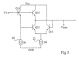
- a cell of the type of figure 3 is associated with each input voltage to be processed to achieve a circuit for supplying the lowest voltage or, in the embodiments described, the highest voltage of the input voltages. To create a supply circuit for the lowest voltage, it will suffice to make the cells of symmetrically by inverting the type of the transistors.
- the cell includes an NPN Q10 transistor receiving the voltage at its base V1 input associated with the cell.
- the transistor collector Q10 is connected to a high Vcc supply potential and its transmitter is connected to a Vmax line, common to all circuit cells, which provides the extremum voltage, the voltage maximum in this example.
- Voltage V1 is also supplied to the base of an NPN Q11 transistor connected in parallel by its base and its collector on transistor Q10.
- the transistor emitter Q11 is connected to GND ground by a current source 20 delivering a current I0.
- the emitter of transistor Q10 is connected to the collector an NPN transistor Q12 whose base receives the emitter voltage of transistor Q11 and whose emitter is connected to ground by a current source 22 delivering a current 2I0.
- a transistor NPN Q13 forms with the transistor Q12 a differential stage. This transistor Q13 has its emitter connected to the emitter of the transistor Q12, its base connected to the emitter of transistor Q10, and its collector connected to the voltage Vcc.
- transistor Q10 behaves in follower and the voltage Vmax is equal to the voltage V1 minus the base-emitter voltage Vbe0 of transistor Q10.
- the transistor Q11 also behaves as a follower and it appears on the base of transistor Q12 the voltage V1 minus the base-emitter voltage Vbe1 of transistor Q11. So the differential stage Q12, Q13 receives two almost equal voltages, which causes uniform distribution of current from source 22 in transistors Q12 and Q13. It follows that a current IO through transistor Q10, which is the same current as that passing through transistor Q11. So the base-emitter voltages transistors Q10 and Q11 are equal, which only confirm the steady state of stage Q12, Q13.
- the transistor Q12 of the differential stage receives on its base a voltage lower than the voltage of base Vmax of transistor Q13.
- the differential stage is unbalanced, and all the current from source 22 goes through the transistor Q13. So the current that the transistor can no longer conduct Q10 is not supplied by the Vmax line to the counterpart of the transistor Q10 from another cell.
- the differential stage Q12, Q13 behaves like a switch which prevents the supply of current (I0) to the common line Vmax as soon as transistor Q10 can no longer conduct this current.
Landscapes
- Physics & Mathematics (AREA)
- General Physics & Mathematics (AREA)
- Amplifiers (AREA)
- Electronic Switches (AREA)
Applications Claiming Priority (2)
| Application Number | Priority Date | Filing Date | Title |
|---|---|---|---|
| FR9415671A FR2728744B1 (fr) | 1994-12-21 | 1994-12-21 | Circuit de fourniture de tension extremum |
| FR9415671 | 1994-12-21 |
Publications (2)
| Publication Number | Publication Date |
|---|---|
| EP0718634A1 EP0718634A1 (fr) | 1996-06-26 |
| EP0718634B1 true EP0718634B1 (fr) | 2001-08-22 |
Family
ID=9470259
Family Applications (1)
| Application Number | Title | Priority Date | Filing Date |
|---|---|---|---|
| EP95410143A Expired - Lifetime EP0718634B1 (fr) | 1994-12-21 | 1995-12-18 | Circuit bipolaire de fourniture de tension extremum |
Country Status (5)
| Country | Link |
|---|---|
| US (1) | US5757209A (ja) |
| EP (1) | EP0718634B1 (ja) |
| JP (1) | JP2829361B2 (ja) |
| DE (1) | DE69522306D1 (ja) |
| FR (1) | FR2728744B1 (ja) |
Families Citing this family (2)
| Publication number | Priority date | Publication date | Assignee | Title |
|---|---|---|---|---|
| US6084439A (en) * | 1997-07-02 | 2000-07-04 | Cypress Semiconductor Corp. | Peak detector circuit with extended input voltage range |
| US6054874A (en) * | 1997-07-02 | 2000-04-25 | Cypress Semiconductor Corp. | Output driver circuit with switched current source |
Family Cites Families (13)
| Publication number | Priority date | Publication date | Assignee | Title |
|---|---|---|---|---|
| US3348072A (en) * | 1965-05-26 | 1967-10-17 | Ira R Marcus | Low-voltage wide-range comparator and rectifier using a plurality of emitter-follower circuits with the collector current of the conducting emitter-follower maintained constant |
| GB1241454A (en) * | 1968-12-06 | 1971-08-04 | English Electric Co Ltd | Maximum and minimum signal selectors |
| US3678513A (en) * | 1970-10-28 | 1972-07-18 | Gen Monitors | Peak selection circuit and apparatus utilizing same |
| JP2779411B2 (ja) * | 1985-03-01 | 1998-07-23 | キヤノン株式会社 | スイツチング装置 |
| JPS6234416A (ja) * | 1985-08-07 | 1987-02-14 | Victor Co Of Japan Ltd | 信号選択回路 |
| US4937670A (en) * | 1989-01-31 | 1990-06-26 | Rca Licensing Corporation | Peak detector with feedback |
| JPH03173289A (ja) * | 1989-12-01 | 1991-07-26 | Toshiba Corp | 最大値/最小値回路 |
| JPH04158687A (ja) * | 1990-10-23 | 1992-06-01 | Toshiba Corp | 最小値回路 |
| DE4115413C2 (de) * | 1991-05-10 | 1994-05-26 | Texas Instruments Deutschland | Schaltungsanordnung zur Erzeugung eines Schaltimpulses |
| JP2739800B2 (ja) * | 1992-08-04 | 1998-04-15 | 日本電気株式会社 | 半導体集積回路 |
| JPH0676090A (ja) * | 1992-08-26 | 1994-03-18 | Takayama:Kk | 最大値回路 |
| DE4237122C2 (de) * | 1992-11-03 | 1996-12-12 | Texas Instruments Deutschland | Schaltungsanordnung zur Überwachung des Drainstromes eines Metall-Oxid-Halbleiter-Feldeffekttransistors |
| US5469104A (en) * | 1994-03-28 | 1995-11-21 | Elantec, Inc. | Active folded cascode |
-
1994
- 1994-12-21 FR FR9415671A patent/FR2728744B1/fr not_active Expired - Fee Related
-
1995
- 1995-12-18 EP EP95410143A patent/EP0718634B1/fr not_active Expired - Lifetime
- 1995-12-18 DE DE69522306T patent/DE69522306D1/de not_active Expired - Lifetime
- 1995-12-18 US US08/573,898 patent/US5757209A/en not_active Expired - Lifetime
- 1995-12-20 JP JP7331749A patent/JP2829361B2/ja not_active Expired - Lifetime
Also Published As
| Publication number | Publication date |
|---|---|
| DE69522306D1 (de) | 2001-09-27 |
| US5757209A (en) | 1998-05-26 |
| FR2728744B1 (fr) | 1997-03-14 |
| FR2728744A1 (fr) | 1996-06-28 |
| JP2829361B2 (ja) | 1998-11-25 |
| JPH08321754A (ja) | 1996-12-03 |
| EP0718634A1 (fr) | 1996-06-26 |
Similar Documents
| Publication | Publication Date | Title |
|---|---|---|
| EP0731562B1 (fr) | Circuit logique à étage différentiel | |
| EP0838745B1 (fr) | Régulateur de tension à sélection automatique d'une tension d'alimentation la plus élevée | |
| EP0680140B1 (fr) | Amplificateur différentiel à réglage de mode commun | |
| EP0511707B1 (fr) | Amplificateur différentiel notamment du type à cascode | |
| EP0587509B1 (fr) | Circuit convertisseur tension/courant | |
| EP0845856B1 (fr) | Amplificateur à transconductance à dynamique élevée et faible bruit | |
| EP0913931B1 (fr) | Amplificateur à fort gain ayant une dynamique de sortie limitée | |
| EP0649079B1 (fr) | Circuit générateur de tension stabilisée du type bandgap | |
| FR2809834A1 (fr) | Source de courant a faible tension d'alimentation et a faible sensibilite en tension | |
| FR2825806A1 (fr) | Circuit de polarisation a point de fonctionnement stable en tension et en temperature | |
| EP0230693A1 (fr) | Etage amplificateur différentiel pour hautes fréquences et amplificateur muni d'un tel étage amplificateur différentiel | |
| EP0718634A1 (fr) | Circuit de fourniture de tension extremum | |
| EP0838746B1 (fr) | Régulateur de tension | |
| FR2728745A1 (fr) | Circuit de fourniture de tension extremum | |
| EP0722247B1 (fr) | Circuit de suppression et circuit d'accentuation | |
| EP0699359B1 (fr) | Circuit electronique, notamment resistance reglable, resistance negative, ou filtre ou analogue, commandes par un courant de polarisation | |
| EP0711034B1 (fr) | Dispositif de génération de fonctions de transfert définies par intervalles | |
| EP0353808B1 (fr) | Circuit de compensation de courant | |
| EP0479377B1 (fr) | Source de courant à rapport donné entre courant de sortie et d'entrée | |
| EP0722217B1 (fr) | Circuit de réglage du seuil de supression d'un signal | |
| EP0109106A1 (fr) | Circuit convertisseur de niveaux de signaux entre une logique de type saturée et une logique de type non saturée | |
| EP0700162A1 (fr) | Circuit logique à étages différentiels | |
| FR2801116A1 (fr) | Dispositif generateur de tension corrige a basse temperature | |
| EP0242304B1 (fr) | Amplificateur suiveur à grande vitesse | |
| FR2741212A1 (fr) | Dispositif de limitation du courant de sortie d'un amplificateur operationnel |
Legal Events
| Date | Code | Title | Description |
|---|---|---|---|
| PUAI | Public reference made under article 153(3) epc to a published international application that has entered the european phase |
Free format text: ORIGINAL CODE: 0009012 |
|
| AK | Designated contracting states |
Kind code of ref document: A1 Designated state(s): DE FR GB IT |
|
| 17P | Request for examination filed |
Effective date: 19961129 |
|
| RAP3 | Party data changed (applicant data changed or rights of an application transferred) |
Owner name: STMICROELECTRONICS S.A. |
|
| 17Q | First examination report despatched |
Effective date: 19991013 |
|
| RTI1 | Title (correction) |
Free format text: BIPOLAR CIRCUIT FOR GENERATING A VOLTAGE EXTREMUM |
|
| GRAG | Despatch of communication of intention to grant |
Free format text: ORIGINAL CODE: EPIDOS AGRA |
|
| GRAG | Despatch of communication of intention to grant |
Free format text: ORIGINAL CODE: EPIDOS AGRA |
|
| GRAH | Despatch of communication of intention to grant a patent |
Free format text: ORIGINAL CODE: EPIDOS IGRA |
|
| GRAH | Despatch of communication of intention to grant a patent |
Free format text: ORIGINAL CODE: EPIDOS IGRA |
|
| GRAA | (expected) grant |
Free format text: ORIGINAL CODE: 0009210 |
|
| AK | Designated contracting states |
Kind code of ref document: B1 Designated state(s): DE FR GB IT |
|
| PG25 | Lapsed in a contracting state [announced via postgrant information from national office to epo] |
Ref country code: IT Free format text: LAPSE BECAUSE OF FAILURE TO SUBMIT A TRANSLATION OF THE DESCRIPTION OR TO PAY THE FEE WITHIN THE PRESCRIBED TIME-LIMIT;WARNING: LAPSES OF ITALIAN PATENTS WITH EFFECTIVE DATE BEFORE 2007 MAY HAVE OCCURRED AT ANY TIME BEFORE 2007. THE CORRECT EFFECTIVE DATE MAY BE DIFFERENT FROM THE ONE RECORDED. Effective date: 20010822 Ref country code: GB Free format text: LAPSE BECAUSE OF FAILURE TO SUBMIT A TRANSLATION OF THE DESCRIPTION OR TO PAY THE FEE WITHIN THE PRESCRIBED TIME-LIMIT Effective date: 20010822 |
|
| REF | Corresponds to: |
Ref document number: 69522306 Country of ref document: DE Date of ref document: 20010927 |
|
| PG25 | Lapsed in a contracting state [announced via postgrant information from national office to epo] |
Ref country code: DE Free format text: LAPSE BECAUSE OF FAILURE TO SUBMIT A TRANSLATION OF THE DESCRIPTION OR TO PAY THE FEE WITHIN THE PRESCRIBED TIME-LIMIT Effective date: 20011123 |
|
| RAP2 | Party data changed (patent owner data changed or rights of a patent transferred) |
Owner name: STMICROELECTRONICS S.A. |
|
| GBV | Gb: ep patent (uk) treated as always having been void in accordance with gb section 77(7)/1977 [no translation filed] |
Effective date: 20010822 |
|
| PLBE | No opposition filed within time limit |
Free format text: ORIGINAL CODE: 0009261 |
|
| STAA | Information on the status of an ep patent application or granted ep patent |
Free format text: STATUS: NO OPPOSITION FILED WITHIN TIME LIMIT |
|
| 26N | No opposition filed | ||
| PG25 | Lapsed in a contracting state [announced via postgrant information from national office to epo] |
Ref country code: FR Free format text: LAPSE BECAUSE OF NON-PAYMENT OF DUE FEES Effective date: 20020830 |
|
| REG | Reference to a national code |
Ref country code: FR Ref legal event code: ST |