EP0709890B1 - Circuit de commande pour dispositifs électroniques à semi-conducteur avec au moins un transistor de puissance - Google Patents
Circuit de commande pour dispositifs électroniques à semi-conducteur avec au moins un transistor de puissance Download PDFInfo
- Publication number
- EP0709890B1 EP0709890B1 EP94830505A EP94830505A EP0709890B1 EP 0709890 B1 EP0709890 B1 EP 0709890B1 EP 94830505 A EP94830505 A EP 94830505A EP 94830505 A EP94830505 A EP 94830505A EP 0709890 B1 EP0709890 B1 EP 0709890B1
- Authority
- EP
- European Patent Office
- Prior art keywords
- type
- well
- transistor
- effect transistor
- channel field
- Prior art date
- Legal status (The legal status is an assumption and is not a legal conclusion. Google has not performed a legal analysis and makes no representation as to the accuracy of the status listed.)
- Expired - Lifetime
Links
- 239000004065 semiconductor Substances 0.000 title claims description 15
- 238000002955 isolation Methods 0.000 claims description 27
- 239000002019 doping agent Substances 0.000 claims description 25
- 230000005669 field effect Effects 0.000 claims description 13
- 238000002513 implantation Methods 0.000 claims description 13
- 238000009792 diffusion process Methods 0.000 claims description 10
- 239000000758 substrate Substances 0.000 claims description 10
- 238000000034 method Methods 0.000 claims description 9
- 230000003071 parasitic effect Effects 0.000 description 26
- 101001042415 Cratylia mollis Mannose/glucose-specific lectin Cramoll Proteins 0.000 description 4
- 102100029775 Eukaryotic translation initiation factor 1 Human genes 0.000 description 4
- 101001012787 Homo sapiens Eukaryotic translation initiation factor 1 Proteins 0.000 description 4
- 101000643378 Homo sapiens Serine racemase Proteins 0.000 description 4
- AIXMJTYHQHQJLU-UHFFFAOYSA-N chembl210858 Chemical compound O1C(CC(=O)OC)CC(C=2C=CC(O)=CC=2)=N1 AIXMJTYHQHQJLU-UHFFFAOYSA-N 0.000 description 4
- 230000015572 biosynthetic process Effects 0.000 description 3
- 210000000746 body region Anatomy 0.000 description 2
- 230000007423 decrease Effects 0.000 description 2
- 239000007943 implant Substances 0.000 description 2
- ZOXJGFHDIHLPTG-UHFFFAOYSA-N Boron Chemical compound [B] ZOXJGFHDIHLPTG-UHFFFAOYSA-N 0.000 description 1
- 229910052796 boron Inorganic materials 0.000 description 1
- 238000000151 deposition Methods 0.000 description 1
- 230000008021 deposition Effects 0.000 description 1
- 230000000694 effects Effects 0.000 description 1
- 230000010354 integration Effects 0.000 description 1
- 238000004519 manufacturing process Methods 0.000 description 1
- 238000001465 metallisation Methods 0.000 description 1
- 229910021420 polycrystalline silicon Inorganic materials 0.000 description 1
- 229920005591 polysilicon Polymers 0.000 description 1
- 229920006395 saturated elastomer Polymers 0.000 description 1
Images


Classifications
-
- H—ELECTRICITY
- H01—ELECTRIC ELEMENTS
- H01L—SEMICONDUCTOR DEVICES NOT COVERED BY CLASS H10
- H01L27/00—Devices consisting of a plurality of semiconductor or other solid-state components formed in or on a common substrate
- H01L27/02—Devices consisting of a plurality of semiconductor or other solid-state components formed in or on a common substrate including semiconductor components specially adapted for rectifying, oscillating, amplifying or switching and having potential barriers; including integrated passive circuit elements having potential barriers
- H01L27/04—Devices consisting of a plurality of semiconductor or other solid-state components formed in or on a common substrate including semiconductor components specially adapted for rectifying, oscillating, amplifying or switching and having potential barriers; including integrated passive circuit elements having potential barriers the substrate being a semiconductor body
- H01L27/08—Devices consisting of a plurality of semiconductor or other solid-state components formed in or on a common substrate including semiconductor components specially adapted for rectifying, oscillating, amplifying or switching and having potential barriers; including integrated passive circuit elements having potential barriers the substrate being a semiconductor body including only semiconductor components of a single kind
- H01L27/085—Devices consisting of a plurality of semiconductor or other solid-state components formed in or on a common substrate including semiconductor components specially adapted for rectifying, oscillating, amplifying or switching and having potential barriers; including integrated passive circuit elements having potential barriers the substrate being a semiconductor body including only semiconductor components of a single kind including field-effect components only
- H01L27/088—Devices consisting of a plurality of semiconductor or other solid-state components formed in or on a common substrate including semiconductor components specially adapted for rectifying, oscillating, amplifying or switching and having potential barriers; including integrated passive circuit elements having potential barriers the substrate being a semiconductor body including only semiconductor components of a single kind including field-effect components only the components being field-effect transistors with insulated gate
- H01L27/092—Devices consisting of a plurality of semiconductor or other solid-state components formed in or on a common substrate including semiconductor components specially adapted for rectifying, oscillating, amplifying or switching and having potential barriers; including integrated passive circuit elements having potential barriers the substrate being a semiconductor body including only semiconductor components of a single kind including field-effect components only the components being field-effect transistors with insulated gate complementary MIS field-effect transistors
- H01L27/0928—Devices consisting of a plurality of semiconductor or other solid-state components formed in or on a common substrate including semiconductor components specially adapted for rectifying, oscillating, amplifying or switching and having potential barriers; including integrated passive circuit elements having potential barriers the substrate being a semiconductor body including only semiconductor components of a single kind including field-effect components only the components being field-effect transistors with insulated gate complementary MIS field-effect transistors comprising both N- and P- wells in the substrate, e.g. twin-tub
-
- H—ELECTRICITY
- H01—ELECTRIC ELEMENTS
- H01L—SEMICONDUCTOR DEVICES NOT COVERED BY CLASS H10
- H01L27/00—Devices consisting of a plurality of semiconductor or other solid-state components formed in or on a common substrate
- H01L27/02—Devices consisting of a plurality of semiconductor or other solid-state components formed in or on a common substrate including semiconductor components specially adapted for rectifying, oscillating, amplifying or switching and having potential barriers; including integrated passive circuit elements having potential barriers
- H01L27/04—Devices consisting of a plurality of semiconductor or other solid-state components formed in or on a common substrate including semiconductor components specially adapted for rectifying, oscillating, amplifying or switching and having potential barriers; including integrated passive circuit elements having potential barriers the substrate being a semiconductor body
- H01L27/06—Devices consisting of a plurality of semiconductor or other solid-state components formed in or on a common substrate including semiconductor components specially adapted for rectifying, oscillating, amplifying or switching and having potential barriers; including integrated passive circuit elements having potential barriers the substrate being a semiconductor body including a plurality of individual components in a non-repetitive configuration
- H01L27/0611—Devices consisting of a plurality of semiconductor or other solid-state components formed in or on a common substrate including semiconductor components specially adapted for rectifying, oscillating, amplifying or switching and having potential barriers; including integrated passive circuit elements having potential barriers the substrate being a semiconductor body including a plurality of individual components in a non-repetitive configuration integrated circuits having a two-dimensional layout of components without a common active region
- H01L27/0617—Devices consisting of a plurality of semiconductor or other solid-state components formed in or on a common substrate including semiconductor components specially adapted for rectifying, oscillating, amplifying or switching and having potential barriers; including integrated passive circuit elements having potential barriers the substrate being a semiconductor body including a plurality of individual components in a non-repetitive configuration integrated circuits having a two-dimensional layout of components without a common active region comprising components of the field-effect type
- H01L27/0623—Devices consisting of a plurality of semiconductor or other solid-state components formed in or on a common substrate including semiconductor components specially adapted for rectifying, oscillating, amplifying or switching and having potential barriers; including integrated passive circuit elements having potential barriers the substrate being a semiconductor body including a plurality of individual components in a non-repetitive configuration integrated circuits having a two-dimensional layout of components without a common active region comprising components of the field-effect type in combination with bipolar transistors
Definitions
- This invention relates to a control circuit for semiconductor electronic devices which include at least one power transistor.
- the invention specifically concerns a control circuit for electronic power devices monolithically integrated on a semiconductor substrate which has been doped by a first dopant type and on which a first epitaxial layer doped by the same dopant type as the substrate has been grown, an isolation well doped by a second type of dopant being formed therein for at least a first transistor of the control circuit.
- the invention also relates to a semiconductor electronic device structure, in particular a field-effect transistor.
- the invention relates to a process for making the above control circuit and semiconductor device structure.
- At least one control circuit comprising low voltage operating transistors and at least one high voltage operating power transistor are integrated into many electronic devices.
- isolation structure is used for the control circuit, and its related transistors are integrated in a single well, known as the isolation well, such as the one shown at 3' in Figure 1.
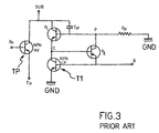
- Figure 1 shows schematically a semiconductor IC device which has been integrated monolithically in accordance with prior art methods and comprises a control circuit C' and a power transistor TP of the bipolar NPN HV type.
- the IC device has a pair of isolation terminals ISO1 and ISO2.
- control circuit C' of Figure 1 has been depicted as having two bipolar components only, namely a transistor T1 of the NPN LV type and a transistor T2 of the PNP LV type.
- control transistors T1 and T2 are accommodated in a single isolation well 3' formed within an epitaxial layer 2' of the N- type grown on a substrate 1' of the N+ type.
- the isolation well 3' is virtually a necessity with semiconductor devices of this kind, but involves the appearance of certain parasitic transistors which impair the proper operation of the control circuit.
- each of the control transistors T1 and T2 involves the presence, in the isolation well 3', of respective buried layers 4' and 4'' having a dopant type which is the opposite from that of the well 3'. These buried layers 4' and 4'' are responsible for the appearance of several parasitic transistors.
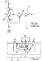
- FIG. 1 shows, drawn to an enlarged scale, a portion of Figure 1 where just the transistor T1 and the layer 4' are provided.
- An equivalent electric circuit of the structure of Figure 2 is shown in Figure 3.
- the base-emitter junction of the parasitic transistor P2' is forward biased and its collector, which is coincident with a contact ISO1 of the isolation well 3', is at a ground reference potential GND.
- the transistor P2' will be in the active zone and will inject current into an isolation area 9' which is associated with the contact ISO1 through a resistance Rp being the intrinsic resistance of the well 3'.
- This occurrence may result from the presence of ramp voltages applied to the substrate 1', which can charge a parasitic capacitance Cp, present between the substrate 1' and the well 3', and produce a current flow which can turn on the parasitic transistor P1'.
- Figure 4A is an enlarged view of the structure of the transistor T2, while Figure 4B shows an equivalent electric circuit of Figure 4A.
- the presence of the parasitic transistor P1' is less critical to the control transistor T2 than to the previous transistor T1 because the emitter of the transistor P1' is at a higher voltage than the ground voltage, and to turn on the transistor P1', its base-emitter junction must be brought up to an even higher value.
- the current which is forced to flow through the resistance Rp is, therefore, a larger one if compared to the control transistor T1.
- a first known technical solution to meet such requirements consists of using an isolation well 3' obtained by epitaxial growth rather than implantation followed by dopant diffusion.
- the base of the parasitic transistor P1' is more strongly doped, and this brings down the transistor gain.
- the technical problem underlying this invention is to provide a control circuit adapted for monolithic integration, with at least one driven power transistor, and having such structural and functional features as to afford a drastic reduction in the parasitic components that appear in previously known solutions in the art.
- the solutive idea on which the invention stands is one of providing the control circuit with at least one N-channel MOS transistor placed in a well in direct contact with the isolation well.
- control circuit C is a control circuit embodying this invention.
- bipolar power transistor TP which is understood to have been conventionally integrated monolithically together with the control circuit C to be driven by the latter.
- control circuit C comprising just two transistors M1 and M2 will be considered for discussion.
- such transistors are field-effect, in particular MOS, transistors of the N-channel and the P-channel type, respectively.
- a first growth step is carried out to provide a first epitaxial layer 2 which has the same first dopant type.
- This first epitaxial layer 2 contains N dopant to a lower concentration than the substrate 1.
- a step of implantation and diffusion of a second dopant type e.g. a P type, is carried out on the epitaxial layer 2, thereby to form an isolation well 3 in the epitaxial layer 2.
- a second dopant type e.g. a P type
- the isolation well 3 is then subjected to a third implantation and diffusion step at a high concentration of the first N+ dopant type to form a layer 4.
- the last-mentioned layer 4 will be termed "buried" hereinafter for reasons to be explained.
- the buried layer 4 is used to form a single MOS transistor, the P-channel transistor M2.
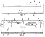
- a fourth growth step is carried out to grow a second epitaxial layer 5 having a low concentration of the first type of N dopant, which low concentration is comparable to that of the first epitaxial layer 2.
- a fifth implantation step of the second type of P dopant will result in a second P-well 6 being formed within the second epitaxial layer 5.
- a sixth implantation step of the first type of N dopant will provide a third N-well 7 over the buried layer 4. This implant will also affect the epitaxial layer surrounding the P-well 6, raising its dopant concentration.
- a subsequent thermal diffusion step will settle the dopings of the wells 6 and 7.
- This implant will essentially define three discrete connect channels extending from the semiconductor surface down the isolation well 3.
- These connect channels 9 bound the third N-well 7 and a fourth N-well 8 accommodating the P-well 6 over the isolation well 3.
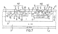
- the circuit structure will show up as in Figure 6, with an isolation well 3 accommodating and enclosing two N-wells 7, 8, one being formed over the buried layer 4 and the other housing a P-well 6.
- the first MOS transistor M1 of the N-channel type and the second MOS transistor M2 of the P-channel type are respectively formed in the wells 6 and 7.
- these transistors M1 and M2 have been shown in their final structure condition, separately and to an enlarged scale, in Figures 8 and 9.
- An implantation and associated diffusion step of the second type of P dopant into the well 6 allows definition of deep body regions 12, 12' as well as the regions 13, 13' in the well 7.
- a layer 17 of polysilicon is deposited onto the semiconductor surface and suitably doped to form the gates G1 and G2 of the MOS transistors M1 and M2.
- This deposition step is followed by an implantation and diffusion step of dopant of the second P type into the third well 7 to form the drain and source active areas 14 and 14' of the P-channel transistor M2.
- the fabricating process is completed by a step of definition and metallization of the drain contact areas D1, D2 and source contact areas S1, S2.
- the resultant device is as shown in Figure 7.
- the transistor M1 has no buried layer of dopant of the first N type, as was instead the case with prior art bipolar transistors. It will be recalled, in fact, that the NPN transistor T1 of Figures 1 and 2 has its collector defined by the buried layer 4', which provides a near-vertical, substantially U-like current flow pattern.
- a first parasitic transistor P1 By eliminating the buried layer of the first dopant type, a first parasitic transistor P1, whose emitter is indeed formed by that layer, can also be suppressed.
- any second parasitic transistor P2 such as affects, by contrast, all prior embodiments.
- the source S1 of the transistor M1 is connected to the ground reference potential GND, and so is, therefore, the deep body region 12' to which that source S1 is connected.
- the emitter and base of the parasitic transistor P2 are shorted together and the transistor P2 cannot be turned on.
- the buried layer 4 of the first type of N+ dopant is, however, still present in the well 7 where the P-channel transistor M2 is formed, which prevents shorting of the source S2 to the drain D2 of that transistor M2. Accordingly, the formation of the control transistor M2 will imply the presence of a parasitic transistor P1 due to the buried layer 4 provided.
- the P + -N junction between the region 13 and the well 7 of the control transistor M2 will at all times be reverse biased to prevent said parasitic transistor P1 from becoming turned on.
- the source contact S2 stops operation of a further parasitic transistor P3 by shorting its base to its emitter, coincident with the regions 11 and 13'.
- control circuit C of this invention does remove the problems brought about by the appearance of parasitic elements, thereby overcoming the drawbacks of similar prior art circuits.
Landscapes
- Engineering & Computer Science (AREA)
- Power Engineering (AREA)
- Physics & Mathematics (AREA)
- Condensed Matter Physics & Semiconductors (AREA)
- General Physics & Mathematics (AREA)
- Computer Hardware Design (AREA)
- Microelectronics & Electronic Packaging (AREA)
- Metal-Oxide And Bipolar Metal-Oxide Semiconductor Integrated Circuits (AREA)
- Element Separation (AREA)
Claims (6)
- Un circuit de puissance intégré comprenant :un transistor de puissance (TP) intégré de façon monolithique dans un substrat semi-conducteur de type N (2) ;un caisson d'isolation de type P à motif (3) dans ledit substrat (2) ;un transistor à effet de champ à canal N (M1) se trouvant à l'intérieur d'un second caisson de type P (6) formé dans un premier caisson de type N (8) formé dans ledit caisson d'isolation de type P (3) ;un transistor à effet de champ à canal P (M2) se trouvant à l'intérieur d'un second caisson de type N (7) formé dans ledit caisson d'isolation de type P (3) ;une couche enterrée de type N (4) formée dans ledit caisson d'isolation de type P (3) et à la base dudit second caisson de type N (7), et ayant une concentration de dopage plus forte que celle dudit second caisson de type N (7).
- Un circuit de puissance intégré selon la revendication 1, dans lequel ledit transistor à effet de champ à canal N (M1) comprend en outre une région de diffusion de contact de type P (12, 12') limitant le bord latéral dudit second caisson de type P (6) et étant connectée à la source dudit transistor à effet de champ à canal N (M1).
- Un circuit de puissance intégré selon la revendication 1, dans lequel ledit transistor à effet de champ à canal P (M2) comprend en outre des régions de diffusion de contact de type P (13, 13') limitant respectivement les régions de source et de drain dudit transistor à canal P (M2) à l'intérieur dudit second caisson du type N (7).
- Un circuit de puissance intégré selon la revendication 1 ou 2 ou 3, dans lequel ledit transistor à effet de champ à canal N (M1) et ledit transistor à effet de champ à canal P (M2) sont des transistors MOS.
- Un procédé de fabrication d'un circuit de puissance intégré destiné à des dispositifs électroniques semi-conducteurs intégrés de façon monolithique avec au moins un composant de puissance, étant d'un type qui comprend une première étape de croissance d'une première couche épitaxiale (2) de type N sur un substrat semi-conducteur de type N+ (1), une première étape d'implantation d'un dopant de type P pour définir un caisson d'isolation de type P (3), une seconde étape d'implantation pour définir une couche enterrée de type N+ (4) dans une partie de la surface dudit caisson d'isolation de type P (3), et une seconde étape de croissance d'une seconde couche épitaxiale de type N (5) sur la première couche épitaxiale (2), une autre étape d'implantation mise en oeuvre en utilisant un dopant de type P pour former trois canaux discrets de type P+ (9) s'étendant à partir de la surface de ladite seconde couche épitaxiale de type N (5) jusqu'audit caisson d'isolation de type P (3), afin de définir un premier caisson de type N (8) dans ladite seconde couche épitaxiale (5), et un second caisson de type N (7) dans ladite seconde couche épitaxiale (5) sur ladite couche enterrée de type N (4), et séparé dudit premier caisson de type N (8) par l'un desdits trois canaux discrets de type P+ (9), et ensuite une autre étape d'implantation pour définir un second caisson de type P (6) formé dans ledit premier caisson de type N (8), constituant un transistor à effet de champ à canal N (M1) dans ledit second caisson de type P (3), et constituant un second transistor à effet de champ à canal P (M2) dans ledit second caisson de type N (7) formé sur ladite couche enterrée de type N (4).
- Un procédé selon la revendication 5, dans lequel ledit transistor à effet de champ à canal N (M1) et ledit transistor à effet de champ à canal P (M2) sont des transistor MOS.
Priority Applications (5)
| Application Number | Priority Date | Filing Date | Title |
|---|---|---|---|
| DE69420565T DE69420565T2 (de) | 1994-10-27 | 1994-10-27 | Treiberschaltung für elektronische Halbleiterbauelemente mit wenigstens einem Leistungstransistor |
| EP94830505A EP0709890B1 (fr) | 1994-10-27 | 1994-10-27 | Circuit de commande pour dispositifs électroniques à semi-conducteur avec au moins un transistor de puissance |
| JP7280502A JPH08274183A (ja) | 1994-10-27 | 1995-10-27 | 半導体装置、制御回路およびその製造方法 |
| US08/549,599 US5708290A (en) | 1994-10-27 | 1995-10-27 | Driving circuit for electronic semiconductor devices including at least a power transistor |
| US08/929,349 US6033947A (en) | 1994-10-27 | 1997-08-25 | Driving circuit for electronic semiconductor devices including at least a power transistor |
Applications Claiming Priority (1)
| Application Number | Priority Date | Filing Date | Title |
|---|---|---|---|
| EP94830505A EP0709890B1 (fr) | 1994-10-27 | 1994-10-27 | Circuit de commande pour dispositifs électroniques à semi-conducteur avec au moins un transistor de puissance |
Publications (2)
| Publication Number | Publication Date |
|---|---|
| EP0709890A1 EP0709890A1 (fr) | 1996-05-01 |
| EP0709890B1 true EP0709890B1 (fr) | 1999-09-08 |
Family
ID=8218558
Family Applications (1)
| Application Number | Title | Priority Date | Filing Date |
|---|---|---|---|
| EP94830505A Expired - Lifetime EP0709890B1 (fr) | 1994-10-27 | 1994-10-27 | Circuit de commande pour dispositifs électroniques à semi-conducteur avec au moins un transistor de puissance |
Country Status (4)
| Country | Link |
|---|---|
| US (2) | US5708290A (fr) |
| EP (1) | EP0709890B1 (fr) |
| JP (1) | JPH08274183A (fr) |
| DE (1) | DE69420565T2 (fr) |
Families Citing this family (17)
| Publication number | Priority date | Publication date | Assignee | Title |
|---|---|---|---|---|
| US5896313A (en) * | 1997-06-02 | 1999-04-20 | Micron Technology, Inc. | Vertical bipolar SRAM cell, array and system, and a method of making the cell and the array |
| DE19752848C2 (de) * | 1997-11-28 | 2003-12-24 | Infineon Technologies Ag | Elektrisch entkoppelter Feldeffekt-Transistor in Dreifach-Wanne und Verwendung desselben |
| IT1298516B1 (it) * | 1998-01-30 | 2000-01-12 | Sgs Thomson Microelectronics | Dispositivo elettronico di potenza integrato su un materiale semiconduttore e relativo processo di fabricazione |
| US6495423B1 (en) | 1999-08-26 | 2002-12-17 | Stmicroelectronics S.R.L. | Electronic power device monolithically integrated on a semiconductor and comprising edge protection structures having a limited planar dimension |
| US6451655B1 (en) | 1999-08-26 | 2002-09-17 | Stmicroelectronics S.R.L. | Electronic power device monolithically integrated on a semiconductor and comprising a first power region and at least a second region as well as an isolation structure of limited planar dimension |
| US6245609B1 (en) * | 1999-09-27 | 2001-06-12 | Taiwan Semiconductor Manufacturing Company | High voltage transistor using P+ buried layer |
| JP2002324846A (ja) * | 2001-04-25 | 2002-11-08 | Sanken Electric Co Ltd | 半導体装置及びその製造方法 |
| JP2003258119A (ja) * | 2002-03-07 | 2003-09-12 | Seiko Epson Corp | 半導体装置の製造方法 |
| US6661042B2 (en) * | 2002-03-11 | 2003-12-09 | Monolithic System Technology, Inc. | One-transistor floating-body DRAM cell in bulk CMOS process with electrically isolated charge storage region |
| US6686624B2 (en) | 2002-03-11 | 2004-02-03 | Monolithic System Technology, Inc. | Vertical one-transistor floating-body DRAM cell in bulk CMOS process with electrically isolated charge storage region |
| US6946720B2 (en) * | 2003-02-13 | 2005-09-20 | Intersil Americas Inc. | Bipolar transistor for an integrated circuit having variable value emitter ballast resistors |
| JP2006013450A (ja) * | 2004-05-27 | 2006-01-12 | Renesas Technology Corp | 半導体装置およびその製造方法 |
| JP4890838B2 (ja) * | 2005-11-17 | 2012-03-07 | ルネサスエレクトロニクス株式会社 | 半導体集積回路のレイアウト設計方法、及びレイアウト設計ツール |
| JP2008042013A (ja) * | 2006-08-08 | 2008-02-21 | Sanyo Electric Co Ltd | 半導体装置の製造方法 |
| JP5119626B2 (ja) * | 2006-08-18 | 2013-01-16 | 富士通セミコンダクター株式会社 | 電気ヒューズ回路 |
| US9029750B1 (en) * | 2011-08-02 | 2015-05-12 | Northrop Grumman Systems Corporation | CMOS and CCD sensor R/O with high gain and no kTC noise |
| CN112289787B (zh) * | 2020-09-17 | 2024-01-26 | 南京通华芯微电子有限公司 | 一种具有多种控制功能的mos器件 |
Family Cites Families (7)
| Publication number | Priority date | Publication date | Assignee | Title |
|---|---|---|---|---|
| JPH0618255B2 (ja) * | 1984-04-04 | 1994-03-09 | 株式会社東芝 | 半導体装置 |
| JPS63198367A (ja) * | 1987-02-13 | 1988-08-17 | Toshiba Corp | 半導体装置 |
| IT1221587B (it) * | 1987-09-07 | 1990-07-12 | S G S Microelettronics Spa | Procedimento di fabbricazione di un dispositivo integrato monolitico a semiconduttore avente strati epitas siali a bassa concentrazione di impurita' |
| US5512774A (en) * | 1988-02-08 | 1996-04-30 | Kabushiki Kaisha Toshiba | Dielectrically isolated substrate and semiconductor device using the same |
| IT1228900B (it) * | 1989-02-27 | 1991-07-09 | Sgs Thomson Microelectronics | Struttura integrata monolitica per sistema di pilotaggio a due stadi con componente circuitale traslatore di livello del segnale di pilotaggio per transistori di potenza. |
| JPH07109861B2 (ja) * | 1990-01-19 | 1995-11-22 | 株式会社東芝 | 電荷転送デバイスを含む半導体装置およびその製造方法 |
| JP3216206B2 (ja) * | 1992-03-30 | 2001-10-09 | 株式会社デンソー | 半導体装置及びその製造方法 |
-
1994
- 1994-10-27 EP EP94830505A patent/EP0709890B1/fr not_active Expired - Lifetime
- 1994-10-27 DE DE69420565T patent/DE69420565T2/de not_active Expired - Fee Related
-
1995
- 1995-10-27 JP JP7280502A patent/JPH08274183A/ja active Pending
- 1995-10-27 US US08/549,599 patent/US5708290A/en not_active Expired - Lifetime
-
1997
- 1997-08-25 US US08/929,349 patent/US6033947A/en not_active Expired - Lifetime
Also Published As
| Publication number | Publication date |
|---|---|
| DE69420565T2 (de) | 2000-03-30 |
| EP0709890A1 (fr) | 1996-05-01 |
| US5708290A (en) | 1998-01-13 |
| JPH08274183A (ja) | 1996-10-18 |
| US6033947A (en) | 2000-03-07 |
| DE69420565D1 (de) | 1999-10-14 |
Similar Documents
| Publication | Publication Date | Title |
|---|---|---|
| EP0709890B1 (fr) | Circuit de commande pour dispositifs électroniques à semi-conducteur avec au moins un transistor de puissance | |
| US5034337A (en) | Method of making an integrated circuit that combines multi-epitaxial power transistors with logic/analog devices | |
| US4862233A (en) | Integrated circuit device having vertical MOS provided with Zener diode | |
| US6365447B1 (en) | High-voltage complementary bipolar and BiCMOS technology using double expitaxial growth | |
| US7718481B2 (en) | Semiconductor structure and method of manufacture | |
| US5665994A (en) | Integrated device with a bipolar transistor and a MOSFET transistor in an emitter switching configuration | |
| EP0683521B1 (fr) | Circuit intégré de puissance ("PIC") et son procédé de fabrication | |
| US7145206B2 (en) | MOS field effect transistor with reduced parasitic substrate conduction | |
| US4939099A (en) | Process for fabricating isolated vertical bipolar and JFET transistors | |
| US6249031B1 (en) | High gain lateral PNP and NPN bipolar transistor and process compatible with CMOS for making BiCMOS circuits | |
| US4914051A (en) | Method for making a vertical power DMOS transistor with small signal bipolar transistors | |
| US5132235A (en) | Method for fabricating a high voltage MOS transistor | |
| US5256582A (en) | Method of forming complementary bipolar and MOS transistor having power and logic structures on the same integrated circuit substrate | |
| JPH06151723A (ja) | モノリシック半導体素子のバイポーラトランジスタ構造、及び前記モノリシック半導体素子の製造方法 | |
| EP0746038B1 (fr) | Transistor PNP vertical isolé et sa méthode de fabrication | |
| US5556792A (en) | Process for manufacturing a power integrated circuit ("PIC") structure with a vertical IGBT | |
| US5070382A (en) | Semiconductor structure for high power integrated circuits | |
| US5181095A (en) | Complementary bipolar and MOS transistor having power and logic structures on the same integrated circuit substrate | |
| US6831346B1 (en) | Buried layer substrate isolation in integrated circuits | |
| US4969823A (en) | Integrated circuit with complementary junction-isolated bipolar transistors and method of making same | |
| US20040053439A1 (en) | Method for producing low-resistance ohmic contacts between substrates and wells in CMOS integrated circuits | |
| US6011283A (en) | Pillar emitter for BiCMOS devices | |
| US5065214A (en) | Integrated circuit with complementary junction-isolated bipolar transistors | |
| US6501152B1 (en) | Advanced lateral PNP by implant negation | |
| EP0348626B1 (fr) | Procédé pour l'intégration de transistors isolés bipolaires verticaux et JFET et circuit intégré correspondant |
Legal Events
| Date | Code | Title | Description |
|---|---|---|---|
| PUAI | Public reference made under article 153(3) epc to a published international application that has entered the european phase |
Free format text: ORIGINAL CODE: 0009012 |
|
| AK | Designated contracting states |
Kind code of ref document: A1 Designated state(s): DE FR GB IT |
|
| 17P | Request for examination filed |
Effective date: 19961021 |
|
| 17Q | First examination report despatched |
Effective date: 19961216 |
|
| GRAG | Despatch of communication of intention to grant |
Free format text: ORIGINAL CODE: EPIDOS AGRA |
|
| GRAG | Despatch of communication of intention to grant |
Free format text: ORIGINAL CODE: EPIDOS AGRA |
|
| GRAH | Despatch of communication of intention to grant a patent |
Free format text: ORIGINAL CODE: EPIDOS IGRA |
|
| GRAG | Despatch of communication of intention to grant |
Free format text: ORIGINAL CODE: EPIDOS AGRA |
|
| GRAH | Despatch of communication of intention to grant a patent |
Free format text: ORIGINAL CODE: EPIDOS IGRA |
|
| GRAH | Despatch of communication of intention to grant a patent |
Free format text: ORIGINAL CODE: EPIDOS IGRA |
|
| GRAA | (expected) grant |
Free format text: ORIGINAL CODE: 0009210 |
|
| AK | Designated contracting states |
Kind code of ref document: B1 Designated state(s): DE FR GB IT |
|
| ITF | It: translation for a ep patent filed |
Owner name: BOTTI & FERRARI S.R.L. |
|
| REF | Corresponds to: |
Ref document number: 69420565 Country of ref document: DE Date of ref document: 19991014 |
|
| ET | Fr: translation filed | ||
| PLBE | No opposition filed within time limit |
Free format text: ORIGINAL CODE: 0009261 |
|
| STAA | Information on the status of an ep patent application or granted ep patent |
Free format text: STATUS: NO OPPOSITION FILED WITHIN TIME LIMIT |
|
| 26N | No opposition filed | ||
| REG | Reference to a national code |
Ref country code: GB Ref legal event code: IF02 |
|
| PGFP | Annual fee paid to national office [announced via postgrant information from national office to epo] |
Ref country code: DE Payment date: 20030930 Year of fee payment: 10 |
|
| PG25 | Lapsed in a contracting state [announced via postgrant information from national office to epo] |
Ref country code: DE Free format text: LAPSE BECAUSE OF NON-PAYMENT OF DUE FEES Effective date: 20050503 |
|
| PG25 | Lapsed in a contracting state [announced via postgrant information from national office to epo] |
Ref country code: IT Free format text: LAPSE BECAUSE OF NON-PAYMENT OF DUE FEES;WARNING: LAPSES OF ITALIAN PATENTS WITH EFFECTIVE DATE BEFORE 2007 MAY HAVE OCCURRED AT ANY TIME BEFORE 2007. THE CORRECT EFFECTIVE DATE MAY BE DIFFERENT FROM THE ONE RECORDED. Effective date: 20051027 |
|
| PGFP | Annual fee paid to national office [announced via postgrant information from national office to epo] |
Ref country code: GB Payment date: 20060327 Year of fee payment: 12 |
|
| PGFP | Annual fee paid to national office [announced via postgrant information from national office to epo] |
Ref country code: FR Payment date: 20060329 Year of fee payment: 12 |
|
| GBPC | Gb: european patent ceased through non-payment of renewal fee |
Effective date: 20061027 |
|
| REG | Reference to a national code |
Ref country code: FR Ref legal event code: ST Effective date: 20070629 |
|
| PG25 | Lapsed in a contracting state [announced via postgrant information from national office to epo] |
Ref country code: GB Free format text: LAPSE BECAUSE OF NON-PAYMENT OF DUE FEES Effective date: 20061027 |
|
| PG25 | Lapsed in a contracting state [announced via postgrant information from national office to epo] |
Ref country code: FR Free format text: LAPSE BECAUSE OF NON-PAYMENT OF DUE FEES Effective date: 20061031 |