EP0704731B1 - Module optique à semi-conducteur et procédé pour sa fabrication - Google Patents
Module optique à semi-conducteur et procédé pour sa fabrication Download PDFInfo
- Publication number
- EP0704731B1 EP0704731B1 EP95306729A EP95306729A EP0704731B1 EP 0704731 B1 EP0704731 B1 EP 0704731B1 EP 95306729 A EP95306729 A EP 95306729A EP 95306729 A EP95306729 A EP 95306729A EP 0704731 B1 EP0704731 B1 EP 0704731B1
- Authority
- EP
- European Patent Office
- Prior art keywords
- substrate
- optical
- optical semiconductor
- airtight sealing
- semiconductor module
- Prior art date
- Legal status (The legal status is an assumption and is not a legal conclusion. Google has not performed a legal analysis and makes no representation as to the accuracy of the status listed.)
- Expired - Lifetime
Links
Images


Classifications
-
- G—PHYSICS
- G02—OPTICS
- G02B—OPTICAL ELEMENTS, SYSTEMS OR APPARATUS
- G02B6/00—Light guides; Structural details of arrangements comprising light guides and other optical elements, e.g. couplings
- G02B6/24—Coupling light guides
- G02B6/42—Coupling light guides with opto-electronic elements
- G02B6/4201—Packages, e.g. shape, construction, internal or external details
- G02B6/4204—Packages, e.g. shape, construction, internal or external details the coupling comprising intermediate optical elements, e.g. lenses, holograms
- G02B6/421—Packages, e.g. shape, construction, internal or external details the coupling comprising intermediate optical elements, e.g. lenses, holograms the intermediate optical component consisting of a short length of fibre, e.g. fibre stub
-
- G—PHYSICS
- G02—OPTICS
- G02B—OPTICAL ELEMENTS, SYSTEMS OR APPARATUS
- G02B6/00—Light guides; Structural details of arrangements comprising light guides and other optical elements, e.g. couplings
- G02B6/24—Coupling light guides
- G02B6/42—Coupling light guides with opto-electronic elements
- G02B6/4201—Packages, e.g. shape, construction, internal or external details
- G02B6/4202—Packages, e.g. shape, construction, internal or external details for coupling an active element with fibres without intermediate optical elements, e.g. fibres with plane ends, fibres with shaped ends, bundles
-
- G—PHYSICS
- G02—OPTICS
- G02B—OPTICAL ELEMENTS, SYSTEMS OR APPARATUS
- G02B6/00—Light guides; Structural details of arrangements comprising light guides and other optical elements, e.g. couplings
- G02B6/24—Coupling light guides
- G02B6/42—Coupling light guides with opto-electronic elements
- G02B6/4201—Packages, e.g. shape, construction, internal or external details
- G02B6/4248—Feed-through connections for the hermetical passage of fibres through a package wall
-
- G—PHYSICS
- G02—OPTICS
- G02B—OPTICAL ELEMENTS, SYSTEMS OR APPARATUS
- G02B6/00—Light guides; Structural details of arrangements comprising light guides and other optical elements, e.g. couplings
- G02B6/24—Coupling light guides
- G02B6/42—Coupling light guides with opto-electronic elements
- G02B6/4201—Packages, e.g. shape, construction, internal or external details
- G02B6/4251—Sealed packages
- G02B6/4253—Sealed packages by embedding housing components in an adhesive or a polymer material
-
- G—PHYSICS
- G02—OPTICS
- G02B—OPTICAL ELEMENTS, SYSTEMS OR APPARATUS
- G02B6/00—Light guides; Structural details of arrangements comprising light guides and other optical elements, e.g. couplings
- G02B6/24—Coupling light guides
- G02B6/42—Coupling light guides with opto-electronic elements
- G02B6/4201—Packages, e.g. shape, construction, internal or external details
- G02B6/4255—Moulded or casted packages
-
- G—PHYSICS
- G02—OPTICS
- G02B—OPTICAL ELEMENTS, SYSTEMS OR APPARATUS
- G02B6/00—Light guides; Structural details of arrangements comprising light guides and other optical elements, e.g. couplings
- G02B6/24—Coupling light guides
- G02B6/42—Coupling light guides with opto-electronic elements
- G02B6/4201—Packages, e.g. shape, construction, internal or external details
- G02B6/4256—Details of housings
- G02B6/4257—Details of housings having a supporting carrier or a mounting substrate or a mounting plate
-
- G—PHYSICS
- G02—OPTICS
- G02B—OPTICAL ELEMENTS, SYSTEMS OR APPARATUS
- G02B6/00—Light guides; Structural details of arrangements comprising light guides and other optical elements, e.g. couplings
- G02B6/24—Coupling light guides
- G02B6/42—Coupling light guides with opto-electronic elements
- G02B6/4201—Packages, e.g. shape, construction, internal or external details
- G02B6/4266—Thermal aspects, temperature control or temperature monitoring
- G02B6/4267—Reduction of thermal stress, e.g. by selecting thermal coefficient of materials
-
- G—PHYSICS
- G02—OPTICS
- G02B—OPTICAL ELEMENTS, SYSTEMS OR APPARATUS
- G02B6/00—Light guides; Structural details of arrangements comprising light guides and other optical elements, e.g. couplings
- G02B6/24—Coupling light guides
- G02B6/42—Coupling light guides with opto-electronic elements
- G02B6/4201—Packages, e.g. shape, construction, internal or external details
- G02B6/4266—Thermal aspects, temperature control or temperature monitoring
- G02B6/4268—Cooling
-
- G—PHYSICS
- G02—OPTICS
- G02B—OPTICAL ELEMENTS, SYSTEMS OR APPARATUS
- G02B6/00—Light guides; Structural details of arrangements comprising light guides and other optical elements, e.g. couplings
- G02B6/24—Coupling light guides
- G02B6/42—Coupling light guides with opto-electronic elements
- G02B6/4201—Packages, e.g. shape, construction, internal or external details
- G02B6/4219—Mechanical fixtures for holding or positioning the elements relative to each other in the couplings; Alignment methods for the elements, e.g. measuring or observing methods especially used therefor
- G02B6/4228—Passive alignment, i.e. without a detection of the degree of coupling or the position of the elements
- G02B6/423—Passive alignment, i.e. without a detection of the degree of coupling or the position of the elements using guiding surfaces for the alignment
-
- G—PHYSICS
- G02—OPTICS
- G02B—OPTICAL ELEMENTS, SYSTEMS OR APPARATUS
- G02B6/00—Light guides; Structural details of arrangements comprising light guides and other optical elements, e.g. couplings
- G02B6/24—Coupling light guides
- G02B6/42—Coupling light guides with opto-electronic elements
- G02B6/4201—Packages, e.g. shape, construction, internal or external details
- G02B6/4219—Mechanical fixtures for holding or positioning the elements relative to each other in the couplings; Alignment methods for the elements, e.g. measuring or observing methods especially used therefor
- G02B6/4236—Fixing or mounting methods of the aligned elements
- G02B6/4238—Soldering
-
- H—ELECTRICITY
- H01—ELECTRIC ELEMENTS
- H01L—SEMICONDUCTOR DEVICES NOT COVERED BY CLASS H10
- H01L2224/00—Indexing scheme for arrangements for connecting or disconnecting semiconductor or solid-state bodies and methods related thereto as covered by H01L24/00
- H01L2224/01—Means for bonding being attached to, or being formed on, the surface to be connected, e.g. chip-to-package, die-attach, "first-level" interconnects; Manufacturing methods related thereto
- H01L2224/26—Layer connectors, e.g. plate connectors, solder or adhesive layers; Manufacturing methods related thereto
- H01L2224/31—Structure, shape, material or disposition of the layer connectors after the connecting process
- H01L2224/32—Structure, shape, material or disposition of the layer connectors after the connecting process of an individual layer connector
- H01L2224/321—Disposition
- H01L2224/32151—Disposition the layer connector connecting between a semiconductor or solid-state body and an item not being a semiconductor or solid-state body, e.g. chip-to-substrate, chip-to-passive
- H01L2224/32221—Disposition the layer connector connecting between a semiconductor or solid-state body and an item not being a semiconductor or solid-state body, e.g. chip-to-substrate, chip-to-passive the body and the item being stacked
- H01L2224/32225—Disposition the layer connector connecting between a semiconductor or solid-state body and an item not being a semiconductor or solid-state body, e.g. chip-to-substrate, chip-to-passive the body and the item being stacked the item being non-metallic, e.g. insulating substrate with or without metallisation
-
- H—ELECTRICITY
- H01—ELECTRIC ELEMENTS
- H01L—SEMICONDUCTOR DEVICES NOT COVERED BY CLASS H10
- H01L2224/00—Indexing scheme for arrangements for connecting or disconnecting semiconductor or solid-state bodies and methods related thereto as covered by H01L24/00
- H01L2224/01—Means for bonding being attached to, or being formed on, the surface to be connected, e.g. chip-to-package, die-attach, "first-level" interconnects; Manufacturing methods related thereto
- H01L2224/42—Wire connectors; Manufacturing methods related thereto
- H01L2224/47—Structure, shape, material or disposition of the wire connectors after the connecting process
- H01L2224/48—Structure, shape, material or disposition of the wire connectors after the connecting process of an individual wire connector
- H01L2224/4805—Shape
- H01L2224/4809—Loop shape
- H01L2224/48091—Arched
-
- H—ELECTRICITY
- H01—ELECTRIC ELEMENTS
- H01L—SEMICONDUCTOR DEVICES NOT COVERED BY CLASS H10
- H01L2224/00—Indexing scheme for arrangements for connecting or disconnecting semiconductor or solid-state bodies and methods related thereto as covered by H01L24/00
- H01L2224/73—Means for bonding being of different types provided for in two or more of groups H01L2224/10, H01L2224/18, H01L2224/26, H01L2224/34, H01L2224/42, H01L2224/50, H01L2224/63, H01L2224/71
- H01L2224/732—Location after the connecting process
- H01L2224/73251—Location after the connecting process on different surfaces
- H01L2224/73265—Layer and wire connectors
-
- H—ELECTRICITY
- H01—ELECTRIC ELEMENTS
- H01L—SEMICONDUCTOR DEVICES NOT COVERED BY CLASS H10
- H01L2924/00—Indexing scheme for arrangements or methods for connecting or disconnecting semiconductor or solid-state bodies as covered by H01L24/00
- H01L2924/01—Chemical elements
- H01L2924/01078—Platinum [Pt]
-
- H—ELECTRICITY
- H01—ELECTRIC ELEMENTS
- H01L—SEMICONDUCTOR DEVICES NOT COVERED BY CLASS H10
- H01L2924/00—Indexing scheme for arrangements or methods for connecting or disconnecting semiconductor or solid-state bodies as covered by H01L24/00
- H01L2924/01—Chemical elements
- H01L2924/01079—Gold [Au]
-
- H—ELECTRICITY
- H01—ELECTRIC ELEMENTS
- H01L—SEMICONDUCTOR DEVICES NOT COVERED BY CLASS H10
- H01L2924/00—Indexing scheme for arrangements or methods for connecting or disconnecting semiconductor or solid-state bodies as covered by H01L24/00
- H01L2924/095—Indexing scheme for arrangements or methods for connecting or disconnecting semiconductor or solid-state bodies as covered by H01L24/00 with a principal constituent of the material being a combination of two or more materials provided in the groups H01L2924/013 - H01L2924/0715
- H01L2924/097—Glass-ceramics, e.g. devitrified glass
- H01L2924/09701—Low temperature co-fired ceramic [LTCC]
-
- Y—GENERAL TAGGING OF NEW TECHNOLOGICAL DEVELOPMENTS; GENERAL TAGGING OF CROSS-SECTIONAL TECHNOLOGIES SPANNING OVER SEVERAL SECTIONS OF THE IPC; TECHNICAL SUBJECTS COVERED BY FORMER USPC CROSS-REFERENCE ART COLLECTIONS [XRACs] AND DIGESTS
- Y10—TECHNICAL SUBJECTS COVERED BY FORMER USPC
- Y10S—TECHNICAL SUBJECTS COVERED BY FORMER USPC CROSS-REFERENCE ART COLLECTIONS [XRACs] AND DIGESTS
- Y10S438/00—Semiconductor device manufacturing: process
- Y10S438/978—Semiconductor device manufacturing: process forming tapered edges on substrate or adjacent layers
Definitions
- the present invention relates to a method of producing an optical semiconductor module wherein optical coupling of an optical semiconductor element and an optical waveguide need not be adjusted.
- an optical semiconductor module in which optical semiconductor elements, i.e., a laser diodes (a light emitting element) or a light detection element, etc., serving as a signal transmission path are optically coupled, and the optically coupled semiconductor elements and the optical fiber are packaged in an airtight sealing (hermetic sealing) package.
- optical semiconductor elements i.e., a laser diodes (a light emitting element) or a light detection element, etc.
- EP 0331331A discloses one known type of optical semiconductor module including a semiconductor base having a variety of etched features and metallisation patterns for mounting the optoelectronic device. Another example of a semiconductor mounting base having such etched features is shown in EP 0418423A .
- optical semiconductor module is much more expensive than a semiconductor module in which electronic semiconductor elements, such as transistors and lCs, are packaged. This is not because the manufacturing an optical semiconductor element requires a high cost, but mainly because the cost of adjusting optical coupling of an optical semiconductor element and an optical waveguide, such as an optical fiber, is high due to the difficulty in improving the throughput.
- an optical semiconductor element and an optical fiber must be positioned with accuracy in the micron order.
- Positioning by mechanical means, such as a guide mechanism or the like has a drawback that a mount base, on which the semiconductor elements are mounted, must be worked with great accuracy and complicated, and therefore the base manufacturing cost is considerably increased.
- an optical semiconductor element and an optical fiber are individually mounted on independent bases or holders.
- the semiconductor element and the optical fiber mounted on the independent bases or holders are separately examined, and the bases or holders are faced each other, thereby achieving optical coupling.
- mechanical positions of the optical semiconductor element and the optical fiber must be adjusted.
- so-called optical coupling adjustment is required, wherein mounting positions are adjusted, while the intensity of an optical input or output is being monitored.
- the optical semiconductor element as described above, must be sealed airtight by a package to ensure reliability, so that a light input/output surface of the optical semiconductor element can be protected.
- the airtight sealing is achieved by sealing an airtight sealing member made of metal, glass, ceramics or the like, with fusion bonding of metal or glass. For this reason, the sealing step requires a considerably high temperature and the airtight sealing member is thermally deformed greatly.
- an optical semiconductor element is optically coupled with an optical fiber, after the semiconductor element is sealed airtight. If optical coupling is performed before the sealing step, the mechanical positions may be shifted, since the airtight sealing member easily deformed by heat in the sealing step. In this case, since the optical semiconductor element, which has been sealed, must be optically adjusted to the optical fiber, it is difficult to mechanically detect the mounting position of the optical semiconductor element due to the airtight sealing member. In other words, since positioning cannot be achieved by a guide mechanism, it is difficult to reduce a time required for the step by coarse adjustment of the positions of the optical axes of the optical semiconductor element and the optical fiber by mechanical means. Therefore, the optical axis adjustment, which generally requires accuracy of the micron order, must be performed entirely by optical position detecting means.
- the optical axis may be shifted during the mechanical fixation, since the positional relationship between the members to be fixed is changed, depending on the adjusted state of the optical axis, and the state varies even in the same process conditions.
- the throughput cannot easily be improved due to the difficulty in reducing the time required for the step of adjusting optical coupling.
- the manufacturing yield cannot be easily improved, because the positional relationship between the members to be fixed is different in every module. Accordingly, the cost for adjusting optical coupling is increased, resulting in a considerably high module cost.
- an optical semiconductor module Under the circumstances, there is a demand for an optical semiconductor module, whose manufacturing yield can be improved easily and which can be mass-produced.
- Some trials for such an optical semiconductor module have been proposed.
- an optical semiconductor module by application of so-called micromachining one of the semiconductor manufacturing techniques, has attracted public attention. Since the module produced by the application of the micromachining can be machine-processed with a higher degree of accuracy, i.e., in the submicron order, the positions of an optical semiconductor element and an optical fiber can be adjusted with the accuracy of the micron order by mechanical assembling only, which overcomes a basic problem of the conventional semiconductor module.
- optical coupling of an optical semiconductor element and an optical fiber can be achieved only by a mechanical assembling step and adjustment of optical axes as described above is not required.
- the cost for processing mount bases is considerably reduced as compared to the conventional cutting processing by means of a machine.
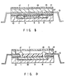
- FIG. 1 is a cross-sectional view of an example of the conventional optical semiconductor module, to which the micromachining is applied.
- the optical semiconductor module comprises an Si substrate 1, an optical fiber 5, an optical semiconductor element 6, an IC 7 for driving the optical semiconductor element 6, and a bonding wire 17.
- the module further comprises an airtight sealing cap 28, a position adjusting groove 2, an airtight sealing solder 10 for connecting the airtight sealing cap 28 with the Si substrate 1, the airtight sealing solder 16, a solder 18 for the optical semiconductor element 6 on the Si substrate 1, an electrical wiring conductor 26 and an insulator 27.
- the optical fiber 5 is fixed to the position adjusting groove 2 of the Si substrate 1, so that the positional relationship to the optical semiconductor element 6 can be mechanically self-alignment. Therefore, optical coupling can be achieved through mechanical assembling steps of mounting the optical semiconductor element 6 to the Si substrate 1 and inserting the optical fiber 5 to the position adjusting groove 2.
- the reason why the mounting base is formed of the Si substrate 1 is that the position adjusting groove 2 can be machine-processed by the aforementioned micromachining.
- an Si monocrystalline (single-crystalline) substrate can be anisotropically etched due to crystal orientation, it can be processed into various geometric shapes.
- a typical shape of a groove for the optical semiconductor module is a so-called V groove having slants of (111) planes on both sides, obtained in a case where a slit-like mask in ⁇ 110> or ⁇ -110> direction is formed on the (100) crystalline plane.
- Monocrystalline Si has a characteristic that the (111) plane is etched much more slowly than the crystalline planes (100) and (110), when etched by an aqueous solution of KOH or hydrazine.
- the reference numerals (100), (110), and (111) denote the crystalline plane.
- the reference numerals ⁇ 110> and ⁇ -110> denote the crystal axis.
- a V groove can be easily formed utilizing the crystal orientation and the mask used in the etching can be formed in the conventional semiconductor process.
- Thermal oxidation SiO 2 obtained by heat-treating an Si substrate in an oxide atmosphere or an Si 3 N 4 by CVD (Chemical Vapor Deposition) method is used as a mask in the etching. It is fully possible that the machine processing accuracy obtained by the system is as low as 1 ⁇ m, depending on etching conditions and setting of the mask.
- the optical semiconductor module to which the micromachining is applied, is effective to omit adjustment of the optical coupling.
- an airtight sealing mechanism of the optical semiconductor element is not necessarily taken into consideration.
- an airtight sealing cap for sealing an optical semiconductor element mounting region, is mounted on an Si substrate formed by the micromachining process, thereby achieving partial airtight sealing on the Si substrate.
- This example is applied to the aforementioned optical semiconductor module utilizing the micromachining, so that the structure shown in FIG. 1 can be easily obtained.
- the optical semiconductor element and the optical fiber can be optically coupled with each other by mechanical assembling, and airtight sealing of the optical semiconductor element can be achieved.
- the cost of producing optical semiconductor modules can be reduced and the production yield can be considerably improved, so that the above-described effects can be obtained.
- the optical semiconductor module thus obtained, still having drawbacks from the viewpoint of the practical use, cannot be used in practice. More specifically, in the structure of FIG. 1, an Si substrate is used as a mount base to make the best use of advantages of the semiconductor process technique. However, if the airtight sealing cap 28 is formed of a metal selected to secure airtightness, the thermal expansion characteristic of the Si substrate is not necessarily conform to those of the other members.
- thermal deformation stress applied to the Si substrate is not negligible, since the area of the Si substrate is increased due to the increase of the number of wiring leaders and the accumulated amount of thermal deformation of the wiring leaders.
- the thermal deformation results in problems, such as a crack of the Si substrate or package leak due to degradation of the mechanical strength of the airtight sealing portion. Such a problem is liable to lower the reliability of the optical semiconductor module. As a result, the yield in consideration of the reliability is lowered and the advantage obtained by simplification and reduction of the optical coupling steps is lost.
- the above problem of low reliability mainly results from the mechanical fragility of Si, the material of the substrate. If, therefore, the substrate is made of ceramics like the general semiconductor package, the problem of low reliability is diminished. However, if the substrate is made of ceramics, various problems arise and the essential object of improving the module is missed. For example, since crystal anisotropy cannot be utilized in the etching process, the accuracy of the etching process is as low as several tens of microns. In addition, the cost of the material of the substrate is increased, or the thermal conductivity of the substrate is lowered. Therefore, it is necessary to give priority to the mechanical workability which is required to omit the adjustment of the optical axis in the optical semiconductor modules. For this reason, use of an Si substrate is indispensable.
- the conventional optical semiconductor module has a limit in reduction of the cost due to the adjustment of the optical axis, whereas application of the micromachining technique, as means for reducing the cost, lacks practicality.
- thermal deformation stress applied to the Si substrate is not negligible, since the area of the Si substrate is increased due to the increase of the number of wiring leaders and the accumulated amount of thermal deformation of the wiring leaders.
- the thermal deformation results in problems, such as cracking of the Si substrate or package leak due to degradation of the mechanical strength of the airtight sealing portion.
- Such a problem is liable to lower the reliability of the optical semiconductor module.
- the yield in consideration of the reliability is lowered and the advantage obtained by simplification and reduction of the optical coupling steps is lost.
- a first object of the present invention is to provide a method of producing an optical semiconductor module, which avoids cracking of the monocrystalline substrate due to thermal deformation stress on account of the airtight sealing member, so that the productivity and reliability can be improved.
- the optical semiconductor element can be optically coupled with the optical waveguide body, such as an optical fiber, only by mechanical assembling, the cost for optical axis adjustment is not required and the reliability of the airtight sealing structure is ensured.
- the present invention is advantageous in that the manufacturing cost is considerably reduced and the application range is widened.
- the bent can be reduced or set off by the reinforcing body or reinforcing member formed on the rear surface of the monocrystalline substrate. Therefore, the monocrystalline substrate is not cracked.
- An example of a optical semiconductor module useful for understanding the present invention comprises an Si substrate 1, i.e., a mount base, as shown in FIG. 2.
- An optical semiconductor element 6 and an IC 7 for transmitting or receiving data to or from the optical semiconductor element are mounted on one surface of the Si substrate 1 via solder.
- An optical axis alignment mechanism is formed on the surface of the Si substrate 1 by the known semiconductor processing technique.
- the optical axis alignment mechanism includes a guide groove 2 of an optical fiber 5, a portion for defining the mounting position of the optical semiconductor element 6, a metallize and the like.
- the Si substrate 1 has a solder groove 3, which is filled with airtight sealing solder 10 surrounding an optical fiber 5.
- the optical semiconductor module comprises a reinforcing plate 8 for preventing the Si substrate 1 from thermal deformation.
- the reinforcing plate 8 is a box having a bottom surface 8a for receiving the Si substrate 1 and walls on the three sides of the bottom. One end of the reinforcing plate 8 does not have a wall so that optical fibers 5 can be drawn out.
- the reinforcing plate 8 is need not be plate-shaped, but can be prismatic reinforcing members. A structure as shown in FIG. 4 or 5 can be used as the reinforcing plate 8.
- the optical semiconductor module of this example comprises an airtight sealing member.
- the airtight sealing member is arranged over the Si substrate 1 and the reinforcing plate 8.
- the airtight sealing member comprises a lower frame 11, an airtight sealing insulator 12, an electrical signal pin 13, an airtight sealing insulator 14, an upper frame 15 and an airtight sealing cap 16.
- the electrical signal pin 13 is extended from first end portions of the Si substrate 1 and the reinforcing plate 8.
- the electrical signal pin 13 is connected to the IC 7 through a bonding wire 17.
- the optical semiconductor element 6 is connected to the IC 7 also through a bonding wire 17.
- the optical semiconductor element 6 is optically coupled with the optical fiber 5.
- the Si substrate having a mechanism for mechanically adjusting an optical axis, is mounted on the reinforcing plate 8 and the airtight sealing member is provided thereon.
- the optical semiconductor element 6 is sealed airtight by sealing the bottom of the airtight sealing member with the Si substrate 1. Thermal deformation of the Si substrate 1 and the upper frame 15 of the airtight sealing member is minimized by using suitable material and structure of the reinforcing member 8.
- the following table shows the combination of the materials of the reinforcing plate and the sealing member (the sealing cap, the upper frame, the lead frame, the airtight sealing insulator and the lower frame).
- the following case A is employed as the reinforcing plate and the sealing member of this example.
- Thermal deformation of the Si substrate 1 and the airtight sealing member (11 to 16) generally occurs in a step of assembling an optical semiconductor module or a reflow soldering step in process of mounting the module on a circuit board. However, it can occur even after the module is mounted on the circuit board, due to an internal temperature distribution on the apparatus in which the circuit board is mounted, or a change in the ambient temperature.
- the most simple method for suppressing the thermal deformation due to the distribution or change of the temperature is as follows: using the same material to form the parts (11 to 16) of the airtight sealing member, particularly, the frames 11 and 15 and the airtight sealing cap 16 (which are generally formed of metal), using the reinforcing plate 8 made of the same material and of the same shape as the airtight sealing member (11 to 16), and connecting the airtight sealing member and the reinforcing plate 8 in the portions facing each other.
- the thermal deformation which occurs between the airtight sealing member (11 to 16) and the substrate Si is set off by the thermal deformation which occurs between the reinforcing plate 8 and the Si substrate 1.
- the problem of the conventional art i.e., a crack of the Si substrate or package leak due to fatigue of the airtight sealing portion, does not easily occur.
- the heat resistance between the Si substrate 1 and the reinforcing plate 8 tends to be high, since the reinforcing member 8 is in contact with the Si substrate 1 only under the airtight sealing portion.
- the reinforcing plate 8 it is possible to make the reinforcing plate 8 be entirely in contact with the lower surface of the Si substrate 1, as shown in FIG. 2, thereby lowering the heat resistance and to adjust the material and the thickness of the reinforcing plate 8 and the characteristics of the solder.
- the thermal deformation can be set off in the same manner as in the aforementioned method.
- the rear end and side ends of the reinforcing plate 8 may be directly bonded with the lower frame 11 of the airtight sealing member.
- deformation between the airtight sealing member and the reinforcing plate 8 is directly compensated, thereby increasing the degree of freedom in thermal deformation minimizing design.
- the Si substrate 1 does not expose to the package exterior, protection thereof is ensured.
- FIGS. 7A and 7B are perspective views showing part of the Si substrate 1 to be mounted on the optical semiconductor module.
- a metallize pattern 4 for achieving soldered joint with the airtight sealing member 11 is formed on the Si substrate 1 as shown in FIG. 6.
- the metallize pattern 4 is formed by pattern forming through deposition of Au/Pt/Ti and lift-off thereof.
- the optical semiconductor element 6 and the IC 7 are mounted on a pad metal having the same structure as that of the metallize pattern 4 and a solder (an Au-Sn solder formed by multiplayer deposition of Au and Sn) formed on the Si substrate, and then subjected to a heat treatment, thereby connecting the element 6 and the IC 7 with the substrate.
- solder groove 3 is to cause solder to flow on the rear side of the optical fiber 5, when the airtight sealing member is soldered with the substrate.
- the solder groove 3 is formed by anistrophic etching of Si in the same manner as in the process of forming the guide groove 2 for adjusting the position of the optical fiber.
- FIG. 7A shows the shape of a mask
- FIG. 7B shows the shape of resulting etched portion 308, 309.
- the narrower portion (307) of the mask is for forming the guide groove 2
- the wider portion (306) is for forming the solder groove 3.
- FIGS 7A and 7B show a case in which the wider groove 308 is etched first using the mask 306, and thereafter, the narrower groove 309 is formed using the mask 307.
- the wider groove 308 is first formed independently, even if the bottom of the wider groove is not completely etched so as to be surrounded by (111) planes, etching deformation does not occur, unless the mask for forming the second groove is not broken.
- the mask pattern of the narrower groove should not intersect with that of the wider groove, but instead a much narrower groove be formed in an end portion of the narrower groove so as to connect it to the slant face of the wider groove.
- a projection is formed in the mask 307 of the narrower groove and an etch back region is formed under the mask.
- the etch back region is stopped by a (111) plane extended from the narrower groove on an extension line of a longer side of the mask 307.
- the distal end of the narrowest groove pattern be located on the (111) plane on the side of the wider groove 306 and project from an end 309 of the bottom of the narrower groove 307 toward the wider groove side, so as not to reach the bottom of the wider groove, to prevent deformation of the bottom of the wider groove 308 as described above.
- a substantially complete composite groove as shown in FIG. 7B is formed.
- FIGS. 8 and 9 are cross-sectional views of the Si substrate 1 as described above, on a plane perpendicular to the plane of FIG. 2.
- FIG. 8 shows a cross section in a portion of the solder groove 3 shown in FIG. 6, and FIG. 9 shows a cross section in a portion of the IC 7 for transmitting or receiving data to or from the optical semiconductor element.
- the side ends of the reinforcing plate 8 are bonded with the lower frame 11 of the airtight sealing member.
- FIGS. 2 and 8 clearly show that the upper surface of the Si substrate 1 is sealed airtight.
- the optical fiber 5 is led outside through the sealed portion in the solder groove 3.
- the optical semiconductor element 6 and the optical fiber 5 are optically coupled with each other on the Si substrate 1 through the mechanical positioning, thereby ensuring airtightness of the optical semiconductor element 6 and the mechanical strength of the Si substrate 1.
- the optical semiconductor element 6 is sealed airtight and the Si substrate 1 is structurally reinforced without incurring an extra producing cost for optical axis adjustment. It is therefore possible to produce a reliable optical semiconductor module at a low cost.
- the Si substrate 1 which is a precision processed element, can be mass-produced through semiconductor processes, it is possible to mass-produce optical semiconductor modules without limit by the throughput or cost of precision processed elements.
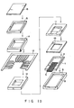
- FIG. 10 is an exploded view of the example shown in FIG. 2. Details of the elements, such as the semiconductor element, are not shown or described in the following.
- the lower frame 11 made of Kovar alloy, has a partially modified optical fiber inserting portion.
- the sealing insulators 12 and 14 are made of, for example, low melting point glass.
- the electrical signal pin 13, the upper frame 15 and the airtight sealing cap 16, as well as the lower frame 11, are made of the Kovar alloy.
- the optical fibers can be soldered as shown in FIG. 8. If the lower frame 11 does not have the modified portion, the sealing solder 10 must be considerably thick to achieve airtight sealing, in which case the solder material may flow out or the width of the soldered portion may be different from place to place. In addition, since the lower frame 11 is liable to be brought into contact with the optical fiber 5, stress is easily applied to the optical fiber 5 when the module is assembled. In an extreme case, the optical fiber 5 may be damaged or cut off, in which case the reliability and the yield of the modules will be lowered. The same problem arises in a case where the optical fiber is replaced with an optical wave guide.
- the process of assembling the module is as follows. First, the lower frame 11, the sealing insulators 12 and 14, the lead frame (the electrical signal pin) 13 and the upper frame 15 are accumulated together and subjected to a heat treatment, thereby forming the aforementioned airtight sealing member as a unit. Then, the optical semiconductor element 6, the IC 7 and the optical fiber 5 are successively or simultaneously mounted on the Si substrate 1 by, for example, soldering. A preform solder 9, the Si substrate 1, the airtight sealing solder 10 and the airtight sealing member (the accumulated member consisting of the parts 11 to 15) are successively accumulated, and the preform solder 9 and the sealing solder 10 are simultaneously caused to reflow. Thereafter, the semiconductor element and the electrical pin 13 are wire-bonded and then, the sealing cap 16 is sealed by means of seam welding. As a result, the optical semiconductor module as shown in FIG. 2 is obtained.
- the optical semiconductor element can be optically coupled with an optical waveguide, such as an optical fiber, and the optical semiconductor element can be airtight sealed only by a mechanical assembling process. Moreover, since the reinforcing plate is attached on the rear surface of the Si substrate, the Si substrate can be prevented from crack due to the stress of the airtight sealing cap.
- the present invention allows reduction in manufacturing cost of the semiconductor module, substantial improvement of the productivity thereof, and assured reliability.
- the present invention also allows a large-capacity and high-quality signal transmission, which has been characteristic to the optical communication technology, to be applied to general industry equipment.
Landscapes
- Physics & Mathematics (AREA)
- General Physics & Mathematics (AREA)
- Optics & Photonics (AREA)
- Optical Couplings Of Light Guides (AREA)
- Led Device Packages (AREA)
- Light Receiving Elements (AREA)
Claims (1)
- Procédé de production d'un module optique à semiconducteur, caractérisé en ce qu'un motif composite d'une combinaison de rainures ayant des largeurs différentes est formé sur un plan (100) d'un substrat en Si (1) par une gravure anisotrope, dans lequel la gravure est sensiblement arrêtée au niveau du plan (111), puis une fibre optique (5) est fixée sur le motif composite, caractérisé en ce que ledit procédé comprend les étapes séquentielles consistant à :former une rainure plus large en gravant le substrat en Si (1), en utilisant un premier masque à fenêtre rectangulaire ; etformer une rainure plus étroite destinée à supporter une fibre optique en gravant le substrat en Si (1), en utilisant un masque comprenant une seconde fenêtre rectangulaire, située à une distance prédéterminée de la rainure plus large, et comprenant en outre une fenêtre en forme de bande qui est plus étroite que la seconde fenêtre rectangulaire et qui s'étend depuis une face inclinée sur une partie de contact de la rainure plus large vers la seconde fenêtre rectangulaire.
Applications Claiming Priority (3)
| Application Number | Priority Date | Filing Date | Title |
|---|---|---|---|
| JP231947/94 | 1994-09-28 | ||
| JP23194794A JP3345518B2 (ja) | 1994-09-28 | 1994-09-28 | 光半導体モジュールの製造方法 |
| JP23194794 | 1994-09-28 |
Publications (3)
| Publication Number | Publication Date |
|---|---|
| EP0704731A2 EP0704731A2 (fr) | 1996-04-03 |
| EP0704731A3 EP0704731A3 (fr) | 1999-09-22 |
| EP0704731B1 true EP0704731B1 (fr) | 2008-01-16 |
Family
ID=16931564
Family Applications (1)
| Application Number | Title | Priority Date | Filing Date |
|---|---|---|---|
| EP95306729A Expired - Lifetime EP0704731B1 (fr) | 1994-09-28 | 1995-09-25 | Module optique à semi-conducteur et procédé pour sa fabrication |
Country Status (4)
| Country | Link |
|---|---|
| US (1) | US5719979A (fr) |
| EP (1) | EP0704731B1 (fr) |
| JP (1) | JP3345518B2 (fr) |
| DE (1) | DE69535688T2 (fr) |
Families Citing this family (43)
| Publication number | Priority date | Publication date | Assignee | Title |
|---|---|---|---|---|
| US5692084A (en) * | 1996-06-11 | 1997-11-25 | The Whitaker Corporation | Package for an optoelectronic device |
| JP3758258B2 (ja) * | 1996-11-29 | 2006-03-22 | 富士通株式会社 | 光結合装置 |
| JPH10223505A (ja) * | 1997-02-05 | 1998-08-21 | Oki Electric Ind Co Ltd | ホトリソグラフィ用マスクアライメントマークの形成方法 |
| SG71172A1 (en) * | 1997-12-03 | 2000-03-21 | Sumitomo Electric Industries | Optical data link |
| IL123207A0 (en) * | 1998-02-06 | 1998-09-24 | Shellcase Ltd | Integrated circuit device |
| US6872984B1 (en) * | 1998-07-29 | 2005-03-29 | Silicon Light Machines Corporation | Method of sealing a hermetic lid to a semiconductor die at an angle |
| US6146025A (en) * | 1998-08-03 | 2000-11-14 | Litton Systems Inc. | Laser diode and substrate |
| US6521989B2 (en) * | 1998-10-08 | 2003-02-18 | Honeywell Inc. | Methods and apparatus for hermetically sealing electronic packages |
| JP3459787B2 (ja) | 1999-04-02 | 2003-10-27 | Nec化合物デバイス株式会社 | 光半導体モジュール及びその製造方法 |
| US6445837B1 (en) | 1999-03-31 | 2002-09-03 | Nu-Wave Photonics, Inc. | Hybrid opto-electronic circuits and method of making |
| US6168963B1 (en) * | 1999-06-21 | 2001-01-02 | Lucent Technologies, Inc. | System for adhering parts |
| US20070181781A1 (en) * | 2001-03-06 | 2007-08-09 | Digital Optics Corporation | Integrated optical transceiver |
| IL133453A0 (en) * | 1999-12-10 | 2001-04-30 | Shellcase Ltd | Methods for producing packaged integrated circuit devices and packaged integrated circuit devices produced thereby |
| US6775440B2 (en) * | 2000-04-28 | 2004-08-10 | Kyocera Corporation | Optical module and carrier for optical module |
| US6624507B1 (en) * | 2000-05-09 | 2003-09-23 | National Semiconductor Corporation | Miniature semiconductor package for opto-electronic devices |
| JP3436243B2 (ja) * | 2000-09-04 | 2003-08-11 | 住友電気工業株式会社 | 光半導体気密封止容器及びそれを用いた光半導体モジュール |
| US6845189B2 (en) * | 2000-11-15 | 2005-01-18 | Telefonaktiebolaget Lm Ericsson (Publ) | System and a method for limiting the maximum of light transmitted from a ribbon fiber |
| GB2372633A (en) * | 2001-02-24 | 2002-08-28 | Mitel Semiconductor Ab | Flip-chip mounted optical device |
| WO2002079812A2 (fr) * | 2001-03-28 | 2002-10-10 | Iljin Corporation | Module optique de taille reduite |
| US6514783B1 (en) * | 2001-09-17 | 2003-02-04 | Applied Micro Circuits Corporation | Method for determining a layout for a flip-chip transition interface structure |
| US6639322B1 (en) * | 2001-09-17 | 2003-10-28 | Applied Micro Circuits Corporation | Flip-chip transition interface structure |
| US7832177B2 (en) * | 2002-03-22 | 2010-11-16 | Electronics Packaging Solutions, Inc. | Insulated glazing units |
| US6962834B2 (en) | 2002-03-22 | 2005-11-08 | Stark David H | Wafer-level hermetic micro-device packages |
| US20060191215A1 (en) * | 2002-03-22 | 2006-08-31 | Stark David H | Insulated glazing units and methods |
| US6627814B1 (en) * | 2002-03-22 | 2003-09-30 | David H. Stark | Hermetically sealed micro-device package with window |
| JP4085697B2 (ja) * | 2002-05-29 | 2008-05-14 | 住友電気工業株式会社 | 光リンクモジュール |
| US7033664B2 (en) | 2002-10-22 | 2006-04-25 | Tessera Technologies Hungary Kft | Methods for producing packaged integrated circuit devices and packaged integrated circuit devices produced thereby |
| DE112004003069B4 (de) * | 2003-04-30 | 2017-01-19 | Fujikura Ltd. | Optisches Verbindungsstück |
| WO2004097480A1 (fr) * | 2003-04-30 | 2004-11-11 | Fujikura Ltd. | Ensemble connecteur optique, support de connecteur, connecteur optique |
| JP4685366B2 (ja) * | 2004-04-13 | 2011-05-18 | パナソニック株式会社 | 光学部品の接合方法 |
| JP2015060097A (ja) * | 2013-09-19 | 2015-03-30 | ソニー株式会社 | 光伝送モジュール |
| GB2422682B (en) * | 2005-01-31 | 2008-11-12 | Jan Lewandowski | Optical module |
| US7989040B2 (en) | 2007-09-14 | 2011-08-02 | Electronics Packaging Solutions, Inc. | Insulating glass unit having multi-height internal standoffs and visible decoration |
| DE102007046337A1 (de) * | 2007-09-27 | 2009-04-02 | Osram Opto Semiconductors Gmbh | Optoelektronischer Halbleiterchip, optoelektronisches Bauelement und Verfahren zum Herstellen eines optoelektronischen Bauelements |
| DE102008031930B4 (de) * | 2008-07-08 | 2014-09-25 | Rüdiger Lanz | Beleuchtungsvorrichtung mit Mikro-Linsenarray |
| WO2010019484A2 (fr) * | 2008-08-09 | 2010-02-18 | Eversealed Windows, Inc. | Joint d'étanchéité à bord souple asymétrique pour vitrage isolant vis-à-vis du vide |
| WO2010083476A2 (fr) * | 2009-01-15 | 2010-07-22 | Eversealed Windows, Inc | Joint de bordure souple pour unité de vitrage pour isolation sous vide |
| WO2010083475A2 (fr) * | 2009-01-15 | 2010-07-22 | Eversealed Windows, Inc. | Éléments verticaux reliés à des filaments pour maintenir la séparation entre les vitres dans des unités de vitrage pour isolation sous vide |
| WO2011153381A2 (fr) | 2010-06-02 | 2011-12-08 | Eversealed Windows, Inc. | Unité de vitrage à pluralité de vitres comprenant un joint avec une couche de revêtement adhésive et hermétique |
| US9328512B2 (en) | 2011-05-05 | 2016-05-03 | Eversealed Windows, Inc. | Method and apparatus for an insulating glazing unit and compliant seal for an insulating glazing unit |
| JP5956815B2 (ja) * | 2012-04-20 | 2016-07-27 | 日本航空電子工業株式会社 | 光モジュール用基体及び光モジュール |
| DE102014221728A1 (de) * | 2014-10-24 | 2016-04-28 | Technische Universität Dresden | Anordnung elektro-optischer Bauelemente zur optischen Daten- und/oder Energieübertragung in einem Gehäuse |
| JP2023131869A (ja) * | 2022-03-10 | 2023-09-22 | 株式会社東芝 | 並列受信モジュール |
Family Cites Families (20)
| Publication number | Priority date | Publication date | Assignee | Title |
|---|---|---|---|---|
| JPS5433683A (en) * | 1977-07-08 | 1979-03-12 | Hitachi Ltd | Air seal mounting for light emitting element |
| FR2500642B1 (fr) * | 1981-02-24 | 1986-06-06 | Nippon Sheet Glass Co Ltd | Structure de support pour la fixation de fibres optiques et de lentilles et procede pour leur preparation ainsi que dispositif les utilisant |
| JPS62123412A (ja) * | 1985-11-25 | 1987-06-04 | Nec Corp | 光集積回路用パツケ−ジ |
| US4830456A (en) * | 1986-11-15 | 1989-05-16 | Sumitomo Electric Industries, Ltd. | Optical connector and process for producing the same |
| JPH01180506A (ja) * | 1988-01-12 | 1989-07-18 | Sumitomo Electric Ind Ltd | 光コネクタ |
| JPH01219806A (ja) * | 1988-02-29 | 1989-09-01 | Sumitomo Electric Ind Ltd | 光コネクタ |
| US4810557A (en) * | 1988-03-03 | 1989-03-07 | American Telephone And Telegraph Company, At&T Bell Laboratories | Method of making an article comprising a tandem groove, and article produced by the method |
| US4897711A (en) * | 1988-03-03 | 1990-01-30 | American Telephone And Telegraph Company | Subassembly for optoelectronic devices |
| JPH0213911A (ja) * | 1988-07-01 | 1990-01-18 | Nec Corp | 光デバイス |
| JPH02251918A (ja) * | 1989-03-27 | 1990-10-09 | Sumitomo Electric Ind Ltd | 光コネクタ |
| US4930857A (en) * | 1989-05-19 | 1990-06-05 | At&T Bell Laboratories | Hybrid package arrangement |
| DE4013630A1 (de) * | 1989-05-31 | 1990-12-06 | Siemens Ag | Optoelektronischer wandlermodul und verfahren zu dessen herstellung |
| DE58909602D1 (de) * | 1989-09-22 | 1996-03-21 | Siemens Ag | Verfahren zum anisotropen Ätzen von Silizium |
| JPH0486609A (ja) * | 1990-07-27 | 1992-03-19 | Sumitomo Electric Ind Ltd | 光コネクタ |
| WO1993018422A1 (fr) * | 1992-03-07 | 1993-09-16 | Robert Bosch Gmbh | Composant optique integre |
| US5307434A (en) * | 1992-07-16 | 1994-04-26 | At&T Bell Laboratories | Article that comprises a laser coupled to an optical fiber |
| JPH0667036A (ja) * | 1992-08-21 | 1994-03-11 | Nippon Sheet Glass Co Ltd | 光導波路デバイスの耐衝撃構造 |
| US5412748A (en) * | 1992-12-04 | 1995-05-02 | Kabushiki Kaisha Toshiba | Optical semiconductor module |
| US5555333A (en) * | 1993-07-12 | 1996-09-10 | Ricoh Company, Ltd. | Optical module and a fabrication process thereof |
| US5535296A (en) * | 1994-09-28 | 1996-07-09 | Optobahn Corporation | Integrated optoelectronic coupling and connector |
-
1994
- 1994-09-28 JP JP23194794A patent/JP3345518B2/ja not_active Expired - Fee Related
-
1995
- 1995-09-21 US US08/531,640 patent/US5719979A/en not_active Expired - Fee Related
- 1995-09-25 DE DE69535688T patent/DE69535688T2/de not_active Expired - Fee Related
- 1995-09-25 EP EP95306729A patent/EP0704731B1/fr not_active Expired - Lifetime
Also Published As
| Publication number | Publication date |
|---|---|
| EP0704731A3 (fr) | 1999-09-22 |
| JPH0894888A (ja) | 1996-04-12 |
| DE69535688D1 (de) | 2008-03-06 |
| JP3345518B2 (ja) | 2002-11-18 |
| EP0704731A2 (fr) | 1996-04-03 |
| DE69535688T2 (de) | 2009-01-08 |
| US5719979A (en) | 1998-02-17 |
Similar Documents
| Publication | Publication Date | Title |
|---|---|---|
| EP0704731B1 (fr) | Module optique à semi-conducteur et procédé pour sa fabrication | |
| US6345917B2 (en) | Hermetically sealed optical-semiconductor container and optical-semiconductor module | |
| US7086788B2 (en) | Optical sub-assembly for opto-electronic modules | |
| US4920262A (en) | Photoelectric device with leads | |
| US8233757B2 (en) | Wafer based optical chassis and associated methods | |
| US7023705B2 (en) | Ceramic optical sub-assembly for optoelectronic modules | |
| JPH08166523A (ja) | 光アセンブリ | |
| US7125176B1 (en) | PCB with embedded optical fiber | |
| EP1211765B1 (fr) | Boítier hermétique pour un module optique à semi-conducteur et amplificateur à fibre optique | |
| US5026134A (en) | Optical communication apparatus with base for fixing elements | |
| US7146106B2 (en) | Optic semiconductor module and manufacturing method | |
| JPH07199006A (ja) | 光サブアセンブリ及び光モジュール | |
| JP4543561B2 (ja) | 光モジュールの製造方法、及び光モジュール | |
| US7284913B2 (en) | Integrated fiber attach pad for optical package | |
| US7269027B2 (en) | Ceramic optical sub-assembly for optoelectronic modules | |
| EP1014132A2 (fr) | Module optique | |
| JPH1152193A (ja) | 光半導体モジュール | |
| JP2001343561A (ja) | 光モジュール | |
| JP2002232054A (ja) | 光モジュールの実装構造 | |
| JP4798863B2 (ja) | 光電気配線基板 | |
| JP2001127373A (ja) | 光モジュール | |
| US20040264886A1 (en) | Low cost package design for fiber coupled optical component | |
| JPH10117043A (ja) | 発光素子 | |
| EP1953577B1 (fr) | Chassis optique monté sur plaquette | |
| JP2000199831A (ja) | 光モジュ―ル |
Legal Events
| Date | Code | Title | Description |
|---|---|---|---|
| PUAI | Public reference made under article 153(3) epc to a published international application that has entered the european phase |
Free format text: ORIGINAL CODE: 0009012 |
|
| 17P | Request for examination filed |
Effective date: 19951023 |
|
| AK | Designated contracting states |
Kind code of ref document: A2 Designated state(s): DE FR GB |
|
| PUAL | Search report despatched |
Free format text: ORIGINAL CODE: 0009013 |
|
| AK | Designated contracting states |
Kind code of ref document: A3 Designated state(s): DE FR GB |
|
| RIC1 | Information provided on ipc code assigned before grant |
Free format text: 6G 02B 6/42 A, 6G 02B 6/38 B, 6G 02B 6/36 B, 6H 01L 21/308 B |
|
| 17Q | First examination report despatched |
Effective date: 20020222 |
|
| GRAP | Despatch of communication of intention to grant a patent |
Free format text: ORIGINAL CODE: EPIDOSNIGR1 |
|
| RAP1 | Party data changed (applicant data changed or rights of an application transferred) |
Owner name: KABUSHIKI KAISHA TOSHIBA |
|
| GRAS | Grant fee paid |
Free format text: ORIGINAL CODE: EPIDOSNIGR3 |
|
| GRAA | (expected) grant |
Free format text: ORIGINAL CODE: 0009210 |
|
| AK | Designated contracting states |
Kind code of ref document: B1 Designated state(s): DE FR GB |
|
| REG | Reference to a national code |
Ref country code: GB Ref legal event code: FG4D |
|
| REF | Corresponds to: |
Ref document number: 69535688 Country of ref document: DE Date of ref document: 20080306 Kind code of ref document: P |
|
| ET | Fr: translation filed | ||
| PLBE | No opposition filed within time limit |
Free format text: ORIGINAL CODE: 0009261 |
|
| STAA | Information on the status of an ep patent application or granted ep patent |
Free format text: STATUS: NO OPPOSITION FILED WITHIN TIME LIMIT |
|
| PGFP | Annual fee paid to national office [announced via postgrant information from national office to epo] |
Ref country code: FR Payment date: 20080915 Year of fee payment: 14 |
|
| 26N | No opposition filed |
Effective date: 20081017 |
|
| PGFP | Annual fee paid to national office [announced via postgrant information from national office to epo] |
Ref country code: DE Payment date: 20081002 Year of fee payment: 14 |
|
| PGFP | Annual fee paid to national office [announced via postgrant information from national office to epo] |
Ref country code: GB Payment date: 20081001 Year of fee payment: 14 |
|
| GBPC | Gb: european patent ceased through non-payment of renewal fee |
Effective date: 20090925 |
|
| REG | Reference to a national code |
Ref country code: FR Ref legal event code: ST Effective date: 20100531 |
|
| PG25 | Lapsed in a contracting state [announced via postgrant information from national office to epo] |
Ref country code: FR Free format text: LAPSE BECAUSE OF NON-PAYMENT OF DUE FEES Effective date: 20090930 Ref country code: DE Free format text: LAPSE BECAUSE OF NON-PAYMENT OF DUE FEES Effective date: 20100401 |
|
| PG25 | Lapsed in a contracting state [announced via postgrant information from national office to epo] |
Ref country code: GB Free format text: LAPSE BECAUSE OF NON-PAYMENT OF DUE FEES Effective date: 20090925 |