EP0683934B1 - Gleichspannungswandler - Google Patents
Gleichspannungswandler Download PDFInfo
- Publication number
- EP0683934B1 EP0683934B1 EP94906132A EP94906132A EP0683934B1 EP 0683934 B1 EP0683934 B1 EP 0683934B1 EP 94906132 A EP94906132 A EP 94906132A EP 94906132 A EP94906132 A EP 94906132A EP 0683934 B1 EP0683934 B1 EP 0683934B1
- Authority
- EP
- European Patent Office
- Prior art keywords
- winding
- series
- converter according
- windings
- converter
- Prior art date
- Legal status (The legal status is an assumption and is not a legal conclusion. Google has not performed a legal analysis and makes no representation as to the accuracy of the status listed.)
- Expired - Lifetime
Links
- 239000003990 capacitor Substances 0.000 claims abstract description 29
- 238000004804 winding Methods 0.000 claims description 70
- 238000009499 grossing Methods 0.000 claims description 8
- 230000008878 coupling Effects 0.000 claims description 3
- 238000010168 coupling process Methods 0.000 claims description 3
- 238000005859 coupling reaction Methods 0.000 claims description 3
- 238000006243 chemical reaction Methods 0.000 claims description 2
- 230000010287 polarization Effects 0.000 claims 1
- 230000001939 inductive effect Effects 0.000 abstract description 3
- 230000005540 biological transmission Effects 0.000 description 3
- 230000008901 benefit Effects 0.000 description 2
- 230000006872 improvement Effects 0.000 description 2
- 238000011161 development Methods 0.000 description 1
- 230000018109 developmental process Effects 0.000 description 1
- 238000000034 method Methods 0.000 description 1
- 230000009467 reduction Effects 0.000 description 1
- 238000005476 soldering Methods 0.000 description 1
- 230000009466 transformation Effects 0.000 description 1
Images
Classifications
-
- H—ELECTRICITY
- H02—GENERATION; CONVERSION OR DISTRIBUTION OF ELECTRIC POWER
- H02M—APPARATUS FOR CONVERSION BETWEEN AC AND AC, BETWEEN AC AND DC, OR BETWEEN DC AND DC, AND FOR USE WITH MAINS OR SIMILAR POWER SUPPLY SYSTEMS; CONVERSION OF DC OR AC INPUT POWER INTO SURGE OUTPUT POWER; CONTROL OR REGULATION THEREOF
- H02M3/00—Conversion of DC power input into DC power output
- H02M3/005—Conversion of DC power input into DC power output using Cuk converters
-
- H—ELECTRICITY
- H02—GENERATION; CONVERSION OR DISTRIBUTION OF ELECTRIC POWER
- H02M—APPARATUS FOR CONVERSION BETWEEN AC AND AC, BETWEEN AC AND DC, OR BETWEEN DC AND DC, AND FOR USE WITH MAINS OR SIMILAR POWER SUPPLY SYSTEMS; CONVERSION OF DC OR AC INPUT POWER INTO SURGE OUTPUT POWER; CONTROL OR REGULATION THEREOF
- H02M3/00—Conversion of DC power input into DC power output
- H02M3/02—Conversion of DC power input into DC power output without intermediate conversion into AC
- H02M3/04—Conversion of DC power input into DC power output without intermediate conversion into AC by static converters
- H02M3/10—Conversion of DC power input into DC power output without intermediate conversion into AC by static converters using discharge tubes with control electrode or semiconductor devices with control electrode
- H02M3/145—Conversion of DC power input into DC power output without intermediate conversion into AC by static converters using discharge tubes with control electrode or semiconductor devices with control electrode using devices of a triode or transistor type requiring continuous application of a control signal
- H02M3/155—Conversion of DC power input into DC power output without intermediate conversion into AC by static converters using discharge tubes with control electrode or semiconductor devices with control electrode using devices of a triode or transistor type requiring continuous application of a control signal using semiconductor devices only
Definitions
- the invention relates to a clocked DC converter with a conversion transformer according to the preamble of the main claim.
- Such a DC converter is also known from IEEE Transactions on Industrial Electronics, Vol. 36, No. 4, Nov. 1989, S568-578.
- the DC-DC converter according to the invention with the characterizing features of the main claim has the advantage that only the converter transformer is required as the only inductive component. In addition to the resulting reduction in component size, there is the additional advantage that the power transmission to the output is not only capacitive, but also that magnetic energy is also transmitted via the converter transformer becomes. This leads to better efficiency when using a low-voltage transistor with low forward losses.
- By designing the converter transformer an output current with very little ripple can be achieved, which results in the possibility of using a smaller output capacitor.
- the circuit breaker is opened, the voltage at this circuit breaker overshoots less, which leads to lower switching losses and a lower voltage reserve.
- the output has a current source character. this means that the output current is limited when the load changes.
- the voltage on the third winding must always be polarized so that the smoothing capacitor is not discharged during the charging phase of the series capacitor.
- the number of turns (n3) of the third winding essentially corresponds to the sum of the number of turns (nl. N2) of the first and second windings.
- all three windings must be coupled very well.
- the windings are advantageously wound in parallel, the division into the three individual windings and their respective polarity being formed by appropriate wiring of the winding ends.
- a multi-strand HF strand has proven particularly useful for winding. In order to make the resistance of the first winding as low as possible, it has a plurality of parallel winding strands. In order to easily double or triple the number of turns for the other windings, winding strands wound in parallel are connected in series. By optimizing the The stray inductance is reduced by the transformer and thus the switching losses at the switching transistor are reduced.
- a ratio of the number of turns (n1, n2, n3) of the three windings of essentially 1: 2: 3 has proven particularly useful.
- a fast power transistor in particular a MOSFET, is preferably used as the power switch. This can be clocked as a function of time and / or current.
- a fast high-voltage diode is advantageously used as the diode.
- the series capacitor should be of high quality.
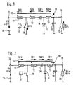
- the DC-DC converter shown in FIGS. 1 and 2 has a converter transformer 10 which has a first winding 11, a second winding 12 and a third winding 13 has.
- the first winding 11 and the second winding 12 form a divided primary winding, while the third winding 13 represents a secondary winding.
- An input voltage Ub of, for example, 10 volts lies between a first input terminal 14 connected to the first winding 11 and a second input terminal 15 connected to ground.
- the connection point between the first winding 11 and the second winding 12 is connected to ground via a power switch 16 designed as a power transistor .
- the commercially available IRLZ 44 power MOSFET is suitable as a circuit breaker, for example.
- the circuit breaker 16 is clocked by means of a switching circuit 17.
- this clocking is clocked by a control voltage with a fixed test ratio. This is particularly possible. if there is a fixed relationship between input voltage and output voltage. In general, however, the clocking is done in this way. that either the circuit breaker 16 is closed until a certain value of the current flowing through is reached, and then a constant opening time follows. Another option is to set a fixed closing time and to start the next closing time when the current has dropped to a certain value. for example to zero.
- connection of the second winding 12 facing away from the first winding 11 is connected to an output terminal 19 via the series connection of a series capacitor 18 with the third winding 13 which is polarized opposite to the first two windings 11, 12, a smoothing capacitor 20 being connected between this and ground .
- a diode 21 connected as a high-voltage diode is between the Connection point between the series capacitor 18 connected to the third winding 13 and ground.
- a magnetic core or transformer core 22 is shown schematically and carries the three windings 11, 12, 13.
- the output voltage Ua at the smoothing capacitor 20 of, for example, -150 volts can be applied to a schematically illustrated consumer 23.
- the three windings 11-13 are wound in parallel, for example using a 9-strand HF strand.
- the three windings 11-13 are then formed by soldering the 18 free ends of the HF strand accordingly.
- 4 strands of the strand are connected in parallel.
- the second winding 12 should have a double number of turns. which is achieved by connecting 2 additional strings in series.
- the third winding 13 should have a number of turns three times that of the first winding 11. which is achieved by connecting 3 additional strings in series.
- a further improvement in the coupling factor can be achieved by stranding the individual wires.
- an input voltage of 10 volts is assumed, that is, for example, the battery voltage of a motor vehicle.
- a negative DC voltage of -150 volts is to be formed as the output voltage Ua.
- the number of turns (n1, n2, n3) of the three windings 11-13 behave as 1: 2: 3. In principle, other conditions could also exist.
- the circuit breaker 16 is closed.
- the first winding 11 is therefore connected to the input voltage Ud, the current through the first winding rises and energy is stored in this first winding.
- the current of the circuit breaker 16 commutates to the second winding 12 and charges the series capacitor 18 via the conductive diode 21 to a positive voltage of 160 volts in the example.
- the circuit breaker 16 is now closed again, the first winding 11 is again at the input voltage Ub, the left side of the series capacitor 18 is at a voltage of -2 via the second winding 12 and the power switch 16.
- Ub So to -20 volts, since the partial transformer formed from the windings 11 and 12 has a transformation ratio of 2.
- the diode 21 has a negative voltage of -180 volts, so that it blocks.
- the smoothing capacitor 20 is now above the voltage induced in the third winding 13 of -30 volts - the partial transformer formed from the first winding 11 and the third winding 13 has a transmission ratio of 3 - at this negative voltage. This results in an output voltage Ua of -150 volts (the negative capacitor voltage across the series capacitor 18 reduced by the input voltage Ub).
- the voltage on the third winding 13 is always polarized so that the smoothing capacitor 20 is not discharged during the charging phase of the series capacitor 18.
- the series capacitor 18 should have the smallest possible loss factor because of the AC load.
Landscapes
- Engineering & Computer Science (AREA)
- Power Engineering (AREA)
- Dc-Dc Converters (AREA)
Abstract
Description
- Die Erfindung betrifft einen getakteten Gleichspannungswandler mit einem Wandlungstransformator nach der Gattung des Hauptanspruchs.
- In dem IEEE Report "IAS Annual Meeting" 2.-6. Oktober 1977. Los Angeles, S. 1113. ist ein derartiger Gleichspannungswandler beschrieben. der als Abwärtswandler ausgebildet ist und bei dem ein Transformatorkern nur zwei Wicklungen besitzt. Die Verbindung zum ausgangsseitigen Glättungskondensator erfolgt über eine separate Drossel. Hierdurch, sind zum einen zwei induktive Bauelemente erforderlich. und zum anderen kann die Leistungsübertragung zum Ausgang hin nur kapazitiv erfolgen.
- Zur derartiger Gleichspannungswandler ist auch aus den IEEE Transactions on Industrial Electronics, Vol. 36, Nr.4, Nov. 1989, S568-578 bekannt.
- Der erfindungsgemäße Gleichspannungswandler mit den kennzeichnenden Merkmalen des Hauptanspruchs hat demgegenüber den Vorteil, daß als einziges induktives Bauelement lediglich der Wandlertransformator erforderlich ist. Neben der hierdurch bewirkten Bauteilreduzierung tritt der zusätzliche Vorteil auf, daß die Leistungsübertragung zum Ausgang nicht nur kapazitiv erfolgt, sondern daß zusätzlich auch magnetische Energie über den Wandlertransformator übertragen wird. Dies führt zu einem besseren Wirkungsgrad bei Verwendung eines Niedervolt-Transistors mit geringen Durchlaßverlusten. Durch die Ausbildung des Wandlertransformators ist ein Ausgangsstrom mit sehr geringer Welligkeit erreichbar, wodurch sich die Möglichkeit ergibt, einen kleineren Ausgangskondensator zu verwenden. Beim Öffnen des Leistungsschalters erfolgt ein geringeres Überschwingen der Spannung an diesem Leistungsschalter, was zu geringeren Schaltverlusten führt und eine geringere Spannungsreserve möglich macht. Der Ausgang weist einen Stromquellencharakter auf. das heißt, der Ausgangsstrom wird bei Lastwechsel begrenzt.
- Durch die in den Unteransprüchen aufgeführten Maßnahmen sind vorteilhafte Weiterbildungen und Verbesserungen des im Hauptanspruch angegebenen Gleichspannungswandlers möglich.
- Die Spannung an der dritten Wicklung muß immer so gepolt sein, daß während der Aufladephase des Längskondensators der Glättungskondensator nicht entladen wird. Dies wird dadurch erreicht, daß die Windungszahl (n3) der dritten Wicklung im wesentichen der Summe der Windungszahlen (nl. n2) der ersten und zweiten Wicklung entspricht. Weiterhin müssen alle drei Wicklungen sehr gut gekoppelt sein. Hierzu werden die Windungen in vorteilhafter Weise parallel gewickelt, wobei die Aufteilung in die drei einzelnen Wicklungen und deren jeweilige Polarität durch entsprechende Beschaltung der Wicklungsenden gebildet wird. Für die Wicklung hat sich eine viel-strängige HF-Litze besonders bewährt. Um den Widerstand der ersten Wicklung möglichst gering zu machen, weist diese mehrere parallele Wicklungsstränge auf. Um auf einfache Weise die Windungszahlen für die anderen Wicklungen zu verdoppeln bzw. zu verdreifachen, werden bei diesen parallel gewickelte Wicklungsstränge in Reihe geschaltet. Durch eine solche Optimierung des Transformators wird die Streuinduktivität reduziert und damit die Schaltverluste am Schalttransistor reduziert.
- Besonders bewährt hat sich ein Verhältnis der Windungszahlen (n1, n2, n3) der drei Wicklungen von im wesentlichen 1 : 2 : 3.
- Als Leistungsschalter wird vorzugsweise ein schneller Leistungstransistor eingesetzt, insbesondere ein MOSFET. Dieser kann zeit- und/oder stromabhängig getaktet werden.
- Als Diode wird in vorteilhafter Weise eine schnelle Hochvoltdiode verwendet. Der Längskondensator sollte eine hohe Güte aufweisen.
- Ein Ausführungsbeispiel der Erfindung ist in der Zeichnung dargestellt und in der nachfolgenden Beschreibung näher erläutert. Es zeigen:
- Fig. 1
- eine Schaltungsausführung des ersten Ausführungsbeispiels, bei dem die Spannungsverhältnisse bei geöffnetem Leistungstransistor dargestellt sind, und
- Fig. 2
- dasselbe Ausführungsbeispiel, bei dem die Spannungsverhältnisse bei geschlossenem Leistungstransistor dargestellt sind.
- Der in den Fig. 1 und 2 dargestellte Gleichspannungswandler besitzt einen Wandlertransformator 10, der eine erste Wicklung 11, eine zweite Wicklung 12 und eine dritte Wicklung 13 aufweist. Dabei bilden die erste Wicklung 11 und die zweite Wicklung 12 eine geteilte Primärwicklung, während die dritte Wicklung 13 eine Sekundärwicklung darstellt. Eine Eingangsspannung Ub von beispielsweise 10 Volt liegt zwischen einer mit der ersten Wicklung 11 verbundenen ersten Eingangsklemme 14 und einer mit Masse verbundenen zweiten Eingangsklemme 15. Der Verknüpfungspunkt zwischen der ersten Wicklung 11 und der zweiten Wicklung 12 liegt über einen als Leistungstransistor ausgebildeten Leistungsschalter 16 an Masse. Als Leistungsschalter eignet sich beispielsweise der im Handel erhältliche Leistungs-MOSFET IRLZ 44.
- In an sich bekannter Weise wird der Leistungsschalter 16 mittels einer Tektschaltung 17 getaktet. Im einfachsten Falle wird diese Taktung durch eine Steuerspannung mit einem festen Testverhältnis getaktet. Dies ist insbesondere dann möglich. wenn ein festes Verhältnis zwischen Eingangsspannung und ausgangsspannung vorliegt. Im allgemeinen wird die Taktung jedoch so vorgenommen. daß entweder der Leistungsschalter 16 geschlossen ist, bis ein bestimmter Wert des durchfließenden Stroms erreicht wird, und es schließt sich dann eine konstante Öffnungszeit an. Eine andere Möglichkeit besteht darin, eine feste Schließzeit vorzugeben, und die nächste Schließzeit dann zu starten, wenn der Strom auf einen bestimmten Wert abgesunken ist. beispielsweise auf den Wert Null.
- Der von der ersten Wicklung 11 abgewandte Anschluß der zweiten Wicklung 12 ist über die Reihenschaltung eines Längskondensators 18 mit der entgegengesetzt zu den ersten beiden Wicklungen 11, 12 gepolten dritten Wicklung 13 an eine Ausgangsklemme 19 angeschlossen, wobei zwischen dieser und Masse ein Glättungskondensator 20 geschaltet ist. Eine als Hochvoltdiode geschaltete Diode 21 ist zwischen dem Verknüpfungspunkt zwischen dem Längskondensator 18 mit der dritten Wicklung 13 und Masse geschaltet.
- Ein Magnetkern bzw. Transformatorkern 22 ist schematisch dargestellt und trägt die drei Wicklungen 11,12,13.
- Die am Glättungskondensator 20 anliegende Ausgangsspannung Ua von beispielsweise -150 Volt kann an einen schematisch dargestelten Verbraucher 23 angelegt werden. Um eine sehr gute Kopplung der drei Wicklungen 11-13 zu erreichen, werden diese parallel gewickelt, beispielsweise unter Verwendung einer 9-strängigen HF-Litze. Nach dem Wickeln werden dann die drei Wicklungen 11-13 durch entsprechendes Verloten der 18 freien Enden der HF-Litze gebildet. Zur Erzielung eines geringen Widerstands der ersten Wicklung 11 werden hierzu 4 Stränge der Litze parallelgeschaltet. Die zweite Wicklung 12 soll eine doppelte Windungszahl aufweisen. was durch Serienschaltung von 2 weiteren Strängen erreicht wird. Schließlich soll die dritte Wicklung 13 eine gegenüber der ersten Wicklung 11 dreifache Windungszahl aufweisen. was durch Serienschaltung von 3 weiteren Strängen erreicht wird. Durch Verseilung der Einzeladern kann eine weitere Verbesserung des Kopplungsfaktors erreicht werden.
- Beim dargestellten Ausführungsbeispiel wird von einer Eingangsspannung von 10 Volt ausgegangen, also beispielsweise von der Batteriespannung eines Kraftfahrzeugs. Es soll eine negative Gleichspannung von -150 Volt als Ausgangsspannung Ua gebildet werden. Die Windungszahlen (n1, n2, n3) der drei Wicklungen 11-13 verhalten sich wie 1 : 2 : 3. Prinzipiell könnten auch andere Verhältnisse vorliegen.
- Zunächst sei der Leistungsschalter 16 geschlossen. Die erste Wicklung 11 liegt dadurch an der Eingangsspannung Ud, der Strom durch die erste Wicklung steigt an, und es wird Energie in dieser ersten Wicklung gespeichert.
- Wird der Leistungsschalter 16 dann geöffnet, so kommutiert der Strom des Leistungsschalters 16 auf die zweite Wicklung 12 und lädt den Längskondensator 18 über die leitende Diode 21 auf eine positive Spannung von im Beispiel 160 Volt auf.
- Wird der Leistungsschalter 16 nun wieder geschlossen, so liegt die erste Wicklung 11 wieder an der Eingangsspannung Ub, die linke Seite des Längskondensators 18 liegt über die zweite Wicklung 12 und den Leistunjsschalter 16 auf einer Spannung von -2 . Ub. also auf -20 Volt, da der aus den Wicklungen 11 und 12 gebildete Teiltransformator ein Übersetzungsverhältnis von 2 aufweist. An der Diode 21 liegt eine negative Spannung von -180 Volt, so daß diese sperrt. Der Glättungskondensator 20 liegt nun über die in der dritten Wicklung 13 induzierte Spannung von -30 Volt - der aus der ersten Wicklung 11 und der dritten Wicklung 13 gebildete Teiltransfomator hat ein Übersetzungsverhältnis von 3 - an dieser negativen Spannung. Es ergibt sich daher eine Ausgangsspannung Ua von -150 Volt (die negative Kondensatorspannung am Längskondensator 18 vermindert um die Eingangsspannung Ub).
- Wie man aus diesem Ablauf erkennen kann, ist hier die Spannung an der dritten Wicklung 13 immer so gepolt, daß während der Aufladephase des Längskondensators 18 der Glättungskondensator 20 nicht entladen wird. Bedingung hiefür ist zum einen, daß für die Windungszahlen n3 = n2 + n1 gilt und daß alle drei Teilwicklungen sehr gut gekoppelt sein müssen. Dies wird durch das vorstehend beschriebene Wicklungsverfahren erricht. Der Längskondensator 18 sollte wegen der Wechselstrombelastung einen möglichst kleinen Verlustfaktor aufweisen.
Claims (11)
- Gleichspannungswandler mit einem Wandlungstransformator, dessen erste Wicklung in Reihe'mit einem getakteten Leistungsschalter von einer Eingangsspannung beaufschlagt wird, wobei die erste und eine gleichgepolte zweite Wicklung (11,12) in Reihe mit einem Längskondensator (18) und einer Diode (21) einen Ladestromkreis für den Längskondensator bei geöffnetem Leistungsschalter (16) bilden, und mit einem Glättungskondensator (20) am Ausgang des Gleichspannungswandlers, dadurch gekennzeichnet, daß die aus der ersten Wicklung (11), der zweiten Wicklung (12) und dem Längskondensator (18) bestehende Reihenschaltung über wenigstens eine gegensinnig gepolte dritte Wicklung (13) an den Glättungskondensator (20) angeschlossen ist und daß alle Wicklungen (11,12,13) auf einem Magnetkern (22) angeordnet sind.
- Gleichspannungswandler nach Anspruch 1, dadurch gekennzeichnet, daß die Windungszahl (n3) der dritten Wicklung (13) im wesentlichen der Summe der Windungszahlen (nl, n2) der ersten (11) und zweiten Wicklung (12) entspricht.
- Gleichspannungswandler nach Anspruch 1 oder 2, dadurch gekennzeichnet, daß das Verhältnis der Windungszahlen (nl, n2, n3) der drei Wicklungen (11-13) im wesentlichen 1 : 2 : 3 beträgt.
- Gleichspannungswandler nach einem der vorhergehenden Ansprüche, dadurch gekennzeichnet, daß der Leistungsschalter (16) als schneller Leistungstransistor, insbesondere als MOSFET, ausgebildet ist.
- Gleichspannungswandler nach Anspruch 4, dadurch gekennzeichnet, daß der Leistungsschalter (16) zeit- und/oder stromabhängig getaktet wird.
- Gleichspannungswandler nach einem der vorhergehenden Ansprüche, dadurch gekennzeichnet, daß die Diode (21) als schnelle Hochvoltdiode ausgebildet ist.
- Gleichspannungswandler nach einem der vorhergehenden Ansprüche, dadurch gekennzeichnet, daß die Wicklungen (11-13) zur guten Koppplung parallel gewickelt sind, wobei die Aufteilung in die drei einzelnen Wicklungen (11-13) und deren jeweilige Polarität durch entsprechende Beschaltung der Wicklungsenden gebildet wird.
- Gleichspannungswandler nach Anspruch 7, dadurch gekennzeichnet, daß die Wicklungen (11-13) aus einer viel-strängigen HF-Litze bestehen.
- Gleichspannungswandler nach Anspruch 7 oder 8. dadurch gekennzeichnet, daß wenigstens die erste Wicklung (11) mehrere parallele Micklungsstränge aufweist.
- Gleichspannungswandler nach einem der Ansprüche 7 bis 9, dadurch gekennzeichnet, daß zur Verdoppelung und/oder Verdreifachung von Windungszahlen parallel gewickelte Wicklungsstränge in Reihe geschaltet sind.
- Gleichspannungswandler nach einem der Ansprüche 7 bis 10, dadurch gekennzeichnet, daß die einzelnen Adern der Wicklungen (11-13) verseilt sind.
Applications Claiming Priority (3)
| Application Number | Priority Date | Filing Date | Title |
|---|---|---|---|
| DE4304384A DE4304384A1 (de) | 1993-02-13 | 1993-02-13 | Gleichspannungswandler |
| DE4304384 | 1993-02-13 | ||
| PCT/DE1994/000105 WO1994018746A1 (de) | 1993-02-13 | 1994-02-04 | Gleichspannungswandler |
Publications (2)
| Publication Number | Publication Date |
|---|---|
| EP0683934A1 EP0683934A1 (de) | 1995-11-29 |
| EP0683934B1 true EP0683934B1 (de) | 1996-11-20 |
Family
ID=6480398
Family Applications (1)
| Application Number | Title | Priority Date | Filing Date |
|---|---|---|---|
| EP94906132A Expired - Lifetime EP0683934B1 (de) | 1993-02-13 | 1994-02-04 | Gleichspannungswandler |
Country Status (6)
| Country | Link |
|---|---|
| EP (1) | EP0683934B1 (de) |
| JP (1) | JP3423315B2 (de) |
| KR (1) | KR960701503A (de) |
| DE (2) | DE4304384A1 (de) |
| ES (1) | ES2095744T3 (de) |
| WO (1) | WO1994018746A1 (de) |
Families Citing this family (4)
| Publication number | Priority date | Publication date | Assignee | Title |
|---|---|---|---|---|
| DE4342590A1 (de) * | 1993-12-14 | 1995-06-22 | Bosch Gmbh Robert | Getaktete Stromversorgung |
| DE4446532A1 (de) * | 1994-12-24 | 1996-06-27 | Bosch Gmbh Robert | Stromversorgungsschaltung |
| AT510646B1 (de) * | 2010-11-04 | 2012-11-15 | Felix Dipl Ing Dr Himmelstoss | Vorrichtung zur ladung von akkumulatoren oder superkapazitäten bzw. zur kopplung von gleichspannungsnetzen |
| AT512610B1 (de) * | 2012-02-27 | 2016-07-15 | Felix Dipl Ing Dr Himmelstoss | Weitbereichskonverter mit angezapfter Spule |
Family Cites Families (4)
| Publication number | Priority date | Publication date | Assignee | Title |
|---|---|---|---|---|
| US4257087A (en) * | 1979-04-02 | 1981-03-17 | California Institute Of Technology | DC-to-DC switching converter with zero input and output current ripple and integrated magnetics circuits |
| JP2560466B2 (ja) * | 1988-12-27 | 1996-12-04 | 富士通株式会社 | 速度検出装置 |
| JPH05130768A (ja) * | 1991-10-31 | 1993-05-25 | Sumitomo Metal Ind Ltd | Dc−dcコンバータ |
| JP3084950B2 (ja) * | 1992-09-02 | 2000-09-04 | 松下電器産業株式会社 | スイッチング電源装置 |
-
1993
- 1993-02-13 DE DE4304384A patent/DE4304384A1/de not_active Withdrawn
-
1994
- 1994-02-04 EP EP94906132A patent/EP0683934B1/de not_active Expired - Lifetime
- 1994-02-04 JP JP51751794A patent/JP3423315B2/ja not_active Expired - Fee Related
- 1994-02-04 KR KR1019950703385A patent/KR960701503A/ko not_active Ceased
- 1994-02-04 DE DE59401083T patent/DE59401083D1/de not_active Expired - Lifetime
- 1994-02-04 WO PCT/DE1994/000105 patent/WO1994018746A1/de not_active Ceased
- 1994-02-04 ES ES94906132T patent/ES2095744T3/es not_active Expired - Lifetime
Also Published As
| Publication number | Publication date |
|---|---|
| WO1994018746A1 (de) | 1994-08-18 |
| EP0683934A1 (de) | 1995-11-29 |
| DE59401083D1 (de) | 1997-01-02 |
| KR960701503A (ko) | 1996-02-24 |
| ES2095744T3 (es) | 1997-02-16 |
| JP3423315B2 (ja) | 2003-07-07 |
| DE4304384A1 (de) | 1994-08-18 |
| JPH08506475A (ja) | 1996-07-09 |
Similar Documents
| Publication | Publication Date | Title |
|---|---|---|
| DE3333768C2 (de) | ||
| DE69635329T2 (de) | Schaltleistungswandler mit kontinuierlichen Eingangs- und Ausgangsstrom | |
| DE69302461T2 (de) | Spannungssteuerschaltungen | |
| DE69700485T2 (de) | Wandlertransformator | |
| DE3039530C2 (de) | ||
| EP0301436B1 (de) | Gleichspannungswandler | |
| DE2306917B2 (de) | Drosselspule oder Transformator | |
| DE4334429C2 (de) | Pulsgenerator | |
| WO2005060081A1 (de) | Umrichterschaltung mit zwei teilumrichtern | |
| DE69635782T2 (de) | Stufentransformator mit resonanzkrei | |
| DE2035368A1 (de) | Induktives und/oder kapazitives elektri sches Bauelement | |
| DE3241086A1 (de) | Anordnung zur verlustmindernden nutzung der in einem entlastungsnetzwerk gespeicherten elektrischen energie | |
| WO1994018746A1 (de) | Gleichspannungswandler | |
| DE3634990A1 (de) | Verlustarmes spannungsbegrenzungsnetzwerk fuer sperr- oder flusswandler | |
| DE4004412C2 (de) | ||
| DE1810205A1 (de) | Inverter | |
| EP0681758B1 (de) | Dc/dc-wandler für niedrige ausgangsspannungen | |
| DE102020007840A1 (de) | Aufwärtswandler zum Laden eines elektrischen Energiespeichers eines elektrisch angetriebenen Fahrzeugs, sowie Fahrzeug und Verfahren | |
| DE3335690C2 (de) | Vorrichtung zum Erzeugen von Hochleistungs-Hochspannungsimpulsen hoher Wiederholfrequenz | |
| DE102021205817A1 (de) | Ladestation für ein elektrisch antreibbares Fahrzeug | |
| DE1412706A1 (de) | Steuerschaltung fuer magnetische Verschieberegister | |
| DE261463C (de) | ||
| DE69407637T2 (de) | Leistungsversorgung mit mindestens zwei schaltenden Brücken | |
| DE3821635A1 (de) | Ringfoermige hoechstfrequenzvorrichtung | |
| DE2841592C2 (de) | Stufenwicklung für Transformatoren und Drosseln für sehr große Ströme |
Legal Events
| Date | Code | Title | Description |
|---|---|---|---|
| PUAI | Public reference made under article 153(3) epc to a published international application that has entered the european phase |
Free format text: ORIGINAL CODE: 0009012 |
|
| 17P | Request for examination filed |
Effective date: 19950913 |
|
| AK | Designated contracting states |
Kind code of ref document: A1 Designated state(s): DE ES FR GB IT |
|
| GRAG | Despatch of communication of intention to grant |
Free format text: ORIGINAL CODE: EPIDOS AGRA |
|
| GRAH | Despatch of communication of intention to grant a patent |
Free format text: ORIGINAL CODE: EPIDOS IGRA |
|
| 17Q | First examination report despatched |
Effective date: 19960422 |
|
| GRAH | Despatch of communication of intention to grant a patent |
Free format text: ORIGINAL CODE: EPIDOS IGRA |
|
| GRAA | (expected) grant |
Free format text: ORIGINAL CODE: 0009210 |
|
| AK | Designated contracting states |
Kind code of ref document: B1 Designated state(s): DE ES FR GB IT |
|
| ET | Fr: translation filed | ||
| REF | Corresponds to: |
Ref document number: 59401083 Country of ref document: DE Date of ref document: 19970102 |
|
| ITF | It: translation for a ep patent filed | ||
| REG | Reference to a national code |
Ref country code: ES Ref legal event code: FG2A Ref document number: 2095744 Country of ref document: ES Kind code of ref document: T3 |
|
| GBT | Gb: translation of ep patent filed (gb section 77(6)(a)/1977) |
Effective date: 19970124 |
|
| PLBE | No opposition filed within time limit |
Free format text: ORIGINAL CODE: 0009261 |
|
| STAA | Information on the status of an ep patent application or granted ep patent |
Free format text: STATUS: NO OPPOSITION FILED WITHIN TIME LIMIT |
|
| 26N | No opposition filed | ||
| PGFP | Annual fee paid to national office [announced via postgrant information from national office to epo] |
Ref country code: GB Payment date: 20000125 Year of fee payment: 7 |
|
| PGFP | Annual fee paid to national office [announced via postgrant information from national office to epo] |
Ref country code: ES Payment date: 20000215 Year of fee payment: 7 |
|
| PGFP | Annual fee paid to national office [announced via postgrant information from national office to epo] |
Ref country code: FR Payment date: 20000222 Year of fee payment: 7 |
|
| PG25 | Lapsed in a contracting state [announced via postgrant information from national office to epo] |
Ref country code: GB Free format text: LAPSE BECAUSE OF NON-PAYMENT OF DUE FEES Effective date: 20010204 |
|
| PG25 | Lapsed in a contracting state [announced via postgrant information from national office to epo] |
Ref country code: ES Free format text: LAPSE BECAUSE OF NON-PAYMENT OF DUE FEES Effective date: 20010205 |
|
| GBPC | Gb: european patent ceased through non-payment of renewal fee |
Effective date: 20010204 |
|
| PG25 | Lapsed in a contracting state [announced via postgrant information from national office to epo] |
Ref country code: FR Free format text: LAPSE BECAUSE OF NON-PAYMENT OF DUE FEES Effective date: 20011031 |
|
| REG | Reference to a national code |
Ref country code: FR Ref legal event code: ST |
|
| REG | Reference to a national code |
Ref country code: ES Ref legal event code: FD2A Effective date: 20021016 |
|
| PG25 | Lapsed in a contracting state [announced via postgrant information from national office to epo] |
Ref country code: IT Free format text: LAPSE BECAUSE OF NON-PAYMENT OF DUE FEES Effective date: 20050204 |
|
| PGFP | Annual fee paid to national office [announced via postgrant information from national office to epo] |
Ref country code: DE Payment date: 20110426 Year of fee payment: 18 |
|
| REG | Reference to a national code |
Ref country code: DE Ref legal event code: R119 Ref document number: 59401083 Country of ref document: DE Effective date: 20120901 |
|
| PG25 | Lapsed in a contracting state [announced via postgrant information from national office to epo] |
Ref country code: DE Free format text: LAPSE BECAUSE OF NON-PAYMENT OF DUE FEES Effective date: 20120901 |