EP0683595B1 - Dispositif de formation d'image - Google Patents
Dispositif de formation d'image Download PDFInfo
- Publication number
- EP0683595B1 EP0683595B1 EP95105829A EP95105829A EP0683595B1 EP 0683595 B1 EP0683595 B1 EP 0683595B1 EP 95105829 A EP95105829 A EP 95105829A EP 95105829 A EP95105829 A EP 95105829A EP 0683595 B1 EP0683595 B1 EP 0683595B1
- Authority
- EP
- European Patent Office
- Prior art keywords
- accordance
- radiation
- row
- semiconductor
- image
- Prior art date
- Legal status (The legal status is an assumption and is not a legal conclusion. Google has not performed a legal analysis and makes no representation as to the accuracy of the status listed.)
- Expired - Lifetime
Links
- 239000004065 semiconductor Substances 0.000 claims description 175
- 230000005855 radiation Effects 0.000 claims description 153
- 239000000758 substrate Substances 0.000 claims description 28
- 239000000463 material Substances 0.000 claims description 24
- 230000003287 optical effect Effects 0.000 claims description 21
- 238000003384 imaging method Methods 0.000 claims description 18
- 238000005286 illumination Methods 0.000 claims description 10
- 239000003086 colorant Substances 0.000 claims description 7
- 238000000926 separation method Methods 0.000 claims 1
- 230000004913 activation Effects 0.000 description 17
- 230000008901 benefit Effects 0.000 description 12
- 239000011159 matrix material Substances 0.000 description 12
- 239000003990 capacitor Substances 0.000 description 11
- 238000003491 array Methods 0.000 description 7
- 229910001218 Gallium arsenide Inorganic materials 0.000 description 4
- 239000013078 crystal Substances 0.000 description 4
- 238000004519 manufacturing process Methods 0.000 description 4
- 239000000203 mixture Substances 0.000 description 3
- 238000012935 Averaging Methods 0.000 description 2
- 239000000835 fiber Substances 0.000 description 2
- GQYHUHYESMUTHG-UHFFFAOYSA-N lithium niobate Chemical compound [Li+].[O-][Nb](=O)=O GQYHUHYESMUTHG-UHFFFAOYSA-N 0.000 description 2
- 239000011777 magnesium Substances 0.000 description 2
- 238000013507 mapping Methods 0.000 description 2
- UKDIAJWKFXFVFG-UHFFFAOYSA-N potassium;oxido(dioxo)niobium Chemical compound [K+].[O-][Nb](=O)=O UKDIAJWKFXFVFG-UHFFFAOYSA-N 0.000 description 2
- 230000003068 static effect Effects 0.000 description 2
- FYYHWMGAXLPEAU-UHFFFAOYSA-N Magnesium Chemical compound [Mg] FYYHWMGAXLPEAU-UHFFFAOYSA-N 0.000 description 1
- 230000015572 biosynthetic process Effects 0.000 description 1
- 230000008859 change Effects 0.000 description 1
- 238000010276 construction Methods 0.000 description 1
- 230000008878 coupling Effects 0.000 description 1
- 238000010168 coupling process Methods 0.000 description 1
- 238000005859 coupling reaction Methods 0.000 description 1
- 238000001514 detection method Methods 0.000 description 1
- 238000009792 diffusion process Methods 0.000 description 1
- 238000009826 distribution Methods 0.000 description 1
- 230000000694 effects Effects 0.000 description 1
- 238000005516 engineering process Methods 0.000 description 1
- 230000002349 favourable effect Effects 0.000 description 1
- 230000003993 interaction Effects 0.000 description 1
- 230000009191 jumping Effects 0.000 description 1
- 229910052749 magnesium Inorganic materials 0.000 description 1
- 238000000034 method Methods 0.000 description 1
- 230000008569 process Effects 0.000 description 1
- 230000000717 retained effect Effects 0.000 description 1
- 239000007787 solid Substances 0.000 description 1
- 238000003860 storage Methods 0.000 description 1
- 230000001360 synchronised effect Effects 0.000 description 1
- 230000002123 temporal effect Effects 0.000 description 1
Images


Classifications
-
- G—PHYSICS
- G03—PHOTOGRAPHY; CINEMATOGRAPHY; ANALOGOUS TECHNIQUES USING WAVES OTHER THAN OPTICAL WAVES; ELECTROGRAPHY; HOLOGRAPHY
- G03F—PHOTOMECHANICAL PRODUCTION OF TEXTURED OR PATTERNED SURFACES, e.g. FOR PRINTING, FOR PROCESSING OF SEMICONDUCTOR DEVICES; MATERIALS THEREFOR; ORIGINALS THEREFOR; APPARATUS SPECIALLY ADAPTED THEREFOR
- G03F7/00—Photomechanical, e.g. photolithographic, production of textured or patterned surfaces, e.g. printing surfaces; Materials therefor, e.g. comprising photoresists; Apparatus specially adapted therefor
- G03F7/70—Microphotolithographic exposure; Apparatus therefor
- G03F7/70383—Direct write, i.e. pattern is written directly without the use of a mask by one or multiple beams
- G03F7/70391—Addressable array sources specially adapted to produce patterns, e.g. addressable LED arrays
-
- B—PERFORMING OPERATIONS; TRANSPORTING
- B41—PRINTING; LINING MACHINES; TYPEWRITERS; STAMPS
- B41J—TYPEWRITERS; SELECTIVE PRINTING MECHANISMS, i.e. MECHANISMS PRINTING OTHERWISE THAN FROM A FORME; CORRECTION OF TYPOGRAPHICAL ERRORS
- B41J2/00—Typewriters or selective printing mechanisms characterised by the printing or marking process for which they are designed
- B41J2/435—Typewriters or selective printing mechanisms characterised by the printing or marking process for which they are designed characterised by selective application of radiation to a printing material or impression-transfer material
- B41J2/47—Typewriters or selective printing mechanisms characterised by the printing or marking process for which they are designed characterised by selective application of radiation to a printing material or impression-transfer material using the combination of scanning and modulation of light
- B41J2/471—Typewriters or selective printing mechanisms characterised by the printing or marking process for which they are designed characterised by selective application of radiation to a printing material or impression-transfer material using the combination of scanning and modulation of light using dot sequential main scanning by means of a light deflector, e.g. a rotating polygonal mirror
- B41J2/473—Typewriters or selective printing mechanisms characterised by the printing or marking process for which they are designed characterised by selective application of radiation to a printing material or impression-transfer material using the combination of scanning and modulation of light using dot sequential main scanning by means of a light deflector, e.g. a rotating polygonal mirror using multiple light beams, wavelengths or colours
-
- H—ELECTRICITY
- H04—ELECTRIC COMMUNICATION TECHNIQUE
- H04N—PICTORIAL COMMUNICATION, e.g. TELEVISION
- H04N9/00—Details of colour television systems
- H04N9/12—Picture reproducers
- H04N9/31—Projection devices for colour picture display, e.g. using electronic spatial light modulators [ESLM]
- H04N9/3129—Projection devices for colour picture display, e.g. using electronic spatial light modulators [ESLM] scanning a light beam on the display screen
-
- G—PHYSICS
- G02—OPTICS
- G02F—OPTICAL DEVICES OR ARRANGEMENTS FOR THE CONTROL OF LIGHT BY MODIFICATION OF THE OPTICAL PROPERTIES OF THE MEDIA OF THE ELEMENTS INVOLVED THEREIN; NON-LINEAR OPTICS; FREQUENCY-CHANGING OF LIGHT; OPTICAL LOGIC ELEMENTS; OPTICAL ANALOGUE/DIGITAL CONVERTERS
- G02F1/00—Devices or arrangements for the control of the intensity, colour, phase, polarisation or direction of light arriving from an independent light source, e.g. switching, gating or modulating; Non-linear optics
- G02F1/35—Non-linear optics
- G02F1/353—Frequency conversion, i.e. wherein a light beam is generated with frequency components different from those of the incident light beams
- G02F1/3544—Particular phase matching techniques
- G02F1/3548—Quasi phase matching [QPM], e.g. using a periodic domain inverted structure
-
- G—PHYSICS
- G02—OPTICS
- G02F—OPTICAL DEVICES OR ARRANGEMENTS FOR THE CONTROL OF LIGHT BY MODIFICATION OF THE OPTICAL PROPERTIES OF THE MEDIA OF THE ELEMENTS INVOLVED THEREIN; NON-LINEAR OPTICS; FREQUENCY-CHANGING OF LIGHT; OPTICAL LOGIC ELEMENTS; OPTICAL ANALOGUE/DIGITAL CONVERTERS
- G02F1/00—Devices or arrangements for the control of the intensity, colour, phase, polarisation or direction of light arriving from an independent light source, e.g. switching, gating or modulating; Non-linear optics
- G02F1/35—Non-linear optics
- G02F1/37—Non-linear optics for second-harmonic generation
- G02F1/377—Non-linear optics for second-harmonic generation in an optical waveguide structure
-
- H—ELECTRICITY
- H01—ELECTRIC ELEMENTS
- H01S—DEVICES USING THE PROCESS OF LIGHT AMPLIFICATION BY STIMULATED EMISSION OF RADIATION [LASER] TO AMPLIFY OR GENERATE LIGHT; DEVICES USING STIMULATED EMISSION OF ELECTROMAGNETIC RADIATION IN WAVE RANGES OTHER THAN OPTICAL
- H01S5/00—Semiconductor lasers
- H01S5/10—Construction or shape of the optical resonator, e.g. extended or external cavity, coupled cavities, bent-guide, varying width, thickness or composition of the active region
- H01S5/18—Surface-emitting [SE] lasers, e.g. having both horizontal and vertical cavities
- H01S5/183—Surface-emitting [SE] lasers, e.g. having both horizontal and vertical cavities having only vertical cavities, e.g. vertical cavity surface-emitting lasers [VCSEL]
- H01S5/18305—Surface-emitting [SE] lasers, e.g. having both horizontal and vertical cavities having only vertical cavities, e.g. vertical cavity surface-emitting lasers [VCSEL] with emission through the substrate, i.e. bottom emission
-
- H—ELECTRICITY
- H01—ELECTRIC ELEMENTS
- H01S—DEVICES USING THE PROCESS OF LIGHT AMPLIFICATION BY STIMULATED EMISSION OF RADIATION [LASER] TO AMPLIFY OR GENERATE LIGHT; DEVICES USING STIMULATED EMISSION OF ELECTROMAGNETIC RADIATION IN WAVE RANGES OTHER THAN OPTICAL
- H01S5/00—Semiconductor lasers
- H01S5/40—Arrangement of two or more semiconductor lasers, not provided for in groups H01S5/02 - H01S5/30
- H01S5/4012—Beam combining, e.g. by the use of fibres, gratings, polarisers, prisms
Definitions
- the invention relates to a device for generating a especially visible to a human eye in an image area comprising a radiation source, which at least one row of images in the image via projection optics by illuminating individual ones lying side by side Image spots created.
- Such a device is, for example, from imaging known with gas lasers, in which a laser beam a gas laser via the projection optics to generate a image recognizable to the human eye as a whole individual pixels is moved.
- Such devices serve, for example, not just static images but also moving pictures, such as TV pictures, in large format and possibly also multicolored produce.
- EP-A-0 458 270 shows an imaging device according to the prior art Semiconductor emitter field and a polygon as a deflection mirror. The picture is made using Light converter reinforced.
- US-A-5,294,944 shows a color image printer with several identical lasers for production of the picture.
- the invention is therefore based on the object of a device to improve the generic type such that the Image generation as simple as possible and therefore also inexpensive is possible.
- This task is the beginning of a device described type according to the invention solved in that for Illumination of the image spots of the image series a variety light row comprising semiconductor emitters is provided, that the projection optics have at least one exit spot for the radiation from each semiconductor emitter to one of the image spots assigns and that the projection optics the exit spots of all semiconductor emitters at the same time assigned to them Depicts image spots.
- the semiconductor emitter has a simple structure and represent the source of radiation to be operated, and that on the other hand, the intended number of semiconductor emitters the light series simplifies the projection optics, than these all semiconductor emitters of the light series at the same time can map to the image spots assigned to them, so that the possibility is opened of every image spot during one Illuminate time that is greater than that of conventional TVs usual time for lighting an image spot is if you assume that the image, to be recognizable as a whole to the human eye, built up at least in the usual period for television sets must be and at least with television sets usual repetition frequencies must repeat.
- a series in the sense of the invention can be horizontal or run vertically.
- the large number of Semiconductor emitter is so large that at a time everyone Image spot of the image row an exit spot of a semiconductor emitter is assigned exclusively so that the projection optics at this point at least all image spots assigns one exit spot by illustration and thus successively known from the prior art Illumination of one or more image spots in the image series can be omitted.
- the semiconductor emitter emits the radiation in the period between emit two successive activation times.
- the advantage here is that, in contrast to the Devices not only known from the prior art a brief illumination of a Pixel can be done, but due to the fact that the projection optics the large number of semiconductor emitters Image spots are assigned during the entire time of the assignment it is possible to illuminate the image spots.
- An advantageous embodiment provides that the semiconductor emitter the radiation with variably adjustable Emit intensity to match the adjustable Intensity to illuminate the image spots.
- This solution has the great advantage that the entire period between two successive activation times for Is available around the exit spots of these semiconductor emitters to illuminate associated image spots so that a significantly lower performance of the individual semiconductor emitter sufficient for the temporally averaging human Eye a certain illumination of a pixel achieve, in contrast to those from the prior art known solutions, in which due to the jumping of Image spot to spot a very short period of time is available stands to illuminate this image spot and in time Means a desired one observed by the human eye To achieve intensity.
- the semiconductor emitter between the activation times either the radiation with maximum intensity, but variably adjustable duration or do not emit radiation.
- This type of control the semiconductor emitter has the advantage that a simple, especially for the operation of semiconductor emitters suitable mode of operation is possible.
- the attitude of a medium from a human Perceived intensity by modulating the observer Duration of radiation emission.
- the time period is preferably set here Emission of the radiation at every point in time, so that the intensity recognized on average by a human observer is constantly adjustable.
- This embodiment also has the advantage in that a much longer period of time for the illumination is available because, in the maximum case, the entire Time between two control points for reaching the desired medium intensity is available.
- each image spot can be illuminated by a single semiconductor emitter. However, this can only be used to generate a monochrome image.
- each image spot by three semiconductor emitters is illuminable, each of which radiation with such a Wavelength emitted by superimposing the Radiation from the three semiconductor emitters generates white light is.
- the row of lights has at least one row of semiconductor emitters has the radiation of the same wavelength emit, since such a row of lights is particularly simple, for example by a so-called "array" of semiconductor emitters can be produced.
- the corresponding row of lights three rows of semiconductor emitters running parallel to each other comprises, the semiconductor emitters of each row Emit radiation at substantially the same wavelength.
- the semiconductor emitters, emit radiation of the same wavelength is also for reasons of manufacturability thereof in the form of a so-called "Arrays" advantageous.
- the control parameters are preferably provided for storing that the buffer between the control times the control parameters for the semiconductor emitter.
- control parameters can be read into the buffer serially.
- the image generator is preferred designed so that the control parameters generated serially and reads into the buffer.
- each semiconductor emitter Control is assigned, which the control parameter of one activation time until the next activation time cached.
- Such projection optics can be advantageously by realizing that this is a beam deflecting element which comprises the row of lights in successive rows of images depicts.
- the beam-deflecting element is preferably one movable reflection element.
- This reflection element is preferably movable in such a way that this in the row of lights in each row of pictures imaging defined angular positions is movable.
- a particularly useful embodiment provides that the beam deflecting element by a rotating polygon mirror is formed.
- the polygon mirror with each polygon area the number of image rows by rotation passes through a certain angular range and then to next polygon surface.
- the generation of the image works particularly advantageously with a beam deflecting element when the projection optics the radiation of the semiconductor emitter of the light row in mainly focused on the beam deflecting element.
- the time intervals between two Control times also at least about 1 ⁇ s, advantageously at least about 5 ⁇ s, preferably be at least about 10 ⁇ s. Only become one Part of the pixels associated with the semiconductor emitter simultaneously controlled, this number multiplies by Fraction of the simultaneously illuminated image spots of the Series of images.
- at least one tenth of the pixels are at least about 0.1 ⁇ s, advantageously at least about 0.5 ⁇ s, preferably at least about 1 ⁇ s, as an interval between two control times for Available.
- a Luminous row is successively depicted on several rows of pictures provided that each row of pictures assigned a row of lights is.
- the projection optics are designed such that the variety of light rows on the variety of image rows depicts.
- the type of image quality of the Projection optics made no further details. So look an advantageous embodiment that the projection optics by enlarging the exit spots in the longitudinal direction of the series of pictures with small distances from each other Image spots created.
- the invention particularly relates to a device for Generation of multicolored images by illuminating different ones Image spots with different colors, the color impression recognizable to the human eye any mixture of three basic colors, for example Mixture of blue, green and red is created.
- the device according to the invention not only serves to generate multicolored static but also multicolored moving pictures.
- the projection optics block the radiation of the three radiating with different wavelengths Semiconductor emitter combined to form a beam of rays around the Simplify illustration.
- the radiation of the three each with different wavelengths emitting and determining the color of an image spot Semiconductor emitter is preferably on before the deflecting element combined to form a beam, which then from the deflecting element from an image spot to next is moved.
- the radiation of the three emitting at different wavelengths Semiconductor emitter hits the deflecting element separately and then from the projection optics to a single one Image spot is imaged, in this case the projection optics must be designed so that it is the radiation of the three semiconductor emitters in all of them to be illuminated Image spots on these maps.
- This solution is simpler than the effort of one congruent mapping of radiation with different Wavelength for generating the image spots is omitted and sufficient insofar as the partial image spots are small enough are for the human eye as a spot with an image Color to appear.
- the radiation of the three is different Wavelength emitting and the color of an image spot determining semiconductor emitter separately on that Deflection element hits, so that this also the radiation redirected separately.
- semiconductor emitters none have so far details given. Basically, it is possible as Semiconductor emitter Semiconductor light-emitting diodes or super radiators or use electroluminescent elements.
- the Semiconductor emitters include semiconductor lasers.
- edge emitters For this purpose, particularly useful types are so-called edge emitters, since these are easier and more economical Way as so-called “arrays", that is, rows of Have semiconductor emitters manufactured on a substrate. These edge emitters are also suitable for subordinate ones Frequency multiplier.
- the semiconductor emitter are so-called vertical emitters, which are also can be arranged in a simple manner in the form of a matrix and in particular a fiber optic coupling Elements, for example of frequency doublers, possible is.
- a Semiconductor radiation source combined with a frequency doubler includes a semiconductor emitter according to the invention a semiconductor radiation source, in particular a semiconductor laser, and a frequency doubler for the radiation emitted by the semiconductor radiation source.
- the frequency doubler is preferably constructed such that it comprises a waveguide structure which conducts or compresses the radiation of each radiation source to a power density of at least 10 5 W / cm 2 and a frequency-doubling medium arranged in the waveguide structure.
- the frequency doubler can be of various types and be arranged relative to the radiation source. So provides an advantageous embodiment that between for each radiation source and each frequency doubler Optics focusing radiation in the waveguide structure is arranged to make the whole divergent Radiation emerging from the radiation source into the waveguide structure is coupled.
- each frequency doubler connects directly to the respective radiation source.
- the radiation generated by the radiation source essentially enters the downstream frequency doubler, especially when the waveguide structure of the Cross-sectional shape of the emerging from the radiation source Radiation is adjusted.
- This embodiment also has the advantage that Providing and adjusting a focusing optic between the radiation source and the frequency doubler are eliminated can.
- the radiation sources of a row of lights in a row are arranged and the frequency doublers of the light series on the output side of the radiation sources also in one Row, preferably at the same spacing as the radiation sources, are arranged.
- the radiation sources can then preferably be special easy and inexpensive to manufacture if several of the radiation sources are arranged on a common substrate.
- the frequency doublers can also be used in the same way then inexpensive to manufacture if several frequency doublers are arranged on a common substrate.
- a variety of radiation sources can be and then ideally combine a large number of frequency doublers, if they are each on a common substrate each sit the same distance, so that the possibility exists, the frequency doubler immediately afterwards to the radiation sources or with an interposed Arrange focusing optics, but always both Radiation source as well as frequency doubler on one common optical axis.
- each frequency doubler is a single-mode waveguide is.
- An advantageous exemplary embodiment provides that the waveguide structure through the the waveguide core forming, frequency doubling medium surrounding and a lower refractive index than the waveguide core having wall material is formed. This way and The waveguide structure can be easily achieved with the desired dimensions.
- the wall material on the same material as the frequency doubling medium based and a due to different doping has a lower refractive index than this Interfaces between the wall material and the frequency doubling Medium to get a guidance of radiation.
- An advantageous one Embodiment provides that the waveguide structure by doping areas forming the wall material in one identical to the frequency doubling medium Material is formed. This embodiment creates the Possibility based on the material of the frequency doubling Medium in a simple way through the waveguide Doping areas to achieve the wall material for the waveguide.
- Such doping is, for example, by diffusion of doping elements possible. Leave particularly advantageous such doped regions are produced when the Waveguide structure through on a preferably single crystal Substrate applied and the wall material comprehensive layers is formed.
- the frequency doubling can be done in a simple manner Produce medium if this is through a layer formed on a substrate is formed.
- the substrate is also made of the material of the frequency doubling medium.
- the use of a substrate has the advantage that a defined alignment of optical axes of the frequency-doubling medium by aligning the substrate can be specified if this substrate is on the material based, which is also for the frequency doubling medium is provided.
- the phase adjustment required for frequency doubling to achieve is preferably provided that the frequency doubling medium so designed and regarding its optical axes aligned with the waveguide channel is that an uncritical phase match between that of the radiation source generated and coupled radiation and the frequency-doubled radiation in the longitudinal direction of the Waveguide structure takes place.
- phase adjustment it is preferable to carry out this phase adjustment provided that the frequency doubling medium a defined temperature can be brought and can be kept at this temperature is so that the optimal phase adjustment after a single adjustment the temperature can be maintained.
- the frequency doubling medium is formed and is aligned that in the longitudinal direction of the A quasi-phase adjustment takes place.
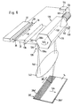
- a first simplest embodiment shown in FIGS. 1 and 2 a device according to the invention, as Whole designated 10, to generate an image 12 on an image area 14 - for example a projection area, on which the image is recognizable to a human eye is generated - includes a variety of in a row of lights 16 arranged along a longitudinal direction 18 of the row of lights 16
- Semiconductor emitters 20, each one of one common control 22 via individual control lines 24 are controllable.
- the longitudinal direction 18 extends transversely to an optical one Axis 26 of a projection optic designated as a whole by 28, which has an exit spot 30 of each semiconductor emitter 20, from which radiation 32 generated by the latter emerges, maps onto an image spot 34 of the image area 14, which of the radiation generated by the semiconductor emitter 20 is then illuminated.
- the projection optics 28 is constructed so that the exit spot 30 of each semiconductor emitter 20 only one at a time single image spot 34 is projected into the image area 14.
- the projection optics 28 a represents simple lens, arise on the image surface 14 in in a longitudinal direction 36 individual image spots lying next to one another 34, which together form a series of images 38.
- the projection optics 28 is designed so that the individual image spots 34 of the image row 38 in the direction of Do not overlap longitudinal direction 36. Is particularly preferred an embodiment of the projection plane, in which the Image spots 34 with their outer edges in a little follow or adjoin the distance.
- Fig. 12 human eye observing includes the control 22, as shown in Fig. 2, one for all semiconductor emitters 20 common power source 40, one for each Semiconductor emitter 20 provided current control block, which, for example, an FET transistor 44 as a current-controlling one Includes element at the gate as a storage element Capacitor 46 is connected. This capacitor 46 each Current control block 42 is connected via a control switch 48 of a certain charge, the charge in the capacitor 46 sets the current through the FET transistor 44.
- current control block which, for example, an FET transistor 44 as a current-controlling one Includes element at the gate as a storage element Capacitor 46 is connected.
- This capacitor 46 each Current control block 42 is connected via a control switch 48 of a certain charge, the charge in the capacitor 46 sets the current through the FET transistor 44.
- the charge to be stored in the capacitor 46 becomes from a buffer 50 for each capacitor 46 each Current control blocks 42 by triggering the drive switch 48 read from the buffer 50, preferably the buffer 50 stores all control parameters and by triggering the control switch 48 all control parameters simultaneously in the capacitors 46 of all current control blocks 42 can be read.
- a trigger block 52 is for triggering the control switch 48 intended.
- the intensity of the radiation 32 emitted by it can be determined at the activation time t 1 by appropriately charging the capacitor 46 of the corresponding control block 42. The charge is then retained in the capacitor 46 so that the intensity of the radiation from the semiconductor emitter remains constant until the next activation time t 2 . If the charge in the capacitor 46 is lowered at this point in time, this intensity is also maintained until the next triggering point in time t 3 .
- the maximum intensity and thus the maximum charge are stored in capacitor 46, while at activation time t 4 the minimum charge is stored, so that semiconductor emitter 20 does not emit any radiation or radiation with intensity 0 between activation time t 4 and t 5 sends out.
- each semiconductor emitter 20 has its own Control block 42 is provided, each individual semiconductor emitter can now 20 of the light row 16 individually controlled be, so that the image row 38 image spots 34 different Intensity.
- Controls 22 'shown in Fig. 4 are those Components that are identical to the controller 22 with provided the same reference numerals so that with respect to their Description on the explanations for the controller 22 in full Reference is made.
- each control block 42 ' only the control transistor 44, the gate of which by a Pulse shaper stage 60 is controlled and only is switched on and off between the states.
- the pulse shaper stage in turn saves the data at the respective activation time t transmitted control parameters and shapes accordingly the control parameters a control pulse different Length for the control transistor 44 after Principle of pulse width modulation, so that the semiconductor emitter 20 is either on or off, however with different lengths of time between the respective Driving times t, as shown in Fig. 5.
- the constant intensity values between the control points t1, t2, t3 and t4 are realized by pulse durations ⁇ t 1 , ⁇ t 2 , ⁇ t 3 of different lengths, the semiconductor emitter during the pulse durations ⁇ t 1 , ⁇ t 2 and ⁇ t 3, respectively, of radiation 32 with the maximum power.
- the human eye takes a temporal averaging when viewing the image spot 34 and thus the different pulse widths .DELTA.t 1 , .DELTA.t 2 and .DELTA.t 3 convey the impression in the human eye, as if the represented intensity values would be present during the entire period between the control times t 1 , t 2 , t 3 and t 4 .
- controller 22 is identical to the controller 22 built up.
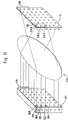
- a second embodiment shown in Fig. 6, includes the projection optics designated as a whole by 128 a polygon mirror 130 rotating about an axis 132 is driven by a drive 134.
- the polygon mirror 130 in turn has a plurality of equiangularly spaced polygon surfaces 136 arranged around the axis 132, one of the polygon surfaces 136 as a reflection surface serves.
- the light row 16 includes exactly as in the first embodiment a plurality in the longitudinal direction 18 in succession arranged semiconductor emitter 20, also are controlled by a controller 22 or 22 '.
- the radiation 32 emerging from the exit spots 30 becomes first by a first focusing optics 138 on the in Reflected polygon surface 136 focused, and that of the polygon surface 136 in the reflection position reflected radiation 140 is transmitted through a second focusing optics 142 intermediate focus and on the image surface 14 pictured.
- the polygonal surface is in the reflection position 136 while being illuminated by the radiation 32, does not arise on the image surface 14 only one row of images 38, but a multitude of Image rows 38 'which are in a direction perpendicular to the longitudinal direction 36 extending transverse direction 144 are arranged side by side.
- a first row of images 38a ' is then on the image surface 14 generated when the standing in the reflection position Polygon surface 136 with its foremost in the direction of rotation Area 136a is acted upon by the radiation 32, and the last image row 38b 'is generated when the in Polygon surface 136 with its in Direction of rotation 146 of the polygon mirror 130 rearmost area 136b is acted upon by the radiation 32.
- a Light beam 150 for example, that in the reflection position standing polygon area 136 opposite polygon area 136 illuminates, with the reflected radiation 152 hits a detector designated as a whole by 154, which one detector area 156 or more detector areas 156, the detector areas 156 being one Have an approximate cross-section of the reflected one Radiation corresponds to 152, so that when the reflected radiation 152 on the respective detector area 156 an exact angular position of the polygon mirror 130 is set.
- the first detector area 156 is positioned that when the reflected radiation strikes 152 the polygon surface 136 in the reflection position the exit spots 30 of the semiconductor emitter 20 of the Illuminates row 16 on the first row of images 38'a.
- the second detector surface 156 is preferably arranged such that when the reflected radiation 152 strikes it the polygon surface 136 standing in the reflection position Exit spots 30 of the semiconductor emitters 20 of the light row 16 maps to the second row of images 38 'and so on.
- the semiconductor emitters 20 can be switched off shortly before the respective activation time t simply by the maximum pulse width ⁇ t being shorter by the amount ⁇ t k than the period between successive activation times t, which preferably follow one another at constant time intervals.
- each single angular position of the reflection of the exit spots 30 corresponds to the light row 16 in one of the picture rows 38 'and thus the image rows 38 'are illuminated for a defined time and then in the reflection position standing polygon surface 136 in the next rotational position "jumps".
- edge 160 by rapid rotation of the polygon mirror 130 to jump away.
- the trigger block 52 can be controlled so that the detection the rotational position of the polygon mirror 130 by means of the detector 154 can be omitted.
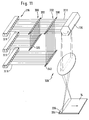
- a multi-colored image for a human eye - for example to create a television picture is with one third exemplary embodiment, shown schematically in FIG. 10, provided that each row of lights 216 three parallel to each other extending rows 218, 220 and 222 of semiconductor emitters 20, the row 218 of semiconductor emitters 20R is built, which emit red light, which Row 220 is made up of semiconductor emitters 20G which emit green light and the 222 series of semiconductor emitters 20B that emit blue light.
- the projection optics 228 are constructed so that each a semiconductor emitter 20R, a semiconductor emitter 20G, and a Semiconductor emitter 20B illuminate an image spot 234, wherein in the simplest case it is provided that each of the Semiconductor emitters 20R, 20G and 20B produced partial image spots 236B, 236G and 236R are not congruent, but not at all or only partially overlap.
- such Projection optics 228 for intermediate focusing of the radiation 32 onto the polygon mirror 130 by means of the first focusing optics 138 can be dispensed with.
- the focusing optics 228 are identical like the focusing optics 128 of the second exemplary embodiment, so that for details on this Reference is made.
- rows 218, 220 and 222 of the semiconductor emitters 20R, 20G and 20B analogous to that described in connection with the first embodiment Possibilities, however, for each of the rows 218, 220 and 222 a buffer 50 and for each Semiconductor emitter 20 requires a current control block 42 is; however, the control is such that at a Control time t the control parameters for the semiconductor emitter 20R, 20G and 20B of all three rows 218, 220 and 222 can be read from the buffer at the same time.
- FIG. 11 In a fourth embodiment shown in FIG. 11 are also the three rows 218, 220 and 222 the semiconductor emitters 20R, 20G and 20B, respectively. The same is controlled as in Described in connection with the third embodiment.
- the Projection optics 328 between the light row 216 and the Polygon mirror 130 two sets of mirrors 330 and 332, respectively the radiation 32R of the semiconductor emitter 20R, the radiation 32G the semiconductor emitter 20G and the radiation 32B the semiconductor emitter 20B to unite with each other.
- the first set of mirrors 330 includes one in the beam path of FIG Radiation 32R arranged dichroic mirrors 333 and the radiation 32G onto the dichroic mirror 333 reflective mirror 335.
- the second set of mirrors 332 includes one arranged in the beam path of the radiation 32R dichroic mirror 338 and radiation 32B mirror 340 reflecting dichroic mirror 338.
- a fifth embodiment shown in Fig. 12, are a plurality of light rows 416 of semiconductor emitters 20 arranged in a two-dimensional matrix 420, and the Projection optics 428 is constructed to accommodate everyone Exit spot of each semiconductor emitter 20 as an image spot 34 images on the image surface 14, so that the Luminous rows 416 with adjacent exit spots 30 of the semiconductor emitters 20 image rows 438 with adjacent ones Image spots correspond, each image spot 34 an exit spot 30 of the corresponding semiconductor emitter 20 corresponds.
- the imaging optics 428 is preferred a lens optics, the exit spots via an intermediate focus F. 30 of the semiconductor emitter 20 as enlarged Image spots 34 on the image surface 14.
- the radiation 32 of the same wavelength emit is therefore with appropriate control a single color two-dimensional image is formed through the image spots 34 of the image rows 438 on the image surface 14 representable.
- All semiconductor emitters can be used for image generation To let 20 of the matrix 420 shine at the same time, for each semiconductor emitter 20 a control block 42 or 42 'is to be provided. With changing image information can also the control parameters for the respective current control block 42 or 42 'can be changed.
- the matrix 521 is constructed from semiconductor emitters that each light row 516 three rows 518, 520 and 522 of Has semiconductor emitters 20R, 20G and 20B, each Generate radiation of different wavelengths, for example Red, green and blue, so that the three rows 518, 520 and 522 of monochrome semiconductor emitters 20R, 20G and 20B after their projection by means of the projection optics 428 Generate image spots 534 on the image area, their partial image spots 536R, 536G and 536B one for human Eye colored image impression due to their short distance convey, with sub-image patches 536R, 536G and 536B lie next to each other or only partially overlap.
- the Image spots 534 thus also form image rows 538.
- the matrix 521 now comprises a plurality of ones arranged one above the other such light rows 516, so that when using the same Projection optics 428 also have a plurality of one above the other arranged and a two-dimensional image 12th resulting series 538 arises.
- the three are each an image spot 534 illuminating semiconductor emitters 20R, 20G and 20B, respectively control simultaneously to the desired color mixture in the To be able to generate image spot 534.
- a seventh embodiment 14 the rows 518 of semiconductor emitters 20R to form a matrix 620R which Rows 520 of semiconductor emitters 20G to a matrix 620G and the rows 522 of semiconductor emitters 20B into a matrix 620B.
- the radiation 32R of the entirety of the semiconductor emitters the Matrix 620R is now replaced by a mirror set 630 with the Radiation 32G of the 620G matrix combined in that 32R radiation beam path a dichroic mirror 632 is arranged on which a mirror 634 the radiation 32G of the Matrix 620G reflected.
- a Mirror set 636 provided which is a dichroic Mirror 638 also in the beam path of radiation 32R on which a reflection mirror 640 the radiation 32B of the matrix 620B reflected, so that the total radiation 32V combined all three radiations 32R, 32G and 32B, the mirror sets 630 and 636 are to be designed such that the radiations 32R, 32G and 32B correspond to each other Semiconductor emitter 20R, 20G and 20B have an image spot either by overlapping or by closely located partial image spots illuminate and thus an overall color impression convey.
- the projection optics are in the seventh embodiment trained in the same way as the fifth and sixth embodiments, so that this full reference can be made.
- the device according to the invention comprise the semiconductor emitter as radiation sources, preferably as so-called edge emitters trained semiconductor laser, as shown in Fig. 15 schematically shown.
- Such edge emitters consist of a Plurality of semiconductor layers 800, between which one laser-active layer 802 is arranged. For this laser active Layer occurs in the area of an exit spot 804 the laser radiation 806.
- Such an edge emitter is operated by supplying current via two power connections 808 and 810, the current in flows substantially perpendicular to layers 800 and 802.
- Embodiments of such edge emitters are in the Laser Focus World Magazine, July 1993, Vol. 29, No. 7, Pages 83 to 92 described in detail.
- edge emitter can be seen in the fact that these are lined up in a simple manner as so-called Array can be made on a substrate.
- edge emitters it is possible to as radiation sources semiconductor lasers in the form of so-called 16 to provide vertical emitters, wherein with such vertical emitters also a laser active one Layer 902 between a plurality of semiconductor layers 900 is provided and on both sides of the laser-active layer 902 additional layers 904 serving as Bragg reflectors are provided.
- the resulting one spreads Laser radiation not parallel to the edge emitter as with the active layer 802, but perpendicular to the active one Layer 902 penetrates substrate 910 and preferably occurs in the process perpendicular to the plane of the substrate 910.
- the following laser materials are preferably used as laser materials for the generation of radiation in the visible range with different colors: Al x Ga y In 1-xy P on GaAs for 610-690 nm red Zn 1-x Mg x S 1-y Se y on GaAs for 450-550 nm blue green Al x Ga y In 1-xy N For UV - red
- Such materials would be, for example Al x Ga 1-x As on GaAs (780-880 nm) for blue In x Ga 1-x As on GaAs (880-1100 nm) for blue, green In 1-x Ga x As y P 1-y on InP (1100-1600 nm) for red.
- the wavelength of the Radiation from the semiconductor emitter doubling the radiation source, 17 and 18 as a whole designated 820 comprises an array 822 of on a common substrate 824 arranged edge emitters 826, which by special on the common substrate 824 arranged laser active layers are formed and in each case as a laser-active layer 802 striped area 828 one on the common Have substrate 824 arranged continuous layer 830.
- Each of the semiconductor lasers 826 serving as a radiation source a frequency doubler 832 is assigned to each each comprises a waveguide structure 834, in which a frequency-doubled medium arranged as a waveguide core 836 is.
- the waveguide structure 834 guides the radiation generated by the respective semiconductor laser 826 in such a narrow cross section that a power density of at least 10 5 W / cm 2 , preferably at least 10 6 W / cm 2 , is required for efficient frequency doubling in the frequency doubling medium is achieved.
- FIGS. 17 and 18 are all frequency doublers 832 also on a common Substrate 838 arranged in the form of an array 840.
- the waveguide structure 834 is formed by a Base layer 842 and a cover layer 844, which upper and represent lower walls of the waveguide channel 834, and in Strip regions 846 and 848 spaced apart from one another an intermediate layer 850 which has side walls of the waveguide channel 834 and form a strip region 852 of the Include intermediate layer 850 between them, which is the Frequency doubling medium 836 serving as a waveguide core forms.
- the base layer 842, the cover layer 844 and the strip-shaped Regions 846 and 848 of the intermediate layer 850 have a refractive index that is less than the refractive index of the strip-shaped region 852, so that at the Limits between the striped area 852 and the Layers 842 and 844 as well as the stripe-shaped areas 846 and 848 a total reflection of the radiation and thus the Guiding the radiation in the waveguide structure 834 he follows.
- the semiconductor emitter is preferably constructed such that to the array 822 of semiconductor lasers 826, the array 840 of Frequency doubler 832 immediately connects, so that the Radiation from the laser active layers 828 immediately in crosses the waveguide channels 834.
- the expanse of the waveguide structures is expedient 834 approximately to their longitudinal direction 854 chosen the same size as the extent of the laser active Areas 828 transverse to the direction of propagation 856 of the laser radiation.
- the fundamental wave the is called the one coming from the corresponding semiconductor laser 826 Radiation, and the frequency-doubled radiation during the all the way through the frequency doubling medium in phase stay. This is optimally achieved when using a non-critical or non-critical phase adjustment worked at which the angle is 0 or 90 °.
- An adjustment to the corresponding wavelength takes place at the respective Material preferably by varying the temperature, so that, for example, the substrate 838 on a Temperature control device 860 sits, with which the entire array 840 from frequency doublers 832 to one for the uncritical Phase adjustment optimal temperature can be brought and on this is durable.
- the temperature control device 860 is preferably with a Provide control over which a predeterminable temperature adjusted and maintained by readjustment can.
- the crystal direction is expediently in the frequency doubling Medium 836 by the alignment of the substrate 838, which is oriented so that the optical Axes of the substrate in the desired direction to the longitudinal direction 854 of the waveguide channel 834 are aligned. If layers 842, 844 and 8 are left on this substrate 838 850 made of the same base material, possibly with different ones Endowments, growing up, so they have Layers have the same alignment of the optical axes as the substrate 838 and thus the location of the Optical axes can be specified in the frequency-doubling medium 836.
- a variant 840 'of the array 840 of frequency doublers 832, shown in Fig. 19, is not associated with a uncritical phase adjustment worked, but the phase adjustment is achieved in that in the frequency doubling Medium 836 'domains 870 and 872 follow each other, in which the nonlinear coefficients of the frequency doubling Medium 836 have opposite signs.
- An extension L of the domains 870 and 872 in the longitudinal direction 854 of the waveguide channels 834 is to be coordinated that it corresponds to the coherence length.
- a crystal as a frequency-doubling medium Lithium niobate for the wavelengths green and red is used and for the blue wavelength a crystal of potassium niobate.
- the waveguide structure 834 is produced in that the material surrounding the waveguide core is lithium niobate or Potassium niobate is that, in addition to magnesium or others Refractive index-lowering elements was doped.
- an inventive Semiconductor emitters shown in Fig. 20 and as a whole Designated 920, finds an array 922 as a vertical emitter trained semiconductor lasers 926 use.
- the radiation 928 this semiconductor emitter is made by focusing Elements 930 focused on frequency doublers 932, which also arranged in an array 940 on a common substrate and are designed and constructed in the same way as the array 840, so that the explanations for this are fully Can be referenced.
- the focusing one Optics 930 are not designed as lens optics, but as gradient index lenses, which act as a block between the respective semiconductor lasers 926 and the corresponding ones Frequency doublers 932 are used and due to the Gradient index the radiation 928 onto the waveguide channels Focus 934.
- the frequency doubler is preferably at the end 932 expansion optics 970 arranged, which also Gradient index lenses are essentially one generate parallel beam 972.
Landscapes
- Physics & Mathematics (AREA)
- Optics & Photonics (AREA)
- Engineering & Computer Science (AREA)
- Multimedia (AREA)
- Signal Processing (AREA)
- General Physics & Mathematics (AREA)
- Mechanical Optical Scanning Systems (AREA)
- Devices For Indicating Variable Information By Combining Individual Elements (AREA)
- Semiconductor Lasers (AREA)
- Projection Apparatus (AREA)
Claims (51)
- Dispositif pour produire une image visible pour l'oeil humain, sur une surface image (14), comprenantcaractérisé en ce qu'on utilise des lasers à semiconducteurs comme émetteurs à semiconducteurs,une rampe lumineuse (16), qui possède une multiplicité d'émetteurs à semiconducteurs (20), dont chacun produit un rayonnement (32R, 32G, 32B) possédant l'une de trois longueurs d'onde différentes (R, G, B), avec lesquelles une lumière blanche peut être produite par mélange des couleurs,un système optique de projection (228, 328, 428), qui forme l'image des spots de sortie (30) des émetteurs à semiconducteurs (20),que le système optique de projection (228, 328, 428) éclaire des zones d'image (234, 334, 534) dans la surface image (14) visible pour l'oeil humain,que chacune des zones d'image (234, 334, 534) comprend trois zones d'image partielles non congruentes (236R, 236G, 236B; 336; 536R, 536G, 536B), dont il est possible d'éclairer chacune par un rayonnement (32R, 32G, 32B) avec l'une de trois longueurs d'onde différentes (R, G, B) au point de pouvoir produire pour l'oeil humain l'impression de couleurs mixtes dans la zone d'image (234, 334, 534), etque le système optique de projection (228, 328, 428) associe à chacun des trois zones d'image partielles (236R, 236G, 236B; 336; 536R, 536G, 536B) l'un de respectivement trois émetteurs à semi-conducteurs (20R, 20G, 20B) produisant des rayonnements (32R, 32G, 32B) possédant les trois longueurs d'onde différentes (R, G, B).
- Dispositif selon l'une des revendications précédentes, caractérisé en ce que la multiplicité des émetteurs à semiconducteurs (20) est si grande qu'un spot de sortie (30) d'un émetteur à semiconducteurs (20) est associé exclusivement, à un instant, à une zone d'image (34) de la série d'images (38).
- Dispositif selon l'une des revendications précédentes, caractérisé en ce que les émetteurs à semiconducteurs (20) émettent le rayonnement (32) dans le temps entre deux instants successifs de commande (t1, t2, ...).
- Dispositif selon la revendication 3, caractérisé en ce que les instants de commande (t1, t2, ...) se succèdent à des intervalles constants.
- Dispositif selon la revendication 3 ou 4, caractérisé en ce que les émetteurs à semiconducteurs (20) émettent le rayonnement (32) avec une intensité réglable de façon variable.
- Dispositif selon la revendication 5, caractérisé en ce que les émetteurs à semiconducteurs (20) émettent le rayonnement (32) avec l'intensité réglée d'une manière essentiellement constante entre deux instants de commande (t1, t2, ...).
- Dispositif selon la revendication 5 ou 6, caractérisé en ce que le réglage de l'intensité de rayonnement (32) de chaque émetteur à semiconducteurs (20) s'effectue à chaque instant de commande (t1, t2, ...).
- Dispositif selon l'une des revendications 1 à 4, caractérisé en ce que les émetteurs à semiconducteurs (20) émettent, entre les instants de commande (t1, t2, ...), soit un rayonnement (32) ayant l'intensité maximale mais avec une durée réglable d'une manière variable (Δt1, Δt2, ...), soit n'émettent aucun rayonnement.
- Dispositif selon la revendication 8, caractérisé en ce que le réglage d'une intensité moyenne perçue par un observateur est effectué par modification de la durée (Δt1, Δt2, ...) de l'émission du rayonnement (32).
- Dispositif selon la revendication 8 ou 9, caractérisé en ce que le réglage de la durée (Δt1, Δt2, ...) de l'émission du rayonnement (32) s'effectue à chaque instant de commande (t1, t2, ...).
- Dispositif selon l'une des revendications précédentes, caractérisé en ce que les trois émetteurs à semiconducteurs (20R, 20G, 20B), qui éclairent chacun une zone d'image (34), peuvent être commandés simultanément.
- Dispositif selon l'une des revendications précédentes, caractérisé en ce que la rampe lumineuse (16) possède au moins une série d'émetteurs à semiconducteurs (20), qui émettent un rayonnement possédant la même longueur d'onde.
- Dispositif selon la revendication 12, caractérisé en ce que pour l'éclairement des zones d'image (34) d'une rangée d'images (38), la rampe lumineuse correspondante (16) comporte trois rangées (218, 220, 222; 518, 520, 522), parallèles entre elles, d'émetteurs à semiconducteurs (20R, 20G, 20B), et les émetteurs à semiconducteurs (20R, 20G, 20B) de chaque rangée émettant sensiblement la même longueur d'onde.
- Dispositif selon l'une des revendications précédentes, caractérisé en ce que parmi les émetteurs à semiconducteurs (20) d'une rampe lumineuse (16), au moins les émetteurs, qui sont associés à un dixième des zones d'image (34) d'une série d'images (38), peuvent être commandés au même instant de commande.
- Dispositif selon la revendication 14, caractérisé en ce que les émetteurs à semiconducteurs (20) d'une rampe lumineuse (16) associés à toutes les zones d'image (34) d'une série d'images (38) peuvent être commandés simultanément.
- Dispositif selon l'une des revendications précédentes, caractérisé en ce que pour la commande simultanée de plusieurs émetteurs à semiconducteurs (20), il est prévu une mémoire intermédiaire (50), dans laquelle les paramètres de commande peuvent être lus en parallèle pour la commande simultanée de la pluralité d'émetteurs à semiconducteurs (20).
- Dispositif selon la revendication 16, caractérisé en ce que la mémoire intermédiaire (50) reçoit entre les instants de commande (t1, t2, ...) les paramètres de commande pour les émetteurs à semiconducteurs (20).
- Dispositif selon la revendication 17, caractérisé en ce que les paramètres de commande peuvent être lus en série dans la mémoire intermédiaire (50).
- Dispositif selon l'une des revendications 16 à 18, caractérisé en ce que les paramètres de commande peuvent être produits par un générateur d'images (34).
- Dispositif selon la revendication 19, caractérisé en ce que le générateur d'images (54) produit en série les paramètres de commande.
- Dispositif selon l'une des revendications précédentes, caractérisé en ce qu'à chaque émetteur à semiconducteurs (20) est associée une unité de commande (42, 60), qui mémorise le paramètre de commande depuis un instant de commande (t1) jusqu'à l'instant de commande suivant (t2).
- Dispositif selon l'une des revendications précédentes, caractérisé en ce que le système optique de projection (28, 128, 228) forme une image d'une rampe lumineuse (16) successivement sur plusieurs rangées d'images (38a, ..., 38b).
- Dispositif selon la revendication 22, caractérisé en ce que le système optique de projection (28, 128, 228) comprend un élément (130) déviant le rayonnement, qui forme une image de la rampe lumineuse (16) sur des rangées successives d'images (38).
- Dispositif selon la revendication 23, caractérisé en ce que l'élément déviant le rayonnement est un élément réfléchissant mobile (130).
- Dispositif selon la revendication 24, caractérisé en ce que l'élément réfléchissant (130) est déplaçable dans des positions angulaires définies, qui forment l'image de la rampe lumineuse (16) respectivement dans l'une des rangées d'images (38).
- Dispositif selon l'une des revendications 23 à 25, caractérisé en ce que l'élément déviant le rayonnement est formé par un miroir polygonal rotatif (130).
- Dispositif selon la revendication 26, caractérisé en ce que le miroir polygonal (130) tourne avec une vitesse de rotation constante.
- Dispositif selon la revendication 27, caractérisé en ce que le miroir polygonal (130) traverse, avec chaque facette (136) de la surface polygonale, le nombre des rangées d'images (38) sous l'effet d'une rotation sur une plage angulaire déterminée, puis passe à la facette immédiatement suivante (136) de la surface polygonale.
- Dispositif selon l'une des revendications 23 à 28, caractérisé en ce que le système optique de projection (28) focalise le rayonnement des émetteurs à semi-conducteurs (20) de la rampe lumineuse (16) essentiellement sur l'élément (130) déviant le rayonnement.
- Dispositif selon l'une des revendications 1 à 21, caractérisé en ce qu'une rampe lumineuse (16) est associée à chaque rangée d'images (38).
- Dispositif selon la revendication 30, caractérisé en ce que le système optique de projection (428, 628) forme l'image de la multiplicité de rampes lumineuses (16) dans la multiplicité de rangées d'images (38).
- Dispositif selon l'une des revendications précédentes, caractérisé en ce que le système optique de projection (28, 128, 228, 328, 428, 628) produit des zones d'image (34) séparées par de faibles distances.
- Dispositif selon la revendication 32, caractérisé en ce que les zones d'image (34) se jouxtent entre elles pour l'essentiel.
- Dispositif selon l'une des revendications précédentes, caractérisé en ce que le système optique de projection (228, 328) réunit les rayonnements (32R, 32G, 32B) des trois émetteurs à semi-conducteurs (20R, 20G, 20B), qui émettent avec des longueurs d'onde différentes, pour former un faisceau de rayonnement (32V).
- Dispositif selon l'une des revendications précédentes, caractérisé en ce que chaque émetteur à semiconducteurs (820, 920) comprend une source de rayonnement à semiconducteurs (826, 926) et un doubleur de fréquence (832, 932) pour le rayonnement émis par la source de rayonnement à semiconducteurs.
- Dispositif selon la revendication 35, caractérisé en ce que le doubleur de fréquence (832, 932) comprend une structure à guide d'ondes (834, 934), qui guide le rayonnement de chaque source de rayonnement (826, 926) avec une densité de puissance égale à au moins 105 W/cm2, d'une manière comprimée, et un milieu (836, 936) qui double la fréquence et est disposé dans la structure à guide d'ondes (834, 934).
- Dispositif selon la revendication 35 ou 36, caractérisé en ce que les doubleurs de fréquence (832) se raccordent directement aux sources de rayonnement (826).
- Dispositif selon la revendication 35 ou 36, caractérisé en ce qu'entre chaque source de rayonnement (926) et chaque doubleur de fréquence (932) est disposé un système optique (930) qui focalise le rayonnement dans la structure à guide d'ondes (934).
- Dispositif selon l'une des revendications 35 à 38, caractérisé en ce que les sources de rayonnement (826, 926) d'une rampe lumineuse (16) sont disposées suivant une rangée et que les doubleurs de fréquence (832, 932) de la rampe lumineuse (16) sont disposés, du côté d'une sortie des sources de rayonnement (826, 926), également suivant une rangée.
- Dispositif selon l'une des revendications 35 à 39, caractérisé en ce que plusieurs des sources de rayonnement (826) sont disposées sur un substrat commun (834).
- Dispositif selon l'une des revendications 35 à 40, caractérisé en ce que plusieurs des doubleurs de fréquence (832, 932) sont disposés sur un substrat commun (838).
- Dispositif selon l'une des revendications 35 à 41, caractérisé en ce que chaque structure à guide d'ondes (834, 934) de chaque doubleur de fréquence (832, 932) est un guide d'ondes "monomode".
- Dispositif selon l'une des revendications 35 à 42, caractérisé en ce que chaque structure à guide d'ondes (834, 934) est formée par un matériau de paroi qui entoure le milieu (836, 936) qui double la fréquence et forme le coeur du guide d'ondes, et possède un indice de réfraction inférieur à celui du coeur du guide d'ondes.
- Dispositif selon la revendication 43, caractérisé en ce que le matériau de paroi est monté sur le même matériau que le milieu (836, 936) qui double la fréquence et possède, sur la base d'un dopage différent, un indice de réfraction inférieur à celui de ce milieu.
- Dispositif selon la revendication 43 ou 44, caractérisé en ce que la structure à guide d'ondes (834, 934) est formée par dopage de zones formant le matériau de paroi, avec un matériau identique à celui du milieu réalisant un doublement de la fréquence.
- Dispositif selon l'une des revendications 35 à 45, caractérisé en ce que la structure à guide d'ondes (834, 934) est constituée par des couches (842, 844, 850) déposées sur un substrat (838, 938) et entourant le matériau de paroi.
- Dispositif selon l'une des revendications 35 à 46, caractérisé en ce que le milieu (836, 936) qui double la fréquence est formé par une couche (850) déposée sur un substrat (838, 938).
- Dispositif selon la revendication 47, caractérisé en ce qu'une orientation définie d'axes optiques du milieu (836, 936) qui double la fréquence est prédéterminée par l'orientation du substrat (838, 938).
- Dispositif selon l'une des revendications 36 à 38, caractérisé en ce que le milieu (836, 936) qui double la fréquence est agencé, et ses axes optiques sont orientés par rapport au canal des guides d'ondes, de telle sorte qu'une adaptation de phase non critique s'effectue entre le rayonnement et le rayonnement dont la fréquence est doublée, dans la direction longitudinale (834, 954) de la structure à guide d'ondes (834, 934).
- Dispositif selon la revendication 49, caractérisé en ce que le milieu (836, 936) qui double la fréquence peut être amené à une température définie.
- Dispositif selon l'une des revendications 36 à 48, caractérisé en ce que le milieu (836') qui double la fréquence est agencé et orienté de telle sorte qu'il se produit quasiment une adaptation de phase dans la direction longitudinale (854) de la structure à guide d'ondes (834).
Applications Claiming Priority (2)
| Application Number | Priority Date | Filing Date | Title |
|---|---|---|---|
| DE4413829 | 1994-04-20 | ||
| DE4413829A DE4413829A1 (de) | 1994-04-20 | 1994-04-20 | Vorrichtung zur Erzeugung eines Bildes |
Publications (3)
| Publication Number | Publication Date |
|---|---|
| EP0683595A2 EP0683595A2 (fr) | 1995-11-22 |
| EP0683595A3 EP0683595A3 (fr) | 1996-07-03 |
| EP0683595B1 true EP0683595B1 (fr) | 2001-12-05 |
Family
ID=6516015
Family Applications (1)
| Application Number | Title | Priority Date | Filing Date |
|---|---|---|---|
| EP95105829A Expired - Lifetime EP0683595B1 (fr) | 1994-04-20 | 1995-04-19 | Dispositif de formation d'image |
Country Status (4)
| Country | Link |
|---|---|
| US (1) | US5874929A (fr) |
| EP (1) | EP0683595B1 (fr) |
| JP (1) | JP3107501B2 (fr) |
| DE (2) | DE4413829A1 (fr) |
Families Citing this family (30)
| Publication number | Priority date | Publication date | Assignee | Title |
|---|---|---|---|---|
| US6175440B1 (en) * | 1994-02-02 | 2001-01-16 | Advanced Laser Technologies, Inc. | Laser beam display |
| DE19546039A1 (de) * | 1995-12-09 | 1997-06-12 | Forsch Mineralische Und Metall | Bildschirm, Verfahren zu seiner Herstellung sowie Verfahren und Vorrichtung zur Darstellung von Bildern auf einem Bildschirm |
| US5973727A (en) * | 1997-05-13 | 1999-10-26 | New Light Industries, Ltd. | Video image viewing device and method |
| US6067059A (en) * | 1998-02-04 | 2000-05-23 | Quarton, Inc. | Laser dot matrix display systems |
| DE19818007A1 (de) * | 1998-04-22 | 1999-10-28 | Deutsch Zentr Luft & Raumfahrt | Einrichtung zur Erzeugung eines Bildes |
| JP2000089148A (ja) * | 1998-07-13 | 2000-03-31 | Canon Inc | 光走査装置及びそれを用いた画像形成装置 |
| DE19840928A1 (de) * | 1998-09-08 | 2000-03-09 | Heidelberger Druckmasch Ag | Multibeam Laser Scanner |
| DE19963805B4 (de) | 1999-12-30 | 2005-01-27 | Osram Opto Semiconductors Gmbh | Weißlichtquelle auf der Basis nichtlinear-optischer Prozesse |
| US6351324B1 (en) * | 2000-03-09 | 2002-02-26 | Photera Technologies, Inc. | Laser imaging system with progressive multi-beam scan architecture |
| JP2001265275A (ja) * | 2000-03-16 | 2001-09-28 | Olympus Optical Co Ltd | 画像表示装置 |
| US7102700B1 (en) * | 2000-09-02 | 2006-09-05 | Magic Lantern Llc | Laser projection system |
| CN1484818A (zh) | 2000-10-27 | 2004-03-24 | 具有交错光束扫描的光束显示器 | |
| TWI233500B (en) * | 2001-04-23 | 2005-06-01 | Reveo Inc | Image display system and electrically actuatable image combiner therefor |
| TW472225B (en) * | 2001-06-08 | 2002-01-11 | Shiu-Hua Huang | Sequential type projection apparatus |
| US20030199260A1 (en) * | 2002-04-19 | 2003-10-23 | Casey Francis M. | Wireless communication receiver and method for determining a reference frequency in a wireless communication device |
| US7184104B2 (en) * | 2002-05-03 | 2007-02-27 | Hewlett-Packard Development Company, L.P. | Projector having scanning optics |
| US7230657B2 (en) * | 2002-05-03 | 2007-06-12 | Hewlett-Packard Development Company, L.P. | Light emitting device projection methods and systems |
| US7167216B2 (en) * | 2002-05-03 | 2007-01-23 | Hewlett-Packard Development Company, L.P. | Projection system with adjustable aspect ratio optics |
| DE10242142A1 (de) * | 2002-09-03 | 2004-03-25 | Kleo Halbleitertechnik Gmbh & Co Kg | Verfahren und Vorrichtung zum Herstellen von belichteten Strukturen |
| US7258448B2 (en) * | 2004-03-25 | 2007-08-21 | Calsonic Kansei Corporation | Display device |
| DE102006008080A1 (de) * | 2006-02-22 | 2007-08-30 | Kleo Maschinenbau Ag | Belichtungsanlage |
| DE102006059818B4 (de) * | 2006-12-11 | 2017-09-14 | Kleo Ag | Belichtungsanlage |
| US8150267B1 (en) * | 2007-04-18 | 2012-04-03 | Hewlett-Packard Development Company, L.P. | Optical interconnect |
| DE102007019017A1 (de) * | 2007-04-19 | 2009-01-22 | Ldt Laser Display Technology Gmbh | Verfahren und Vorrichtung zum Projizieren eines Bildes auf eine Projektionsfläche |
| WO2009067678A2 (fr) * | 2007-11-24 | 2009-05-28 | Display Photonics, Inc. | Système de projection à base de panneau d'affichage à auto-émission |
| DE102009032210B4 (de) | 2009-07-03 | 2011-06-09 | Kleo Ag | Bearbeitungsanlage |
| JP2013503370A (ja) * | 2009-08-31 | 2013-01-31 | スリーエム イノベイティブ プロパティズ カンパニー | プロジェクション及びディスプレイシステム |
| DE102009046809B4 (de) * | 2009-11-18 | 2019-11-21 | Kleo Ag | Belichtungsanlage |
| JP5702216B2 (ja) * | 2011-04-22 | 2015-04-15 | 株式会社小糸製作所 | 光学ユニット |
| US20150124231A1 (en) * | 2012-06-01 | 2015-05-07 | Asml Netherlands B.V. | Assembly For Modifying Properties Of A Plurality Of Radiation Beams, A Lithography Apparatus, A Method Of Modifying Properties Of A Plurality Of Radiation Beams And A Device Manufacturing Method |
Family Cites Families (16)
| Publication number | Priority date | Publication date | Assignee | Title |
|---|---|---|---|---|
| JPS569763A (en) * | 1979-07-06 | 1981-01-31 | Canon Inc | Beam recording device |
| JPS5833753A (ja) * | 1981-08-24 | 1983-02-28 | Fujitsu Ltd | 除算器 |
| DE3529571A1 (de) * | 1985-08-17 | 1987-02-19 | Telefunken Electronic Gmbh | Verfahren zur periodischen ansteuerung von mehreren strahlungsaussendenden elementen und schaltungsanordnung zur durchfuehrung des verfahrens |
| JP2567479B2 (ja) * | 1988-10-17 | 1996-12-25 | 富士写真フイルム株式会社 | バーコードプリント装置 |
| JPH0425290A (ja) * | 1990-05-21 | 1992-01-29 | Victor Co Of Japan Ltd | 表示装置 |
| EP0458270B1 (fr) * | 1990-05-21 | 1996-11-27 | Victor Company Of Japan, Limited | Dispositif d'affichage |
| US5143577A (en) * | 1991-02-08 | 1992-09-01 | Hoechst Celanese Corporation | Smooth-wall polymeric channel and rib waveguides exhibiting low optical loss |
| US5229691A (en) * | 1991-02-25 | 1993-07-20 | Panocorp Display Systems | Electronic fluorescent display |
| US5294944A (en) * | 1991-03-06 | 1994-03-15 | Ricoh Company, Ltd. | Color image forming apparatus having means for properly superimposing image colors on each other |
| US5418546A (en) * | 1991-08-20 | 1995-05-23 | Mitsubishi Denki Kabushiki Kaisha | Visual display system and exposure control apparatus |
| EP0587228B1 (fr) * | 1992-09-07 | 1998-11-04 | Koninklijke Philips Electronics N.V. | Composant optique et élément optoélectronique pour l'augmentation de la fréquence d'un rayonnement électromagnétique |
| US5596339A (en) * | 1992-10-22 | 1997-01-21 | University Of Washington | Virtual retinal display with fiber optic point source |
| US5321718A (en) * | 1993-01-28 | 1994-06-14 | Sdl, Inc. | Frequency converted laser diode and lens system therefor |
| CN1119482A (zh) * | 1993-02-03 | 1996-03-27 | 尼托公司 | 图像投影的方法和设备 |
| US5534950A (en) * | 1993-10-04 | 1996-07-09 | Laser Power Corporation | High resolution image projection system and method employing lasers |
| US5513196A (en) * | 1995-02-14 | 1996-04-30 | Deacon Research | Optical source with mode reshaping |
-
1994
- 1994-04-20 DE DE4413829A patent/DE4413829A1/de not_active Ceased
-
1995
- 1995-04-19 DE DE59509895T patent/DE59509895D1/de not_active Expired - Fee Related
- 1995-04-19 EP EP95105829A patent/EP0683595B1/fr not_active Expired - Lifetime
- 1995-04-19 US US08/425,123 patent/US5874929A/en not_active Expired - Fee Related
- 1995-04-20 JP JP07095618A patent/JP3107501B2/ja not_active Expired - Fee Related
Also Published As
| Publication number | Publication date |
|---|---|
| EP0683595A3 (fr) | 1996-07-03 |
| JP3107501B2 (ja) | 2000-11-13 |
| US5874929A (en) | 1999-02-23 |
| EP0683595A2 (fr) | 1995-11-22 |
| DE4413829A1 (de) | 1995-10-26 |
| JPH08166770A (ja) | 1996-06-25 |
| DE59509895D1 (de) | 2002-01-17 |
Similar Documents
| Publication | Publication Date | Title |
|---|---|---|
| EP0683595B1 (fr) | Dispositif de formation d'image | |
| EP0696875B1 (fr) | Dispositif pour produire une image | |
| DE3882691T2 (de) | Video-abbildungssysteme. | |
| DE69519220T2 (de) | Einzeltafel-farbbildprojektionssystem mit verbesserter abtastung | |
| DE69123288T2 (de) | Anzeigegerät | |
| DE69329992T2 (de) | Farbbildprojektor | |
| DE69019055T2 (de) | Apparat für ein digitalisiertes Videosystem. | |
| DE69725582T2 (de) | Zeilensprung-farbbildprojektor | |
| DE19902110C2 (de) | Videoprojektionssystem zur Projektion von mehreren Einzelbildern | |
| DE60125183T2 (de) | Bildanzeigevorrichtung des projektionstyps | |
| DE69130665T2 (de) | Verfahren für die Wiedergabe von Bildern, erzeugt durch die Energie-Übertragung eines räumlichen Modulators | |
| DE69516802T2 (de) | Beleuchtungsystem für farbbildprojektion | |
| DE2539651C2 (de) | Anordnung zur Projektion von fernübertragenen Farbbildern | |
| DE19751106A1 (de) | Laserdrucker zum Drucken auf ein lichtempfindliches Medium | |
| DE112009001320T5 (de) | Strahlabtastung auf der Grundlage eines zweidimensionalen Polygonscanners zur Anzeige und für andere Anwendungen | |
| DE102013226622A1 (de) | Leuchtvorrichtung mit Leuchtstofffläche | |
| EP2049937A1 (fr) | Module de projection d'image | |
| DE69328906T2 (de) | Verfahren und gerät zum erzeugen von dreidimensionalen bildern | |
| DE19626096C1 (de) | Verfahren zur dreidimensionalen Bilddarstellung auf einer Großbildprojektionsfläche mittels eines Laser-Projektors | |
| DE10030417A1 (de) | Bildprojektor | |
| DE69324551T2 (de) | Sequentielle Lichtventil-Farbanzeigevorrichtung | |
| DE1462404C3 (de) | Vorrichtung zur Wiedergabe eines mehrfarbigen Fernsehbildes | |
| WO2000011513A1 (fr) | Dispositif permettant l'affichage volumetrique d'une image 3d par generation de plasma pulse en atmosphere naturelle au moyen d'un faisceau laser focalise | |
| DE2724921C2 (de) | Videobilddarstellungsgerät | |
| DE102012011202A1 (de) | Projektor und Verfahren zum Erzeugen eines Bildes |
Legal Events
| Date | Code | Title | Description |
|---|---|---|---|
| PUAI | Public reference made under article 153(3) epc to a published international application that has entered the european phase |
Free format text: ORIGINAL CODE: 0009012 |
|
| AK | Designated contracting states |
Kind code of ref document: A2 Designated state(s): DE FR NL |
|
| PUAL | Search report despatched |
Free format text: ORIGINAL CODE: 0009013 |
|
| AK | Designated contracting states |
Kind code of ref document: A3 Designated state(s): DE FR NL |
|
| 17P | Request for examination filed |
Effective date: 19961211 |
|
| RAP1 | Party data changed (applicant data changed or rights of an application transferred) |
Owner name: DEUTSCHES ZENTRUM FUER LUFT- UND RAUMFAHRT E.V. |
|
| RAP3 | Party data changed (applicant data changed or rights of an application transferred) |
Owner name: DEUTSCHES ZENTRUM FUER LUFT- UND RAUMFAHRT E.V. |
|
| 17Q | First examination report despatched |
Effective date: 19990426 |
|
| GRAG | Despatch of communication of intention to grant |
Free format text: ORIGINAL CODE: EPIDOS AGRA |
|
| GRAG | Despatch of communication of intention to grant |
Free format text: ORIGINAL CODE: EPIDOS AGRA |
|
| GRAH | Despatch of communication of intention to grant a patent |
Free format text: ORIGINAL CODE: EPIDOS IGRA |
|
| GRAH | Despatch of communication of intention to grant a patent |
Free format text: ORIGINAL CODE: EPIDOS IGRA |
|
| GRAA | (expected) grant |
Free format text: ORIGINAL CODE: 0009210 |
|
| AK | Designated contracting states |
Kind code of ref document: B1 Designated state(s): DE FR NL |
|
| REF | Corresponds to: |
Ref document number: 59509895 Country of ref document: DE Date of ref document: 20020117 |
|
| ET | Fr: translation filed | ||
| PLBE | No opposition filed within time limit |
Free format text: ORIGINAL CODE: 0009261 |
|
| STAA | Information on the status of an ep patent application or granted ep patent |
Free format text: STATUS: NO OPPOSITION FILED WITHIN TIME LIMIT |
|
| 26N | No opposition filed | ||
| PGFP | Annual fee paid to national office [announced via postgrant information from national office to epo] |
Ref country code: NL Payment date: 20050418 Year of fee payment: 11 |
|
| PGFP | Annual fee paid to national office [announced via postgrant information from national office to epo] |
Ref country code: FR Payment date: 20050419 Year of fee payment: 11 |
|
| PG25 | Lapsed in a contracting state [announced via postgrant information from national office to epo] |
Ref country code: NL Free format text: LAPSE BECAUSE OF NON-PAYMENT OF DUE FEES Effective date: 20061101 |
|
| NLV4 | Nl: lapsed or anulled due to non-payment of the annual fee |
Effective date: 20061101 |
|
| REG | Reference to a national code |
Ref country code: FR Ref legal event code: ST Effective date: 20061230 |
|
| PGFP | Annual fee paid to national office [announced via postgrant information from national office to epo] |
Ref country code: DE Payment date: 20070329 Year of fee payment: 13 |
|
| PG25 | Lapsed in a contracting state [announced via postgrant information from national office to epo] |
Ref country code: FR Free format text: LAPSE BECAUSE OF NON-PAYMENT OF DUE FEES Effective date: 20060502 |
|
| PG25 | Lapsed in a contracting state [announced via postgrant information from national office to epo] |
Ref country code: DE Free format text: LAPSE BECAUSE OF NON-PAYMENT OF DUE FEES Effective date: 20081101 |