EP0660532B1 - Procédé et dispositif pour la mise en forme numérique du bruit de quantification d'un signal à n-bit par example pour la conversion numérique analogique - Google Patents
Procédé et dispositif pour la mise en forme numérique du bruit de quantification d'un signal à n-bit par example pour la conversion numérique analogique Download PDFInfo
- Publication number
- EP0660532B1 EP0660532B1 EP94309008A EP94309008A EP0660532B1 EP 0660532 B1 EP0660532 B1 EP 0660532B1 EP 94309008 A EP94309008 A EP 94309008A EP 94309008 A EP94309008 A EP 94309008A EP 0660532 B1 EP0660532 B1 EP 0660532B1
- Authority
- EP
- European Patent Office
- Prior art keywords
- digital signal
- bit digital
- bit
- signal
- bits
- Prior art date
- Legal status (The legal status is an assumption and is not a legal conclusion. Google has not performed a legal analysis and makes no representation as to the accuracy of the status listed.)
- Expired - Lifetime
Links
Images

Classifications
-
- H—ELECTRICITY
- H03—ELECTRONIC CIRCUITRY
- H03M—CODING; DECODING; CODE CONVERSION IN GENERAL
- H03M7/00—Conversion of a code where information is represented by a given sequence or number of digits to a code where the same, similar or subset of information is represented by a different sequence or number of digits
- H03M7/30—Compression; Expansion; Suppression of unnecessary data, e.g. redundancy reduction
- H03M7/3002—Conversion to or from differential modulation
- H03M7/3004—Digital delta-sigma modulation
- H03M7/3015—Structural details of digital delta-sigma modulators
- H03M7/3031—Structural details of digital delta-sigma modulators characterised by the order of the loop filter, e.g. having a first order loop filter in the feedforward path
- H03M7/3042—Structural details of digital delta-sigma modulators characterised by the order of the loop filter, e.g. having a first order loop filter in the feedforward path the modulator being of the error feedback type, i.e. having loop filter stages in the feedback path only
-
- G—PHYSICS
- G06—COMPUTING; CALCULATING OR COUNTING
- G06F—ELECTRIC DIGITAL DATA PROCESSING
- G06F1/00—Details not covered by groups G06F3/00 - G06F13/00 and G06F21/00
- G06F1/02—Digital function generators
- G06F1/03—Digital function generators working, at least partly, by table look-up
- G06F1/0321—Waveform generators, i.e. devices for generating periodical functions of time, e.g. direct digital synthesizers
- G06F1/0328—Waveform generators, i.e. devices for generating periodical functions of time, e.g. direct digital synthesizers in which the phase increment is adjustable, e.g. by using an adder-accumulator
-
- H—ELECTRICITY
- H03—ELECTRONIC CIRCUITRY
- H03M—CODING; DECODING; CODE CONVERSION IN GENERAL
- H03M3/00—Conversion of analogue values to or from differential modulation
- H03M3/02—Delta modulation, i.e. one-bit differential modulation
-
- H—ELECTRICITY
- H04—ELECTRIC COMMUNICATION TECHNIQUE
- H04B—TRANSMISSION
- H04B14/00—Transmission systems not characterised by the medium used for transmission
- H04B14/02—Transmission systems not characterised by the medium used for transmission characterised by the use of pulse modulation
- H04B14/04—Transmission systems not characterised by the medium used for transmission characterised by the use of pulse modulation using pulse code modulation
- H04B14/046—Systems or methods for reducing noise or bandwidth
-
- H—ELECTRICITY
- H03—ELECTRONIC CIRCUITRY
- H03M—CODING; DECODING; CODE CONVERSION IN GENERAL
- H03M7/00—Conversion of a code where information is represented by a given sequence or number of digits to a code where the same, similar or subset of information is represented by a different sequence or number of digits
- H03M7/30—Compression; Expansion; Suppression of unnecessary data, e.g. redundancy reduction
- H03M7/3002—Conversion to or from differential modulation
- H03M7/3004—Digital delta-sigma modulation
- H03M7/3015—Structural details of digital delta-sigma modulators
- H03M7/302—Structural details of digital delta-sigma modulators characterised by the number of quantisers and their type and resolution
- H03M7/3024—Structural details of digital delta-sigma modulators characterised by the number of quantisers and their type and resolution having one quantiser only
- H03M7/3026—Structural details of digital delta-sigma modulators characterised by the number of quantisers and their type and resolution having one quantiser only the quantiser being a multiple bit one
Definitions
- This invention relates to shaping the quantization noise of a digital signal, such as may be accomplished, for example, during digital-to-analog conversion.
- Digital-to-analog conversion which may include oversampling or shaping the quantization noise of a digital signal
- Digital-to-analog conversion is well-known and has a wide variety of applications, including digital audio, digital telephony, and digital instrumentation, to name only a few.
- Digital-to-analog conversion is discussed, for example, in "Oversampling Methods for A/D and D/A Conversion," by James C. Candy and Gabor C. Temes, appearing in the text Oversampling Delta-Sigma Data Converters: Theory, Design and Simulation, edited by James C. Candy and Gabor C. Temes, and published by IEEE Press (1992), "Oversampled, Linear Predictive and Noise-Shaping Coders of Order N>1," by Stuart K. Tewksbury and Robert W.
- delta-sigma modulator and sigma-delta modulator are generally used interchangeably in this context.
- the digital-to-analog conversion technique of the Carley and Kenney paper relaxes the constraints on the lowpass analog filter and reduces the amount of out-of-band noise present in the signal provided to the lowpass analog filter where a multibit sigma-delta modulator is used.
- the problems associated with achieving precise quantization level conversion in the conventional digital-to-analog converter coupled to the multibit sigma-delta modulator are well-known.
- all N-bits of an N-bit digital signal must be processed in the architecture of the Carley and Kenney paper. This large data path, thus, introduces some significant hardware complexity for the sigma-delta modulator.
- the truncation error fed to the 1-bit first-order sigma-delta modulator may overload its 1-bit quantizer, resulting in nonlinearities that may not be easily removed. This problem may be even worse for a sigma-delta modulator having an order higher than first order. This situation may, therefore, ultimately degrade the noise floor of the digital output signal produced by the 1-bit sigma-delta modulator.
- a 1-bit first-order sigma-delta modulator introduces significant pattern noise in its output signal.
- a need exists for a device or method for digitally shaping the quantization noise of a N-bit digital signal such as for use in digital-to-analog conversion, that reduces or diminishes the foregoing problems.
- a device for digitally shaping the quantization noise of an N-bit digital signal comprises: a register for masking out selected bits of the N-bit digital signal to produce an M-bit digital signal, M being a positive integer less than N; a digital noise-shaping coder, coupled to the register, for shaping the quantization noise of the masked-out bits; and an accumulator, coupled to the register and the coder, for accumulating the digital signals received from the register and the coder.
- a method of digitally shaping the quantization noise of an N-bit digital signal comprises the steps of: masking selected bits of an N-bit digital signal to produce an M-bit digital signal, M being a positive integer less than N; digitally coding the masked bits of the N-bit digital signal to produce a B-bit digital signal, B being a positive integer less than N-M; and accumulating the M-bit digital signal and the B-bit digital signal.
- FIG. 1 is a block diagram of one possible embodiment of a digital-to-analog converter, such as one of the type illustrated in the aforementioned Candy and Kenney paper.
- a digital-to-analog converter such as one of the type illustrated in the aforementioned Candy and Kenney paper.
- an 18-bit digital input signal is provided to a multibit sigma-delta modulator 9.
- a 10-bit digital output signal is produced by the modulator and provided to a 10-bit conventional digital-to-analog converter (DAC) 20.
- DAC digital-to-analog converter
- the analog output signal produced by DAC 20 is then provided to an analog lowpass filter 30, resulting in the filtered analog output signal.
- Such a digital-to-analog converter provides some advantages in that at least some of the engineering design constraints on the lowpass analog filter are relaxed, at least in part, because the sigma-delta modulator is multibit rather than 1-bit. Nonetheless, disadvantages of the approach illustrated in FIG. 1 include the problems associated with the use of a multibit sigma-delta modulator, such as, for example, the difficulty of achieving precise linear quantization level conversion with a conventional DAC. Furthermore, all 18 bits of the digital signal must be processed in this architecture. As previously suggested, this approach introduces additional hardware complexity for the sigma-delta modulator.
- FIG. 2 is a block diagram of an alternative embodiment of a digital-to-analog converter, this embodiment employing a 1-bit first-order oversampled sigma-delta modulator 150.
- the architecture illustrated in FIG. 2 corresponds to the aforementioned Burr-Brown PCM67 D/A Converter Chip. As illustrated, an 18-bit digital input signal is provided to the chip. The digital input signal is truncated in that the ten most significant bits are provided to register 110 and the 8 least significant bits are provided to register 140. Likewise, the 10 most significant bits are then provided from register 110 to a 10-bit DAC, which then provides an analog output signal.
- the 8 least significant bits are provided to 1-bit first-order oversampled sigma-delta modulator 150.
- a 1-bit digital output signal is provided by the sigma-delta modulator to a 1-bit DAC, which also produces an analog output signal.
- analog gains G1 and G2 are calibrated or adjusted to be made equal so that the analog output signal produced by DAC 120 and the analog output signal produced by DAC 160 may be summed or superpositioned at node 180 to produce the total analog output signal of the digital-to-analog converter chip.
- the gains G1 and G2 are adjusted or calibrated by laser trimming resistive elements on the chip.
- the truncation error may overload the 1-bit quantizer of sigma-delta modulator 150, resulting in nonlinearities that may also degrade the noise floor of the digital output signal produced. This overload problem is even more likely for a higher-order sigma-delta modulator.
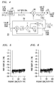
- FIG. 3 is a block diagram of one embodiment of a device for digitally shaping the quantization noise of an N-bit digital signal in accordance with the invention.
- an N-bit digital signal N being a positive integer
- register 230 digital signals designated by upper case letters, such as X+E o in FIG. 3, represent the Z-transformed version of a corresponding time or sampled data domain signal, typically designated by corresponding lower case letters, such as x(n)+e o (n), where n is an arbitrary signal index.
- Register 230 masks N-M selected bits of the N-bit digital signal to provide an M-bit digital signal, M being a positive integer less than N.
- masking selected bits of an N-bit digital signal refers to a process in which selected bits are removed from or "masked out" of the N-bit digital signal. This may be accomplished, for example, by a logical AND operation between the selected bits, i.e., the digital binary signals in the selected bit locations of the N-bit digital signal, and zero.
- masking register 230 may operate as a truncator that truncates the N-M selected bits of the N-bit digital signal.
- the N-M selected bits are the N-M least significant bits of the N-bit digital signal.
- register 230 truncates the N-M least significant bits of the N-bit digital signal
- a truncation error designated E 1 in FIG. 3 is introduced into the N-bit digital signal produced by register 230.
- E 1 a truncation error
- X+E o represents the N-bit digital signal, including its error E o , provided to register 230
- X+ E o - E 1 represents the M-bit digital signal produced by register 230.
- the N-M masked bits are then provided to a digital noise-shaping coder 240.
- the truncation error E 1 corresponding to the N-M least significant bits of the N-bit digital signal, is now provided to digital noise-shaping coder 240.
- the digital noise-shaping coder may comprise, without limitation, a sigma-delta modulator, such as one of the type illustrated in FIG. 4.
- the digital noise-shaping coder may comprise a coder of any number of bits, such as a one-bit coder or a multi-bit coder.
- the digital noise-shaping coder may have any order filter in its feedback path, its feed forward path, or both, and, in addition, it may have multiple feed forward loops, multiple feedback loops, or both.
- the digital noise-shaping coder may be multi-staged or cascaded. Thus, in general, depending on the particular application, any digital noise-shaping coder will suffice in which at least a portion of the in-band quantization noise of the coder is reduced at the expense of a portion of the out-of-band quantization noise.
- digitally shaping the quantization noise refers to a process whereby the power spectral density associated with the quantization error is shaped by digital filtering so that at least a portion of the amount of noise energy present over a predetermined range of relevant frequencies is reduced.
- the N-M bit digital signal may be superpositioned with a digitally filtered error signal, filtered by a digital noise-shaping filter H(z)-1, and then "requantized” by quantizer 310.
- This "requantized” digital signal is compared with the superpositioned digital signal before “requantization” to produce the "requantization” error signal, designated E 2 in FIG. 3.
- This "requantization” error signal, E 2 is the error signal mentioned above, filtered by the digital noise-shaping filter, H(z)-1, and summed or superpositioned with the N-M bit digital signal provided by register 230.
- Digital noise-shaping filters are described in more detail in the aforementioned "Oversampling Methods for A/D and D/A Conversion” and “Oversampled, Linear Predictive and Noise-Shaping Coders of Order N>1.”
- the result of this digital signal processing is to produce a B-bit digital signal, B being a positive integer less than N-M, that may be summed or superpositioned with the M-bit digital signal at node or accumulator 260 to provide an M+B bit digital signal, M + B being a positive integer less than N. It may be desirable for the digital signal produced by the digital noise-shaping coder to be represented as either a positive or negative signal.
- one of the bits at the B bit digital signal functions as a sign bit, and the digital signal produced at accumulator 260 may therefore comprise M+B-1 bits rather than M+B bits.
- the result of embodiment 200 is to requantize digital signal X + E o into another digital signal having fewer bits, for further signal processing. Furthermore, the quantization, or requantization, noise introduced by this process has been digitally shaped so that it is negligible in comparison with the noise, E o , of the initial signal E o . Likewise, as illustrated in FIG. 3, this requantized digital signal may be provided to a conventional digital-to-analog converter 270 to produce an analog output signal. Nonetheless, due to the digital shaping of the quantization noise accomplished, the hardware complexity of DAC 270 is reduced, at least in part, because the digital signal provided to the DAC has fewer bits than the initial digital signal.
- embodiment 200 of a device for shaping the quantization noise of an N-bit digital signal in accordance with the invention may also be employed in a device for converting an N-bit digital signal to an analog signal to achieve some advantages over conventional digital-to-analog conversion approaches.
- the N-M least significant bits of the N-bit digital signal are masked by register 230
- the invention is not so limited in scope.
- a field of bits in the N-bit digital signal, other than the least significant bits may be masked. In the context of the invention, this is referred to as "digital signal bit field ranging.”
- non-contiguous bits may be masked, depending on the particular application.
- quantizer 310 illustrated in FIG. 3 may comprise either a 1-bit quantizer or a multibit quantizer.
- One advantage of employing a 1-bit quantizer is the inherent linearity associated with only employing two digital signal output levels, particularly for small input signals where a substantial amount of the signal energy passes through the digital noise-shaping coder. Nonetheless, other advantages may result from the use of a multibit quantizer as well. For example, if a 2 or 3-bit quantizer is employed, overload due to the truncation error provided to the digital noise-shaping coder may be avoided. Furthermore, as previously suggested, the architecture illustrated in FIG. 3 offers advantages in comparison with the approach in FIG. 1 in that fewer conversion levels for the DAC are required, thereby reducing the linearity problem presented.
- An advantage offered by the architecture illustrated in FIG. 3 in comparison with the architecture illustrated in FIG. 2 includes exact cancellation of the truncation error.
- the truncation error is introduced when the N-bit digital signal is converted to an M-bit digital signal, the M bits being the most significant bits of the N-bit digital signal in this particular embodiment. Exact cancellation or correction, however, occurs because the summation or superposition of the two digital signals at accumulator 260 in FIG. 3 is performed in the digital domain, as opposed to the analog domain as illustrated in FIG. 2.
- the problem of analog mismatches between two different DACs, such as DAC 120 and DAC 160 in FIG. 2 is avoided.
- a sigma-delta modulator such as modulator 250 in FIG. 4, in place of digital noise-shaping coder 240. Nonetheless, as previously discussed, the invention is not restricted in scope to the particular embodiments of a digital noise-shaping coder or sigma-delta modulator illustrated. In contrast with the previously-described digital noise-shaping coder and as explained in more detail in the aforementioned "Oversampled, Linear Predictive and Noise-Shaping Coders of Order N>1," in FIG. 4 the N-M bits of the N-bit digital signal corresponding to truncation error E 1 are offset with the digital output signal of the sigma-delta modulator.
- the digital output signal of sigma-delta modulator 250 is the requantized, digitally-filtered, N-M bits offset by the digital signal output of the sigma-delta modulator.
- the quantizer such as quantizer 320 in FIG. 4, may be either 1-bit or multibit.
- the sigma-delta modulator may be designed to an arbitrarily high order of noise shaping and still remain stable. This provides an advantage in that a reduction of the oversampling ratio, for an oversampled sigma-delta modulator, may be employed, thereby improving the usable speed and bandwidth of digital-to-analog converter 270 without a degradation in the signal-to-noise ratio in the baseband.
- a DAC of reduced hardware complexity may be employed. It will, of course, be appreciated that if an oversampled sigma-delta modulator is employed, the digital-to-analog conversion system illustrated in FIG. 4 comprises the system after interpolation from a lower sampling rate has taken place. Thus, the digital signal provided to register 230 is already oversampled.
- FIGs. 3 and 4 illustrate yet other embodiments of a device for shaping the quantization noise of an N-bit digital signal in accordance with the invention.
- high-level dither such as described in U.S. Patent No. 5,144,308, entitled “Idle Channel Tone and Periodic Noise Suppression for Sigma-Delta Modulators using High Level Dither," by Norsworthy, issued September 1, 1992, assigned to the assignee of the present invention, is illustrated in phantom.
- D represents the Z-transformed version of a time or sampled data domain dither signal, d(n). As illustrated in FIGs.
- dithering may be accomplished by superpositioning or adding a dither signal, typically white noise, such as may be produced by a dither signal generator, to the digital signal of the sigma-delta modulator, illustrated in FIG. 4, or the digital noise-shaping coder, illustrated in FIG. 3, before the quantizer quantizes the digital signal.
- a sigma-delta modulator that also performs dithering, such as illustrated in FIG. 4, is referred to as a dithered sigma-delta modulator.
- a device for digitally shaping the quantization noise of an N-bit digital signal may operate in accordance with the following method.
- An N-bit digital signal is provided to masking register 230. Selected bits of the N-bit digital signal are masked to produce an M-bit digital signal, M being a positive integer less than N.
- the N-bit digital signal is truncated.
- the N-M masked or truncated bits of the N-bit digital signal are digitally coded, in the embodiment illustrated in FIG. 3 the N-M least significant bits, to provide a B-bit digital signal, B being a positive integer less than N-M.
- many different digital noise-shaping coders other than the embodiment illustrated in FIG.
- the M-bit digital signal produced from the N-bit digital signal and the B-bit digital signal produced from the N-M bit digital signal are then accumulated by accumulator or summing note 260.
- a conventional digital-to-analog converter such as DAC 270, may convert the accumulated digital signal to an analog signal.
- digitally coding the masked N-M bits of the N-bit digital signal may comprise sigma-delta modulating the N-M bits.
- dithering may also be included.
- the step of sigma-delta modulating the remaining bits of the N-bit digital signal other than the M-bits includes quantizing a digitally-filtered signal, such as illustrated in FIG. 3, the step of sigma-delta modulating the remaining or masked N-M bits comprises superpositioning a dither signal, as previously discussed, with the digitally-filtered signal and quantizing, or "requantizing," the superpositioned digital signal.
- FIGs. 5 and 6 are, respectively, plots of simulation results illustrating the performance of a multibit sigma-delta modulator, such as illustrated in FIG. 1, with a device for digitally shaping the quantization noise of an N-bit digital signal in accordance with the invention having the architecture of the embodiment illustrated in FIG. 4.
- a 16-bit sine wave was provided to a second-order multibit digital sigma-delta modulator.
- the quantizer of the modulator was 10 bits.
- the output signal of the quantizer was then provided an "ideal" 10-bit DAC.
- the oversampling ratio employed was 16. This produced a baseband noise floor of -105.1 dB.
- the spectrum produced is illustrated in FIG.
- the digital noise shaping employed to produce FIG. 6 introduced some slight additional error into the resulting signal, however, this error is negligible in comparison with the initial baseband noise floor.
- a reduction in the complexity of the hardware in this case a reduction from a 16-bit digital signal path to an 8-bit digital signal path for the sigma-delta modulator, was achieved without a substantial degradation in the quality of the digital signal obtained.
Landscapes
- Engineering & Computer Science (AREA)
- Theoretical Computer Science (AREA)
- Computer Networks & Wireless Communication (AREA)
- Signal Processing (AREA)
- Physics & Mathematics (AREA)
- General Engineering & Computer Science (AREA)
- General Physics & Mathematics (AREA)
- Compression, Expansion, Code Conversion, And Decoders (AREA)
- Transmission Systems Not Characterized By The Medium Used For Transmission (AREA)
- Analogue/Digital Conversion (AREA)
Claims (9)
- Dispositif (par exemple 215, 220) pour façonner numériquement le bruit de quantification d'un signal numérique à N-bits, N étant un entier positif, caractérisé en ce que ledit dispositif (par exemple 215, 220) comporte :un registre (par exemple 230) destiné à enlever par masquage des bits choisis du signal numérique à N-bits pour produire un signal numérique à M-bits, M étant un entier positif inférieur à N ;un codeur (par exemple 240, 250) de configuration de bruit numérique, couplé audit registre (par exemple 230), pour façonner le bruit de quantification des bits enlevés par masquage afin de produire un signal numérique à B-bits, B étant un entier positif inférieur à N-M ; etun accumulateur (par exemple 260), couplé audit registre (par exemple 230) et audit codeur (par exemple 240, 250), pour accumuler les signaux numériques reçus dudit registre (par exemple 230) et dudit codeur (par exemple 240, 250).
- Dispositif (par exemple 215, 220) selon la revendication 1, dans lequel ledit registre (par exemple 230) comporte un élément à troncature (par exemple 230) ; et
dans lequel les bits enlevés par masquage comprennent les N-M bits de poids faible du signal numérique à N-bits. - Dispositif (par exemple 215, 220) selon la revendication 1, dans lequel ledit codeur (par exemple 240) comprend un codeur (par exemple 240) de façonnage de bruit numérique à bits multiples.
- Dispositif (par exemple 215, 220) selon la revendication 1, dans lequel ledit codeur (par exemple 240, 250) comprend un modulateur sigma-delta (par exemple 250) à bits multiples.
- Dispositif (par exemple 215, 220) selon la revendication 1, et comportant en outre :
un convertisseur numérique-analogique (par exemple 270), couplé audit accumulateur (par exemple 260), pour convertir le signal numérique reçu dudit accumulateur (par exemple 260) en un signal analogique. - Procédé pour façonner numériquement le bruit de quantification d'un signal numérique à N-bits, N étant un entier positif, caractérisé en ce que ledit procédé comprend les étapes dans lesquelles :on masque des bits choisis du signal numérique à N-bits pour produire un signal numérique à M-bits, M étant un entier positif inférieur à N ;on code numériquement les bits masqués du signal à N-bits pour produire un signal numérique à B-bits, B étant un entier positif inférieur à N-M ; eton accumule le signal numérique à M-bits et le signal numérique à B-bits.
- Procédé selon la revendication 6, dans lequel l'étape de masquage comprend la troncature du signal numérique à N-bits pour produire le signal numérique à M-bits ; et
dans lequel le signal numérique à N-bits comprend les M-bits de poids fort du signal numérique à N-bits, M étant un entier positif supérieur à un. - Procédé selon la revendication 7, dans lequel l'étape de collage numérique des bits masqués comprend une modulation sigma-delta des bits masqués.
- Procédé selon la revendication 6, et comprenant en outre l'étape de conversion du signal numérique accumulé en un signal analogique.
Applications Claiming Priority (2)
| Application Number | Priority Date | Filing Date | Title |
|---|---|---|---|
| US171485 | 1993-12-21 | ||
| US08/171,485 US5424739A (en) | 1993-12-21 | 1993-12-21 | Device and method for digitally shaping the quantization noise of an N-bit digital signal, such as for digital-to-analog conversion |
Publications (3)
| Publication Number | Publication Date |
|---|---|
| EP0660532A2 EP0660532A2 (fr) | 1995-06-28 |
| EP0660532A3 EP0660532A3 (fr) | 1996-06-05 |
| EP0660532B1 true EP0660532B1 (fr) | 2001-10-31 |
Family
ID=22623903
Family Applications (1)
| Application Number | Title | Priority Date | Filing Date |
|---|---|---|---|
| EP94309008A Expired - Lifetime EP0660532B1 (fr) | 1993-12-21 | 1994-12-05 | Procédé et dispositif pour la mise en forme numérique du bruit de quantification d'un signal à n-bit par example pour la conversion numérique analogique |
Country Status (6)
| Country | Link |
|---|---|
| US (1) | US5424739A (fr) |
| EP (1) | EP0660532B1 (fr) |
| JP (1) | JPH07212236A (fr) |
| KR (1) | KR0174028B1 (fr) |
| DE (1) | DE69428869T2 (fr) |
| TW (1) | TW252240B (fr) |
Families Citing this family (29)
| Publication number | Priority date | Publication date | Assignee | Title |
|---|---|---|---|---|
| US5602874A (en) * | 1994-12-29 | 1997-02-11 | Motorola, Inc. | Method and apparatus for reducing quantization noise |
| US5745061A (en) * | 1995-07-28 | 1998-04-28 | Lucent Technologies Inc. | Method of improving the stability of a sigma-delta modulator employing dither |
| DE69623749D1 (de) * | 1996-02-23 | 2002-10-24 | St Microelectronics Srl | Eingabe eines Rausch-weissenden Signals in einem bei der Wandlung digitaler Audiosignale angewandten Sigma-Delta-Modulator |
| CA2286978A1 (fr) * | 1997-04-18 | 1998-10-29 | Jesper Steensgaard-Madsen | Denumeriseur surechantillonne base sur la separation non lineaire et la recombinaison lineaire |
| US5835038A (en) * | 1997-05-08 | 1998-11-10 | Burr-Brown Corporation | DC dither circuitry and method for delta-sigma modulator |
| FR2765419B1 (fr) * | 1997-06-27 | 1999-09-17 | Thomson Csf | Dispositif de generation de signaux analogiques a partir de convertisseurs analogique-numerique, notamment pour la synthese numerique directe |
| US6137809A (en) * | 1997-08-22 | 2000-10-24 | Paradyne Corporation | Quantization noise compensator apparatus and method |
| US6326911B1 (en) * | 1997-11-19 | 2001-12-04 | Texas Instruments Incorporated | Method and apparatus for dithering idle channel tones in delta-sigma analog-to-digital converters |
| US6366622B1 (en) | 1998-12-18 | 2002-04-02 | Silicon Wave, Inc. | Apparatus and method for wireless communications |
| US6355537B1 (en) | 1999-02-23 | 2002-03-12 | Silicon Wave, Inc. | Method of providing radio frequency isolation of device mesas using guard ring regions within an integrated circuit device |
| JP2000269821A (ja) * | 1999-03-18 | 2000-09-29 | Oki Micro Design Co Ltd | 予測符号化信号復号化装置及び雑音除去方法 |
| US6627954B1 (en) | 1999-03-19 | 2003-09-30 | Silicon Wave, Inc. | Integrated circuit capacitor in a silicon-on-insulator integrated circuit |
| AUPQ122699A0 (en) * | 1999-06-25 | 1999-07-22 | Lake Dsp Pty Limited | Sigma delta modulator with buried data |
| DE19935840A1 (de) * | 1999-07-29 | 2001-03-08 | Siemens Ag | Schaltungsanordnung zur Abtastratenumsetzung zeitdiskreter Signale |
| JP2001077692A (ja) | 1999-09-02 | 2001-03-23 | Nec Ic Microcomput Syst Ltd | D/a変換回路 |
| US6429502B1 (en) | 2000-08-22 | 2002-08-06 | Silicon Wave, Inc. | Multi-chambered trench isolated guard ring region for providing RF isolation |
| WO2002023731A2 (fr) * | 2000-09-11 | 2002-03-21 | Broadcom Corporation | Procedes et systemes pour application de signaux de vibration |
| WO2003001677A2 (fr) * | 2001-06-21 | 2003-01-03 | Nokia Corporation | Convertisseur numerique/analogique et procede de conversion numerique/analogique |
| US7145936B2 (en) * | 2002-12-23 | 2006-12-05 | International Business Machines Corporation | Bandpass delta sigma truncator and method of truncating a multi-bit digital signal |
| US6822594B1 (en) * | 2003-10-09 | 2004-11-23 | Cirrus Logic, Inc. | Overload protection and stability for high order 1-bit delta-sigma modulators |
| EP1712004A2 (fr) | 2004-01-28 | 2006-10-18 | Koninklijke Philips Electronics N.V. | Systeme de convertisseur numerique-analogique et procede de conversion d'un signal numerique multibits en un signal analogique |
| US7321634B2 (en) * | 2004-12-17 | 2008-01-22 | Verigy (Singapore) Pte. Ltd. | Method and apparatus for variable sigma-delta modulation |
| US7425910B1 (en) | 2006-02-27 | 2008-09-16 | Marvell International Ltd. | Transmitter digital-to-analog converter with noise shaping |
| KR101593729B1 (ko) * | 2009-03-31 | 2016-02-15 | 에이저 시스템즈 엘엘시 | 입력 신호로부터 rf 신호를 합성하기 위한 방법, 델타-시그마 변조기 및 집적 회로 |
| DE102010043842A1 (de) * | 2010-11-12 | 2012-05-16 | Endress + Hauser Wetzer Gmbh + Co Kg | Delta-Sigma-D/A-Wandler |
| DE102014104142B4 (de) * | 2014-03-25 | 2015-10-22 | Intel IP Corporation | Quantisierungsschaltung und Verfahren zum Quantisieren einer Eingangsgröße |
| DE102014113951B4 (de) | 2014-09-26 | 2017-07-13 | Intel IP Corporation | Eine Schaltung, eine integrierte Schaltung, ein Sender, ein Empfänger, ein Sendeempfänger, ein Verfahren zum Erzeugen eines verarbeiteten Oszillatorsignals, eine Vorrichtung zum Erzeugen eines verarbeiteten Oszillatorsignals und softwarebezogene Implementierungen |
| EP3309781B1 (fr) * | 2015-06-10 | 2023-10-04 | Sony Group Corporation | Dispositif de traitement de signal, procédé de traitement de signal, et programme |
| US11581901B2 (en) * | 2020-09-21 | 2023-02-14 | Apple Inc. | Digital pre-distortion compensation of digital-to-analog converter non-linearity |
Family Cites Families (3)
| Publication number | Priority date | Publication date | Assignee | Title |
|---|---|---|---|---|
| DE3021012C2 (de) * | 1980-06-03 | 1985-08-22 | ANT Nachrichtentechnik GmbH, 7150 Backnang | Verallgemeinertes interpolativers Verfahren zur Digital-Analog-Umsetzung von PCM Signalen |
| US4593271A (en) * | 1985-01-16 | 1986-06-03 | At&T Bell Laboratories | Higher order interpolation for digital-to-analog conversion |
| US5144308A (en) * | 1991-05-21 | 1992-09-01 | At&T Bell Laboratories | Idle channel tone and periodic noise suppression for sigma-delta modulators using high-level dither |
-
1993
- 1993-12-21 US US08/171,485 patent/US5424739A/en not_active Expired - Lifetime
-
1994
- 1994-04-23 TW TW083103627A patent/TW252240B/zh not_active IP Right Cessation
- 1994-12-05 EP EP94309008A patent/EP0660532B1/fr not_active Expired - Lifetime
- 1994-12-05 DE DE69428869T patent/DE69428869T2/de not_active Expired - Lifetime
- 1994-12-16 KR KR1019940034606A patent/KR0174028B1/ko not_active IP Right Cessation
- 1994-12-19 JP JP6313904A patent/JPH07212236A/ja active Pending
Also Published As
| Publication number | Publication date |
|---|---|
| JPH07212236A (ja) | 1995-08-11 |
| DE69428869T2 (de) | 2002-07-11 |
| KR0174028B1 (ko) | 1999-04-01 |
| DE69428869D1 (de) | 2001-12-06 |
| EP0660532A2 (fr) | 1995-06-28 |
| KR950022176A (ko) | 1995-07-28 |
| US5424739A (en) | 1995-06-13 |
| TW252240B (fr) | 1995-07-21 |
| EP0660532A3 (fr) | 1996-06-05 |
Similar Documents
| Publication | Publication Date | Title |
|---|---|---|
| EP0660532B1 (fr) | Procédé et dispositif pour la mise en forme numérique du bruit de quantification d'un signal à n-bit par example pour la conversion numérique analogique | |
| US6304608B1 (en) | Multibit sigma-delta converters employing dynamic element matching with reduced baseband tones | |
| US5329282A (en) | Multi-bit sigma-delta analog-to-digital converter with reduced sensitivity to DAC nonlinearities | |
| US7002497B2 (en) | Methods and systems for digital dither | |
| US5977899A (en) | Digital-to-analog converter using noise-shaped segmentation | |
| EP1402644B1 (fr) | Procede et appareil de suppression de signaux sonores induits par des algorithmes de concordance d'elements dynamiques cycliques (dem) | |
| US5682161A (en) | High-order delta sigma modulator | |
| US6518899B2 (en) | Method and apparatus for spectral shaping of non-linearity in data converters | |
| US6697003B1 (en) | System and method for dynamic element matching | |
| EP1488525B1 (fr) | Systeme et procede permettant d'obtenir une modulation sigma-delta adaptive | |
| US6326911B1 (en) | Method and apparatus for dithering idle channel tones in delta-sigma analog-to-digital converters | |
| US7453382B2 (en) | Method and apparatus for A/D conversion | |
| US6515606B2 (en) | Analog to digital converter | |
| US5530442A (en) | Circuit and method for testing a dithered analog-to-digital converter | |
| KR100196518B1 (ko) | 오디오용 델타-시그마 변조기 | |
| US5446460A (en) | Fourth-order cascaded sigma-delta modulator | |
| US5629701A (en) | Cascaded Nth order (N>2) feedforward sigma-delta modulators | |
| JP3785361B2 (ja) | Δςモジュレータ、a/dコンバータおよびd/aコンバータ | |
| US6028544A (en) | Digital-to-analog converter with noiseshaping modulator, commutator and plurality of unit converters, and method | |
| Candy et al. | Oversampling methods for data conversion | |
| US7009539B2 (en) | Modulator providing only quantization error component to delta sigma modulator | |
| Norsworthy et al. | A minimal multibit digital noise shaping architecture | |
| Fang et al. | A multi-bit sigma-delta modulator with interstate feedback | |
| JP3040546B2 (ja) | ノイズシェーピングa−d変換器 | |
| JPH11308110A (ja) | デルタシグマ型アナログデジタル変換器 |
Legal Events
| Date | Code | Title | Description |
|---|---|---|---|
| PUAI | Public reference made under article 153(3) epc to a published international application that has entered the european phase |
Free format text: ORIGINAL CODE: 0009012 |
|
| AK | Designated contracting states |
Kind code of ref document: A2 Designated state(s): DE ES FR GB IT NL |
|
| PUAL | Search report despatched |
Free format text: ORIGINAL CODE: 0009013 |
|
| RHK1 | Main classification (correction) |
Ipc: H03M 7/00 |
|
| AK | Designated contracting states |
Kind code of ref document: A3 Designated state(s): DE ES FR GB IT NL |
|
| 17P | Request for examination filed |
Effective date: 19961120 |
|
| GRAG | Despatch of communication of intention to grant |
Free format text: ORIGINAL CODE: EPIDOS AGRA |
|
| 17Q | First examination report despatched |
Effective date: 20001016 |
|
| GRAG | Despatch of communication of intention to grant |
Free format text: ORIGINAL CODE: EPIDOS AGRA |
|
| GRAH | Despatch of communication of intention to grant a patent |
Free format text: ORIGINAL CODE: EPIDOS IGRA |
|
| GRAH | Despatch of communication of intention to grant a patent |
Free format text: ORIGINAL CODE: EPIDOS IGRA |
|
| GRAA | (expected) grant |
Free format text: ORIGINAL CODE: 0009210 |
|
| AK | Designated contracting states |
Kind code of ref document: B1 Designated state(s): DE ES FR GB IT NL |
|
| PG25 | Lapsed in a contracting state [announced via postgrant information from national office to epo] |
Ref country code: NL Free format text: LAPSE BECAUSE OF FAILURE TO SUBMIT A TRANSLATION OF THE DESCRIPTION OR TO PAY THE FEE WITHIN THE PRESCRIBED TIME-LIMIT Effective date: 20011031 Ref country code: IT Free format text: LAPSE BECAUSE OF FAILURE TO SUBMIT A TRANSLATION OF THE DESCRIPTION OR TO PAY THE FEE WITHIN THE PRESCRIBED TIME-LIMIT;WARNING: LAPSES OF ITALIAN PATENTS WITH EFFECTIVE DATE BEFORE 2007 MAY HAVE OCCURRED AT ANY TIME BEFORE 2007. THE CORRECT EFFECTIVE DATE MAY BE DIFFERENT FROM THE ONE RECORDED. Effective date: 20011031 Ref country code: FR Free format text: LAPSE BECAUSE OF FAILURE TO SUBMIT A TRANSLATION OF THE DESCRIPTION OR TO PAY THE FEE WITHIN THE PRESCRIBED TIME-LIMIT Effective date: 20011031 |
|
| PGFP | Annual fee paid to national office [announced via postgrant information from national office to epo] |
Ref country code: NL Payment date: 20011113 Year of fee payment: 8 |
|
| PGFP | Annual fee paid to national office [announced via postgrant information from national office to epo] |
Ref country code: ES Payment date: 20011205 Year of fee payment: 8 |
|
| REF | Corresponds to: |
Ref document number: 69428869 Country of ref document: DE Date of ref document: 20011206 |
|
| REG | Reference to a national code |
Ref country code: GB Ref legal event code: IF02 |
|
| NLV1 | Nl: lapsed or annulled due to failure to fulfill the requirements of art. 29p and 29m of the patents act | ||
| PG25 | Lapsed in a contracting state [announced via postgrant information from national office to epo] |
Ref country code: ES Free format text: LAPSE BECAUSE OF FAILURE TO SUBMIT A TRANSLATION OF THE DESCRIPTION OR TO PAY THE FEE WITHIN THE PRESCRIBED TIME-LIMIT Effective date: 20020430 |
|
| PLBE | No opposition filed within time limit |
Free format text: ORIGINAL CODE: 0009261 |
|
| STAA | Information on the status of an ep patent application or granted ep patent |
Free format text: STATUS: NO OPPOSITION FILED WITHIN TIME LIMIT |
|
| 26N | No opposition filed | ||
| PGFP | Annual fee paid to national office [announced via postgrant information from national office to epo] |
Ref country code: FR Payment date: 20021227 Year of fee payment: 9 |
|
| PGFP | Annual fee paid to national office [announced via postgrant information from national office to epo] |
Ref country code: DE Payment date: 20131127 Year of fee payment: 20 Ref country code: GB Payment date: 20131204 Year of fee payment: 20 |
|
| REG | Reference to a national code |
Ref country code: DE Ref legal event code: R071 Ref document number: 69428869 Country of ref document: DE |
|
| REG | Reference to a national code |
Ref country code: GB Ref legal event code: PE20 Expiry date: 20141204 |
|
| PG25 | Lapsed in a contracting state [announced via postgrant information from national office to epo] |
Ref country code: GB Free format text: LAPSE BECAUSE OF EXPIRATION OF PROTECTION Effective date: 20141204 |