EP0659011A2 - Schwankungs- und Bogenkorrektur durch Intensitätsproportionierung von zwei Bildelementpunkten - Google Patents
Schwankungs- und Bogenkorrektur durch Intensitätsproportionierung von zwei Bildelementpunkten Download PDFInfo
- Publication number
- EP0659011A2 EP0659011A2 EP94307160A EP94307160A EP0659011A2 EP 0659011 A2 EP0659011 A2 EP 0659011A2 EP 94307160 A EP94307160 A EP 94307160A EP 94307160 A EP94307160 A EP 94307160A EP 0659011 A2 EP0659011 A2 EP 0659011A2
- Authority
- EP
- European Patent Office
- Prior art keywords
- diodes
- scan
- selecting
- light beams
- spot
- Prior art date
- Legal status (The legal status is an assumption and is not a legal conclusion. Google has not performed a legal analysis and makes no representation as to the accuracy of the status listed.)
- Granted
Links
Images


Classifications
-
- H—ELECTRICITY
- H04—ELECTRIC COMMUNICATION TECHNIQUE
- H04N—PICTORIAL COMMUNICATION, e.g. TELEVISION
- H04N1/00—Scanning, transmission or reproduction of documents or the like, e.g. facsimile transmission; Details thereof
- H04N1/04—Scanning arrangements, i.e. arrangements for the displacement of active reading or reproducing elements relative to the original or reproducing medium, or vice versa
- H04N1/047—Detection, control or error compensation of scanning velocity or position
- H04N1/0473—Detection, control or error compensation of scanning velocity or position in subscanning direction, e.g. picture start or line-to-line synchronisation
-
- G—PHYSICS
- G06—COMPUTING; CALCULATING OR COUNTING
- G06K—GRAPHICAL DATA READING; PRESENTATION OF DATA; RECORD CARRIERS; HANDLING RECORD CARRIERS
- G06K15/00—Arrangements for producing a permanent visual presentation of the output data, e.g. computer output printers
- G06K15/02—Arrangements for producing a permanent visual presentation of the output data, e.g. computer output printers using printers
- G06K15/12—Arrangements for producing a permanent visual presentation of the output data, e.g. computer output printers using printers by photographic printing, e.g. by laser printers
- G06K15/1204—Arrangements for producing a permanent visual presentation of the output data, e.g. computer output printers using printers by photographic printing, e.g. by laser printers involving the fast moving of an optical beam in the main scanning direction
- G06K15/1219—Detection, control or error compensation of scanning velocity or position, e.g. synchronisation
-
- H—ELECTRICITY
- H04—ELECTRIC COMMUNICATION TECHNIQUE
- H04N—PICTORIAL COMMUNICATION, e.g. TELEVISION
- H04N1/00—Scanning, transmission or reproduction of documents or the like, e.g. facsimile transmission; Details thereof
- H04N1/04—Scanning arrangements, i.e. arrangements for the displacement of active reading or reproducing elements relative to the original or reproducing medium, or vice versa
- H04N1/113—Scanning arrangements, i.e. arrangements for the displacement of active reading or reproducing elements relative to the original or reproducing medium, or vice versa using oscillating or rotating mirrors
- H04N1/1135—Scanning arrangements, i.e. arrangements for the displacement of active reading or reproducing elements relative to the original or reproducing medium, or vice versa using oscillating or rotating mirrors for the main-scan only
-
- H—ELECTRICITY
- H04—ELECTRIC COMMUNICATION TECHNIQUE
- H04N—PICTORIAL COMMUNICATION, e.g. TELEVISION
- H04N1/00—Scanning, transmission or reproduction of documents or the like, e.g. facsimile transmission; Details thereof
- H04N1/04—Scanning arrangements, i.e. arrangements for the displacement of active reading or reproducing elements relative to the original or reproducing medium, or vice versa
- H04N1/12—Scanning arrangements, i.e. arrangements for the displacement of active reading or reproducing elements relative to the original or reproducing medium, or vice versa using the sheet-feed movement or the medium-advance or the drum-rotation movement as the slow scanning component, e.g. arrangements for the main-scanning
-
- H—ELECTRICITY
- H04—ELECTRIC COMMUNICATION TECHNIQUE
- H04N—PICTORIAL COMMUNICATION, e.g. TELEVISION
- H04N1/00—Scanning, transmission or reproduction of documents or the like, e.g. facsimile transmission; Details thereof
- H04N1/04—Scanning arrangements, i.e. arrangements for the displacement of active reading or reproducing elements relative to the original or reproducing medium, or vice versa
- H04N1/19—Scanning arrangements, i.e. arrangements for the displacement of active reading or reproducing elements relative to the original or reproducing medium, or vice versa using multi-element arrays
- H04N1/191—Scanning arrangements, i.e. arrangements for the displacement of active reading or reproducing elements relative to the original or reproducing medium, or vice versa using multi-element arrays the array comprising a one-dimensional array, or a combination of one-dimensional arrays, or a substantially one-dimensional array, e.g. an array of staggered elements
- H04N1/1911—Simultaneously or substantially simultaneously scanning picture elements on more than one main scanning line, e.g. scanning in swaths
-
- H—ELECTRICITY
- H04—ELECTRIC COMMUNICATION TECHNIQUE
- H04N—PICTORIAL COMMUNICATION, e.g. TELEVISION
- H04N2201/00—Indexing scheme relating to scanning, transmission or reproduction of documents or the like, and to details thereof
- H04N2201/024—Indexing scheme relating to scanning, transmission or reproduction of documents or the like, and to details thereof deleted
- H04N2201/02406—Arrangements for positioning elements within a head
- H04N2201/02439—Positioning method
- H04N2201/02441—Positioning method using screws
-
- H—ELECTRICITY
- H04—ELECTRIC COMMUNICATION TECHNIQUE
- H04N—PICTORIAL COMMUNICATION, e.g. TELEVISION
- H04N2201/00—Indexing scheme relating to scanning, transmission or reproduction of documents or the like, and to details thereof
- H04N2201/04—Scanning arrangements
- H04N2201/047—Detection, control or error compensation of scanning velocity or position
- H04N2201/04701—Detection of scanning velocity or position
- H04N2201/0471—Detection of scanning velocity or position using dedicated detectors
-
- H—ELECTRICITY
- H04—ELECTRIC COMMUNICATION TECHNIQUE
- H04N—PICTORIAL COMMUNICATION, e.g. TELEVISION
- H04N2201/00—Indexing scheme relating to scanning, transmission or reproduction of documents or the like, and to details thereof
- H04N2201/04—Scanning arrangements
- H04N2201/047—Detection, control or error compensation of scanning velocity or position
- H04N2201/04701—Detection of scanning velocity or position
- H04N2201/04734—Detecting at frequent intervals, e.g. once per line for sub-scan control
-
- H—ELECTRICITY
- H04—ELECTRIC COMMUNICATION TECHNIQUE
- H04N—PICTORIAL COMMUNICATION, e.g. TELEVISION
- H04N2201/00—Indexing scheme relating to scanning, transmission or reproduction of documents or the like, and to details thereof
- H04N2201/04—Scanning arrangements
- H04N2201/047—Detection, control or error compensation of scanning velocity or position
- H04N2201/04701—Detection of scanning velocity or position
- H04N2201/04744—Detection of scanning velocity or position by detecting the scanned beam or a reference beam
-
- H—ELECTRICITY
- H04—ELECTRIC COMMUNICATION TECHNIQUE
- H04N—PICTORIAL COMMUNICATION, e.g. TELEVISION
- H04N2201/00—Indexing scheme relating to scanning, transmission or reproduction of documents or the like, and to details thereof
- H04N2201/04—Scanning arrangements
- H04N2201/047—Detection, control or error compensation of scanning velocity or position
- H04N2201/04701—Detection of scanning velocity or position
- H04N2201/04749—Detecting position relative to a gradient, e.g. using triangular-shaped masks, marks or gratings
-
- H—ELECTRICITY
- H04—ELECTRIC COMMUNICATION TECHNIQUE
- H04N—PICTORIAL COMMUNICATION, e.g. TELEVISION
- H04N2201/00—Indexing scheme relating to scanning, transmission or reproduction of documents or the like, and to details thereof
- H04N2201/04—Scanning arrangements
- H04N2201/047—Detection, control or error compensation of scanning velocity or position
- H04N2201/04753—Control or error compensation of scanning position or velocity
- H04N2201/04758—Control or error compensation of scanning position or velocity by controlling the position of the scanned image area
-
- H—ELECTRICITY
- H04—ELECTRIC COMMUNICATION TECHNIQUE
- H04N—PICTORIAL COMMUNICATION, e.g. TELEVISION
- H04N2201/00—Indexing scheme relating to scanning, transmission or reproduction of documents or the like, and to details thereof
- H04N2201/04—Scanning arrangements
- H04N2201/047—Detection, control or error compensation of scanning velocity or position
- H04N2201/04753—Control or error compensation of scanning position or velocity
- H04N2201/04794—Varying the control or compensation during the scan, e.g. using continuous feedback or from line to line
- H04N2201/04796—Varying the sub-scan control during the main-scan, e.g. for correcting skew, tilt or bow of a scanning beam
Definitions
- This invention relates to a raster scanning system, and more particularly, to a raster scanning system which utilizes a dual light source for wobble correction caused by different factors such as an imperfect facet of a scanning polygon.
- a raster scanner typically includes a number of optical elements to accommodate a specific design. Unavoidable imprecision in the shape and/or mounting of these optical elements will inevitably introduce certain anomalies in the quality of the scan line on the photoreceptor such as wobble or bow.
- Wobble is defined as the displacement of a scan line in the cross-scan or sagittal plane from its intended position.
- a wobble error in an optical scanning system is caused by different factors such as the rotating facet not being exactly parallel to the vertical axis. In this case, the beam reflected from the facet is thereby angled up or down for a small amount resulting in scan line displacement errors in the sagittal plane.
- Wobble errors can be caused by several factors.
- the motor driving the rotating polygon mirror can vibrate during operation.
- the motor shaft can deviate from its rotational axis.
- the facets of the polygon mirror can have irregular surfaces which do not lie parallel to each other.
- a further anomaly in a raster scanner is a bow.
- a bow is an undesirable character of a scan line which does not form a straight line and bows about a central midpoint. Depending on the types of imprecision in the construction of the apparatus, the bow may bend in either sagittal direction relative to a bow free line. A bow situated downward is called a frown and a bow situated upward is called a smile.
- a bow happens when the center ray of a light beam scanning a lens does not scan along the optical axis of the lens. The farther the center ray of a beam is from the optical axis of the lens, the more the curvature of the bow.
- the present invention provides a raster scanning system comprising: a laser light source having a plurality of diodes for emitting a plurality of light beams; a medium; scanning means located in the path of said plurality of light beams from said laser light source for scanning said plurality of light beams on said medium; said plurality of diodes being arranged in such a manner that there is a plurality of combinations of at least two diodes which are offset relative to each other and are arranged on a line which is at an angle to the direction of scan, the light beams of the diodes of each combination being spaced apart from each other along the direction of scan during simultaneous scanning of the light beams and arranged to scan partially overlapping paths which form a scanline on said medium; controlling means for selecting one of said plurality of diodes or selecting one of said plurality of combinations of offset diodes; and supplying means for supplying a train of pixel information to said selected one of said plurality or to the selected combinations of offset diodes; said supplying means being timed in such
- the two light beams By utilizing two light beams to scan two partially overlapping paths on a photoreceptor plane to form one scan line, the two light beams will have the effect of one light beam. By modifying the intensity of each or both light beams, the position of the resulting scan line on the photoreceptor can be changed and therefore the wobble can be substantially reduced.
- a multi-diode light source which generates a plurality of light beams is utilized to scan two partially overlapping paths on a photoreceptor plane to form one scan line.
- either one diode or two offset diodes which are appropriate to correct the wobble of that scan line will be ON. If two offset diodes are selected, by adjusting the intensity of the two light beams generated by those two offset diodes, the wobble can be substantially reduced. Also, depending on the amount of the wobble compared to the correct position of the scan line, the position of one of the diodes might be adequate to correct the wobble. In this case, that one diode will be selected to reduce the wobble.
- a conventional raster scanning system utilizes a light source 12, a collimator 14, a pre-polygon optics 16, a multi-faceted rotating polygon mirror 18 as the scanning element, a post polygon optics 20 and a photosensitive medium 22.
- the light source 12 which can be a laser source, produces a light beam 24 and sends it to the polygon 18 through the collimator 14 and the pre-polygon optics 16.
- the rotating polygon has a plurality of facets 26, each of which is a plane mirror.
- the facets 26 of the rotating polygon mirror 18 reflect the light beam 24 and also cause the reflected light 24 to revolve about an axis near the center of rotation of the rotating polygon mirror 18 scanning a line.
- This reflected light beam can be utilized to scan a document at the input end of an imaging system as a raster input scanner or can be used to impinge upon a photographic film or a photosensitive medium 22, such as a xerographic drum at the output of the imaging system.
- the raster scanning system 30 contains a laser light source 32 which has two diodes 34 and 36 for emitting two light beams 38 and 40.
- the two light beams pass through a collimating lens 42 to be collimated and then they pass through an aperture 44.
- Aperture 44 clips the two light beams to the desired diameter.
- the two clipped light beams strike a facet 46 of a polygon.
- the facet 46 of the polygon is shown as a line and the light beams reflected from the polygon have been unfolded and are shown as continuous light beams.
- a F-theta lens 48 receives the two light beams reflected by the facet 46 and images them onto the a photoreceptor 50.
- Figure 2 shows only the path for the rays which emerge from the centers of the diodes 34 and 36 and image the centers 52 and 54 of the spots S a and S b on the photoreceptor plane 50.
- the two diodes 34 and 36 and the two light beams 38 and 40 each has a finite diameter and therefore when the two light beams 38 and 40 are imaged on the photoreceptor plane 50, they create two spots S a and S b .
- the two light beams 38 and 40 are utilized in such a manner that they create two overlapping spots S a and S b on the photoreceptor plane 50.
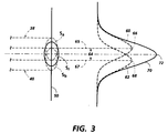
- FIG 3 there is shown a magnified portion of Figure 2 in which the two light beams 38 and 40 each individually generate a spot in the absence of the other beam.
- the light beams 38 and 40 individually strike the photoreceptor plane 50, they individually generate spots S a and S b respectively.
- the two light beams overlap, in effect they become one light beam which hereinafter it will be called “resulting light beam”.
- the resulting light beam strikes a plane, it generates one spot which hereinafter it will be called “resulting spot”.
- the size of the resulting spot S r is substantially equal to the size of the spot S a or S b generated by a single beam 38 or 40 respectively at its maximum intensity.
- Figure 3 also shows two Gaussian distributions 60 and 62 corresponding to two light beams 38 and 40 respectively along with the Gaussian distribution 70 of the resulting beam. If the two light beams 38 and 40 partially overlap in such a manner that the distance 64 between the peak 66 of the Gaussian distribution 60 and the peak 68 of the Gaussian distribution 62 is equal to Full Width Half Max of a single light beam at its maximum intensity divided by 2 (FWHM/2), then the resulting light beam will have a substantially Gaussian distribution 70.
- Full width half max (hereinafter referred to as "FWHM") is the width of the Gaussian distribution at half of the maximum intensity.
- spot separation the distance between the two peaks of the Gaussian distributions of the two light beams will be called "spot separation".
- the resulting spot S r will have a center at the mid point between the two center rays 65 and 67 of the two light beams 38 and 40 respectively. However, if the intensities of the two light beams are different, the center of the resulting spot S r will be closer to the center ray of the light beam with the higher intensity. The distance between the center of the resulting spot and the center ray of the light beam with the higher intensity depends on the difference between the two intensities of the two light beams.
- the effective spot size is equal to FWHM.
- the distance between the peak of the two light beams is equal to FWHM/2 of a single beam with maximum intensity
- the resulting light beam will have a spot size equal to the spot size (FWHM) of a single light beam with maximum intensity.
- the sum of the intensities of the two light beams should be kept equal to the maximum intensity of a single light beam.
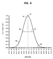
- FIGs 4 through 8 there are shown different examples of combining two light beams 38 and 40 of Figures 2 and 3 with different intensities.
- the horizontal axes represent the position of light beams and the vertical axes represent the intensity of the light beams.
- the Gaussian distributions 60, 62 and 70 correspond to the light beam 38, light beam 40 and the resulting light beam respectively.
- the light beam 38 has 50% of its maximum intensity and the light beam 40 has 50% its maximum intensity.
- the center C of the resulting spot S r is at the mid point between the two center rays 65 and 67 of the light beams 38 and 40 respectively.
- the light beam 38 has 75% of its maximum intensity and the light beam 40 has 25% of its maximum intensity.
- the resulting light beam will have a higher intensity than the intensity of the individual light beams 38 and 40.
- the resulting spot S r will have a center C closer to the center ray 65 of the light beam 38 which has higher intensity. Comparing Figures 4 and 5, it can be observed that by changing the intensity of the two combined light beams 38 and 40 the resulting spot has moved to a location closer to the light beam 38 with higher intensity.
- the Gaussian distribution 60 of the light beam 38 is shown with full intensity and the Gaussian distribution 62 of the light beam 40 is shown with zero intensity meaning that the light beam 40 is turned OFF.
- the Gaussian distribution 70 of the resulting light beam will be the same as the Gaussian distribution 60 of the light beam 38.
- the spot S a generated by the light beam 38 will be the resulting spot S r .
- the light beam 38 has 25% of its maximum intensity and the light beam 40 has 75% of its maximum intensity.
- the resulting light beam will have a higher intensity than the intensity of the individual light beams 38 and 40.
- the resulting spot S r will have a center C closer to the center ray 67 of the light beam 40 which has higher intensity. Comparing Figures 4 and 7, it can be observed that by changing the intensity of the two combined light beams 38 and 40 ( Figure 3) the resulting spot has moved to a location closer to the light beam 40 with higher intensity.
- the light beam 40 has full intensity and the light beam 38 has zero intensity meaning that the light beam 38 is turned OFF.
- the Gaussian distribution 70 of the resulting light beam will be the same as the Gaussian distribution 60 of the light beam 38.
- the spot S b generated by the light beam 40 will be the resulting spot S r .
- the size of the resulting spot S r is substantially equal to the size of a spot generated by a single light beam such as S a or S b (FWHM) at its maximum intensity. Also, it should be noted that the spot size on the Gaussian distribution of the resulting light beam is shown on the 0.5 line which is where the spot size of the single light beam with a maximum intensity is shown.
- the concept of combining two light beams can be utilized to correct a wobble in a raster scanner system.
- the resulting scan line can be moved to substantially reduce the wobble.
- the beams are not combined and one beam will always follow the other beam.
- the two paths that the two light beams scan partially overlap each other and therefore the result on the photoreceptor plane will be as if the two light beams were combined to scan one line.
- a raster scanner with wobble correcting optics which partially corrects the wobble can utilize a dual beam laser diode to further correct the partially corrected wobble.
- the 1/2 pixel limit on the wobble correction is based on using only two diodes. However, if more than 1/2 pixel wobble correction is needed, more diodes can be utilized to generate more light beams in which for any given scan line either one diode or only two diodes will be on to generate two light beams which scan two partially overlapping paths. The design and the operation of multiple diodes will be discussed further on.
- FIG. 9, 10 and 11 there are shown a front view of a laser light source 80 with two diodes D1 and D2, a perspective view of the light source 80 which generates two spots S1 and S2 on a photoreceptor plane 82 and a front view of the photoreceptor plane 82 respectively.
- the optical elements between the diodes D1 and D2 and the photoreceptor plane 82 are not shown.
- the two diodes D1 and D2 are located on a vertical axis 84.
- the two diodes D1 and D2 generate two light beams 86 and 88 and the two light beams 86 and 88 generate the two spots S1 and S2 on the photoreceptor plane 82.
- the two spots scan two different paths 89 and 92 without overlapping each other. Therefore, since the two paths 89 and 92 do not overlap, the positions of the two diodes D1 and D2 shown in Figures 9 and 10 are not appropriate positions for combining two light beams.
- FIGs 12, 13 and 14 are the same views as Figures 9, 10 and 11 respectively with different diode positions.
- the diodes D1 and D2 are placed side by side on a horizontal axis 90 which is also in the direction of the scan.
- the diodes D1 and D2 generate two spots S1 and S2 on the photoreceptor plane 82.
- the spot S2 follows the spot S1 and both spots scan the path 89. Since the two spots S1 and S2 scan the same path, the positions of the two diodes shown in Figures 12 and 13 are not appropriate positions for combing two light beams.
- the diodes D1 and D2 are placed in an offset position relative to each other in such a manner that the centers of the two diodes D1 and D2 are placed on a line 91 which is at an angle to the direction of scan 90.
- the position of the line 91 is dependent on the required spacing between the centers of the two diodes D1 and D2 and the amount of required overlap between the two generated spots S1 and S2.
- the diode pitch 93 which is the vertical distance between the two diodes D1 and D2 is selected to be FWHM/2 at the diode which provides a resulting spot with a substantially Gaussian intensity distribution.
- FWHM/2 at the diode is to distinguish it as being smaller than the FWHM/2 of the spot at the photoreceptor plane. It is also noted that the light beam's FWHM/2 at the diode, hereinafter referred to as the diode size, is smaller than the diode itself.
- spot S1 scans path 94 and spot S2 scans path 96 while following the spot S1. It can also be observed that the two paths 94 and 96 overlap each other over path 98. Since the scanning path of the two spots S1 and S2 partially overlap each other, the diode arrangement of Figure 15 is suitable for combining two light beams.
- the purpose of combining two light beams is to create one resulting spot which will apply one pixel onto the scan line. Therefore, the two light beams should receive the same pixel information and they should apply the pixel information onto the path in such a manner that each pixel from the top path should overlap the corresponding pixel from the bottom path to have the effect of one pixel in order to generate one scan line.
- FIG 18 there is shown a magnified view of Figure 17 while for simplicity the two paths 96 and 94 of Figure 17 are shown by two dashed lines 96 and 94 and the space between the spots is shown with a smaller space.
- position 100 is the position that the leading spot S1 applies the pixel information onto the path.
- a delay by any well known means can be applied to the driver of the diode D2.
- a delay on diode D2 will cause the modulation of the pixel information onto the light beam of the diode D2 to be delayed.
- the modulation of the pixel information onto the light beam of the diode D1 starts first and spot S1 starts to apply the pixel information from position 100 and moves on. After a delay of d in which, the spot S2 reaches the position 100, the modulation of the pixel information onto the light beam of the diode D2 starts. Therefore, the spot S2 also applies the pixel information onto the path at position 100.
- the modulation of the pixel information onto the light beam of diode D1 will be turned OFF and the spot S2 will move on until it reaches the end of scan 104 (a time delay equal to delay d) and then the modulation of the pixel information onto the light beam of diode D2 will be turned OFF.
- the amount of delay d depends on the distance between the centers of the two diodes D1 and D2 which is dependent on the required spacing between the diodes D1 and D2 that is set by the fabrication parameters. With a proper delay, the diode D2 will be delayed in such a manner that the generated spots S1 and S2 from the two diodes D1 and D2 both start applying the pixel information from a same starting point 100 and they both end applying the pixel information at the same ending point 104.
- FIG 19 there is shown a photoreceptor plane with two spots S1 and S2 which scan two paths that partially overlap each other.
- the path that spot S1 scans is shown by a dashed line 110 passing through the center of the spot S1 and the path that spot S2 scans is shown by dashed line 112 passing through the center of spot S2.
- dashed line 112 passing through the center of spot S2.
- the two spots S1 and S2 are combined the resulting spot scans a path or a line shown by phantom line 114.
- the intensity of the two light beams 86 and 88 ( Figure 16) generating the two spots S1 and S2 can be modified to move the resulting spot and therefore move the scan line 114 in the range between the centers of the two spots (spot separation 116).
- FIG. 20 there are shown an arrangement of a multi-diode laser light source 118, a perspective view of the light source 118 with five diodes D1, D2, D3, D4 and D5 which generates five spots S1, S2, S3, S4 and S5 on a photoreceptor plane 82 and a front view of the photoreceptor plane 82 respectively.
- the optical elements between the laser light source 118 and the photoreceptor plane 82 are not shown.
- the D1, D2, D3, D4 and D5 are placed in an offset position relative to each other in such a manner that the centers of all the diodes are on line 91 which is at an angle to the direction of scan 90.
- the position of line 91 is dependent on the required spacing between the centers of the diodes and the amount of overlap between the spots. In this arrangement, depending on the amount of the wobble, either one or two adjacent diodes will be selected to scan a line.
- the position 100 ( Figure 22), which is the start of the scan for the spot S1, is considered to be the start of the scan for all the scan lines.
- the diodes D2, D3, D4 and D5 ( Figure 20) should be delayed by d1, d2, d3 and d4 ( Figure 22) respectively. With these delays, selection of any adjacent two diodes will generate a scan line which starts at position 100 ( Figure 22).
- both diodes D2 and D3 generate two spots which scan two paths with a starting point at position 100 ( Figure 22).
- both diodes D4 and D5 generate two spots which scan two paths with a starting point at position 100 ( Figure 22).
- FIG 23 there is shown a magnified view of multi-diode laser light source 121.
- the diodes are staggered to provide an arrangement which needs less number of delays compared to the number of delays used in the embodiment of Figure 15.
- the diodes D1, D2 and D3 are placed on line 135 which is at an angle to the direction of the scan 90, the diodes D4, D5 and D6 are placed on line 137 and the diodes D7, D8 and D9 are placed on line 139.
- the lines 137 and 139 are parallel to line 135.
- the number of required columns depend on the diode spacing 124 (the distance between the centers of the two diodes). Depending on the requirements of the fabrication technology, the diode spacing 124 may have some restrictions.
- the space 124 between the two diodes D1 and D4 on column 84 is large. Therefore, the two diodes can not produce two spots which can scan two partially overlapping paths.
- the diodes on the columns 130 and 132 are added to fill the gap between the diodes on column 84.
- the diodes that follow each other on the path 133 are offset relative to each other with respect to the direction of scan. Also, only the diodes that follow each other on the path 133 can be selected to generate two spots which can scan two partially overlapping paths. For example, D1 and D2, D2 and D3 or D3 and D4 can be selected as a designated diode pair.
- the diode arrangement of Figure 23 generates the spots S1, S2, S3, S4, S5, S6, S7, S8 and S9 shown in Figure 24.
- the diodes on column 130 should be delayed by d1 and the diodes on column 132 should be delayed by d2.
- the diode separation distance 124 between the two diodes D1 and D4 on the vertical axis 84, has to be defined.
- This distance 124 is the required distance between the diodes which is defined by the technology.
- the diode pitch 126 which is the vertical distance between the two centers of any two diodes which follow each other on the path 133, has to be defined.
- the pitch 126 is equal to the light beam's FWHM/2 at the diode which permits the generation of two spots which can scan two partially overlapping paths.
- the number of the required columns has to be determined.
- the preferred embodiment of this invention utilizes a vertical cavity surface emitting laser (VCSEL) or other surface emitting laser array.
- VCSEL vertical cavity surface emitting laser
- the advantage of utilizing a VCSEL array is that the light beam, generated by each diode on the VCSEL array, is substantially collimated and therefore it produces a circular spot compared to the edge emitting diode arrays which generate an elliptical spot.
- the edge emitting diode arrays can also be utilized to combine the light beams and the shapes of the spots can be modified, by well known methods to be substantially circular.
- the spot separation has to be FWHM/2 of a single light beam with its maximum intensity which generates a resulting spot with a substantially Gaussian distribution.
- different spot separations may be utilized which will provide a resulting spot with an intensity distribution other than Gaussian distribution.
- the aforementioned embodiment discloses different diode arrangements to combine two light beams.
- it is necessary to detect the position of the spots generated by the diode arrangement in comparison with the correct position of the scan line. Once the position of the spots are detected, then a proper pair of diodes can be selected to be the designated diode pair for that scan line. Also, based on the position of diodes and the position of the scan line, the intensities of the two light beams generated by the designated pair of diodes can be modified to achieve fine alignments between the two light beams and the scan line.
- a position detector 140 In order to detect the position of the spots compared to the scan line a position detector can be utilized. Referring to Figure 25, there is shown a position detector 140.
- the position detector 140 has two elements 142 and 144.
- the two elements 142 and 144 can each have a triangular shape, a trapezoidal shape or any other shape with the following relationships.
- the two elements are placed adjacent to each other in such a manner that on a reference axis 146, the width of both elements are equal.
- the edge 141 of element 142 is parallel to edge 143 of the element 144. So, each element will have a varying distance between its edges scanned by a spot and such distance on one element will be different than corresponding distance on the other element except at the reference axis.
- edge 145 of element 142 is adjacent to and spaced from edge 147 of the element 144 and there edges are parallel to each other. Also, the edges 145 and 147, separating the two elements 142 and 144, must be orthogonal to the scan direction 152 to also use the crossing of the edges by a spot as a start of scan detector. This crossing will be a constant reference point in the direction of scan irrespective of the position of the spot relative to the reference axis 146.
- the position detector 140 To detect the position of the spots relative to the reference axis 146, the position detector 140 will be placed just prior to the edge of a paper under print and the spot S1 from diode D1 of any diode design will be arranged to cross the detector 140 on the reference axis 146. However, the position of the middle spot S3 is the correct position of the scan line 152. The reason for sending the spot S1 to the detector 140 is that the spot S1 is the first spot that reaches the detector 140. It should be noted that while the spot S1 is crossing the detector 140, the rest of the diodes are turned OFF.
- the position detector 140 will be placed just prior to the edge of a paper under print in such a manner that the space 150 between the two elements 142 and 144 will be coincident with the start of the scan.
- the spot S1 crosses the position detector 140 above the reference axis 146, it crosses the first element 142 at the narrower area and it crosses the second element 144 at a wider area. Therefore, the first element measures a shorter distance and the second element measures a longer distance.
- the spot S1 crosses the position detector 140 below the reference axis 146, it crosses the first element 142 at the wider area and it crosses the second element 144 at a narrower area. Therefore, the first element measures a longer distance and the second element measures a shorter distance and if the spot S1 crosses the position detector 140 on the reference axis 146, the two elements 142 and 144 measure equal distances.
- the position of the middle spot is the correct position of the scan line and therefore the middle spot should be selected to scan the line.
- the position of the spot S3 which is the middle spot is the correct position of the scan and therefore, the diode D3 (not shown) which generates the spot S3 should be selected to be the designated diode.
- the spot S1 crosses the position detector below the reference axis of the 146, it means that the middle spot is below the scan line and therefore there is a wobble on that scan line.
- two spots from the group of spots including the middle spot and spots above the middle spot (S3, S4 and S5) or one spot from the group of spots above the middle spot (S4 and S5) will be selected to be the designated spots or spot to scan that line.
- the diodes or the diode generating those spots or spot will be the designated diodes or diode.
- the intensities of the two spots can be modified to achieve the fine alignment between the two spots and the scan line.
- the spot S1 crosses the position detector above the reference axis 146, it means that the middle spot is above the scan line and therefore there is a wobble on that scan line.
- two spots from the group of spots including the middle spot and spots below the middle spot (S3, S2 and S1) or one spot from the group of spots below the middle spot (S2 and S1) will be selected to be the designated spots or spot to scan that line.
- the diodes or the diode generating those spots or spot will be the designated diodes or diode.
- the intensities of the two spots can be modified to achieve the fine alignment between the two spots and the scan line.
- the position of the resulting spot from the combination of the two middle light beams, each with 50% of its maximum intensity, will be the correct position of the scan line.
- FIG. 26 and 27 there is shown a controlling circuit diagram for one of the diode arrangements ( Figure 20) of this invention which is utilized to correct the wobble on different scan lines.
- the circuit shown in Figures 26 and 27 is designed by the well known means.
- diode D1 (not shown) will be turned on and the spot S1 generated by the diode D1 will be sent to the position detector 140.
- the spot S1 starts crossing each element of the position detector, the element generates a voltage and when the spot generated by the light beam is completely on the element, the element generates the maximum voltage Vm.
- the voltage generated by the element 142 is being compared to a reference voltage equal to Vm/2 (which represents a voltage generated by the element when the spot is half way on the element) by a comparator C1.
- the element 142 when the spot S1 starts crossing the element 142, the element 142 generates a voltage and when this voltage reaches Vm/2, the comparator C1 switches and turns ON the up/down counter 160.
- the element 142 also generates a signal which through comparator C3 sends a signal to the up/down counter 160 causing the up/down counter 160 to start counting up. While the up/down counter 160 is counting up, it measures the distance which is travelled by the light beam (spot S1) from edge 141 to edge 145 ( Figure 25) of element 142.
- the comparator C3 which compares the voltage generated by the element 142 with the voltage generated by the element 144, switches. When the comparator C3 switches, it indicates the start of the scan.
- the start of scan signal generated by C3 is also used to flag the up/down counter 160 to start counting down. While the up/down counter 160 is counting down, it measures the distance which is travelled by the light beam (spot S1) from edge 147 to edge 143 of element 144. The up/down counter 160 stops counting when the spot S1 exits the element 144.
- the spot S1 may cross the optical element 142 in a narrower or a wider area than the area of the element 144. This will cause a different count while the spot S1 crosses each element.
- the up/down counter 160 which counts up for the element 142 and count down for element 144, will have a zero count when the spot S1 exits the element 144.
- the resulting count from the up/down counter 160 is sent to two programmable logic arrays (PLA) 162 and 164.
- PLA programmable logic arrays
- the PLA 162 provides the proper intensities
- PLA 164 provides the proper selection of the diodes.
- a digital to analog converter 166 converts the digital intensity signal for the selected one diode into an analog signal I1 or I2 depending on the selected diode or it converts the two digital intensity signals for the two selected offset diodes into two analog signals I1 and I2, one for each of the two light beams that will be generated.
- the current amplifier 168 amplifies the current signal I1 and the current amplifier 170 amplifies the current signal I2.
- the switches Q10 through Q17 will turn ON the proper diodes D1 through D5 and activate the modulating switches Q18 through Q22.
- the switches Q18 through Q22 are responsible for modulating the pixel information onto the light beam generated by the diodes D1 through D5.
- the delays d1, d2, d3 and d4 are responsible to apply a proper delay to the pixel information of each diode before modulation.
- circuit shown in Figures 26 and 27 can be designed in many different ways with different number of diodes.
- the position detector of this invention in conjunction with any diode design disclosed in the various embodiments of this invention provide a system which can correct the wobble of a scanning system.
- the disclosed embodiments of this invention are capable of correcting any wobble within any range, the conventional wobble correcting optics will no longer be needed.
- the conventional wobble correcting optics are the only optical elements which require cylindrical lenses. Therefore, by eliminating the conventional wobble correcting optics, the cylindrical lenses utilized in a raster scanner for correcting wobble will be eliminated.
- a raster scanning system can also utilize different embodiments of this invention to correct a bow of a scan line.
- a bow of a scan line during assembly, the position of each pixel (i.e pixel P3 or P4) on a bowed scan line 174 relative to a straight scan line 176 will be measured and based on the measured data from each pixel, the required correction will be defined which then the correction data will be stored in a memory. Once the correction data is stored, every time it is needed to modulate a pixel onto the light beam, the correction data for that pixel will be retrieved and based on the required correction for that pixel, either a single diode or a proper pair of diodes with proper intensities will be selected. With this approach a bow of a scan line can be substantially reduced.
- FIG. 29 there is shown a controlling circuit diagram for one of the diode arrangements ( Figure 20) of this invention which is utilized to correct the bow of a scan line.
- the position detector 140 will be used to indicate the start of the scan.
- the comparator C3 changes state which provides the start of the scan.
- a counter 180 starts counting until it counts to the position in which the pixel information should be applied to the scan line. Any count beyond the position in which the pixel information should be applied to the scan line will be called pixel count.
- the counts from the counter 180 are sent to a ROM 182.
- the ROM 182 is programmed to provide the proper intensities and diode selection for each pixel.
- the counter 180 indicates the pixel count and the pixel count addresses the ROM 182 to send out the diode selection and the intensity values.
- the output of the ROM 182 will be sent out to digital to analog convertors DAC1, DAC2, DAC3, DAC4 and DAC5. Only the selected DACs which receive a value from the ROM 182, convert the digital intensity values to analog intensity values.
- the analog intensity values from the selected DACs will activate the corresponding voltage controller current sources 186, 188, 190, 192 and 194.
- the activated voltage controller current sources will provide proper currents to corresponding laser diodes D1, D2, D3, D4 and D5 to emit light beams with the required intensities.
Landscapes
- Engineering & Computer Science (AREA)
- Physics & Mathematics (AREA)
- Optics & Photonics (AREA)
- General Engineering & Computer Science (AREA)
- General Physics & Mathematics (AREA)
- Theoretical Computer Science (AREA)
- Multimedia (AREA)
- Signal Processing (AREA)
- Mechanical Optical Scanning Systems (AREA)
- Facsimile Scanning Arrangements (AREA)
Applications Claiming Priority (2)
| Application Number | Priority Date | Filing Date | Title |
|---|---|---|---|
| US13058093A | 1993-10-01 | 1993-10-01 | |
| US130580 | 1993-10-01 |
Publications (3)
| Publication Number | Publication Date |
|---|---|
| EP0659011A2 true EP0659011A2 (de) | 1995-06-21 |
| EP0659011A3 EP0659011A3 (de) | 1996-01-17 |
| EP0659011B1 EP0659011B1 (de) | 1999-12-08 |
Family
ID=22445351
Family Applications (1)
| Application Number | Title | Priority Date | Filing Date |
|---|---|---|---|
| EP94307160A Expired - Lifetime EP0659011B1 (de) | 1993-10-01 | 1994-09-30 | Schwankungs- und Bogenkorrektur durch Intensitätsproportionierung von mehreren Bildelementpunkten |
Country Status (4)
| Country | Link |
|---|---|
| US (1) | US5517328A (de) |
| EP (1) | EP0659011B1 (de) |
| JP (1) | JPH07174995A (de) |
| DE (1) | DE69422007T2 (de) |
Cited By (2)
| Publication number | Priority date | Publication date | Assignee | Title |
|---|---|---|---|---|
| WO2005114977A1 (en) * | 2004-05-19 | 2005-12-01 | Intense Limited | Thermal printing with laser activation |
| WO2007105329A1 (en) * | 2006-03-10 | 2007-09-20 | Ricoh Company, Ltd. | Light scanning apparatus, light scanning method, image forming apparatus, color image forming apparatus, and recording medium having program |
Families Citing this family (20)
| Publication number | Priority date | Publication date | Assignee | Title |
|---|---|---|---|---|
| US5973709A (en) * | 1992-06-24 | 1999-10-26 | Oki Electric Industry Co., Ltd. | Printer and process for printing different size dots by setting drive energies based on adjacent data bit logic |
| JP2912556B2 (ja) * | 1994-10-25 | 1999-06-28 | 富士通株式会社 | 像形成装置における露光方法及び像形成装置 |
| US5745152A (en) * | 1994-10-31 | 1998-04-28 | Hewlett Packard Company | Multiple beam laser scanner using lasers with different aperture sizes |
| US5940113A (en) * | 1994-12-19 | 1999-08-17 | Xerox Corporation | Lensless printing system with a light bar printhead |
| US6044096A (en) * | 1997-11-03 | 2000-03-28 | Sdl, Inc. | Packaged laser diode array system and method with reduced asymmetry |
| US5933682A (en) * | 1998-04-14 | 1999-08-03 | Eastman Kodak Company | Copier/printer with manual adjustment for cross-track uniformity |
| JP2000227564A (ja) * | 1999-02-05 | 2000-08-15 | Minolta Co Ltd | マルチビーム走査光学装置 |
| US6229555B1 (en) * | 2000-05-17 | 2001-05-08 | Lexmark International, Inc. | Method and apparatus for minimizing visual artifacts generated by an electrophotographic machine during imaging |
| JP3600228B2 (ja) * | 2002-03-01 | 2004-12-15 | 株式会社リコー | 光走査装置および画像形成装置 |
| US7349123B2 (en) * | 2004-03-24 | 2008-03-25 | Lexmark International, Inc. | Algorithms and methods for determining laser beam process direction position errors from data stored on a printhead |
| US7375738B2 (en) * | 2004-03-24 | 2008-05-20 | Lexmark International, Inc. | Electronic systems and methods for reducing laser beam process direction position errors |
| JP2006159647A (ja) | 2004-12-07 | 2006-06-22 | Canon Inc | 画像形成装置及びその方法 |
| US7271821B2 (en) * | 2004-12-16 | 2007-09-18 | Marvell International Technology Ltd. | Laser printer with reduced banding artifacts |
| JP2007047644A (ja) * | 2005-08-12 | 2007-02-22 | Ricoh Co Ltd | 光走査装置及び画像形成装置 |
| JP2007148346A (ja) * | 2005-10-25 | 2007-06-14 | Ricoh Co Ltd | 光走査装置及び画像形成装置 |
| KR100739761B1 (ko) * | 2005-11-23 | 2007-07-13 | 삼성전자주식회사 | 멀티 빔 주사장치 |
| JP4896663B2 (ja) * | 2006-02-17 | 2012-03-14 | 株式会社リコー | 画素形成装置、光走査装置、光走査方法、画像形成装置、カラー画像形成装置、プログラム、記録媒体 |
| US8253768B2 (en) | 2005-12-09 | 2012-08-28 | Ricoh Company, Ltd. | Optical scanner and image forming apparatus |
| JP4863840B2 (ja) * | 2006-10-27 | 2012-01-25 | 株式会社リコー | 画素形成装置、光走査装置、光走査方法、画像形成装置、カラー画像形成装置 |
| JP2008209675A (ja) * | 2007-02-27 | 2008-09-11 | Ricoh Co Ltd | 光走査装置及び画像形成装置 |
Citations (2)
| Publication number | Priority date | Publication date | Assignee | Title |
|---|---|---|---|---|
| US4864326A (en) * | 1985-03-18 | 1989-09-05 | Canon Kabushiki Kaisha | Dual beam recorder |
| EP0549204A1 (de) * | 1991-12-20 | 1993-06-30 | Xerox Corporation | Kontrolle der Strahlposition für ein Abtastgerät |
Family Cites Families (12)
| Publication number | Priority date | Publication date | Assignee | Title |
|---|---|---|---|---|
| US4639608A (en) * | 1983-05-18 | 1987-01-27 | Canon Kabushiki Kaisha | Image read-out apparatus with light source driving means |
| JPS60197063A (ja) * | 1984-03-21 | 1985-10-05 | Canon Inc | Ledアレイ及びその分割点灯方法 |
| JPH059704Y2 (de) * | 1987-12-11 | 1993-03-10 | ||
| DE68924286T2 (de) * | 1988-02-18 | 1996-02-29 | Fuji Photo Film Co Ltd | Verfahren und Apparat zum Lesen und zur Reproduktion von Bildern und Lichtquelleneinrichtung mehrerer Halbleiterlaser dazu. |
| JPH02109013A (ja) * | 1988-10-19 | 1990-04-20 | Hitachi Koki Co Ltd | 光走査装置 |
| US5212569A (en) * | 1989-06-29 | 1993-05-18 | Fuji Photo Film Co., Ltd. | Light beam scanning apparatus capable of changing the scanning density |
| US5023448A (en) * | 1989-10-16 | 1991-06-11 | Eastman Kodak Company | Beam position sensor for a light beam scanner |
| US5151586A (en) * | 1990-08-01 | 1992-09-29 | Brother Kogyo Kabushiki Kaisha | Scanning exposure device provided with intensity correction to compensate for scan angle |
| US5165074A (en) * | 1990-08-20 | 1992-11-17 | Xerox Corporation | Means and method for controlling raster output scanner intensity |
| DE69123923T2 (de) * | 1990-10-12 | 1997-04-30 | Fuji Photo Film Co Ltd | Abtast- und Beleuchtungsverfahren mit mehreren optischen Strahlen und Vorrichtung dazu |
| US5204523A (en) * | 1991-08-19 | 1993-04-20 | Xerox Corporation | Method for spot position control in an optical output device employing a variable wavelength light source and an optical beam deflecting element |
| US5212381A (en) * | 1991-08-19 | 1993-05-18 | Xerox Corporation | Method of controlling slow scan direction of spot position in an optical output device employing an electro-optical control apparatus |
-
1994
- 1994-09-26 JP JP6229879A patent/JPH07174995A/ja active Pending
- 1994-09-30 DE DE69422007T patent/DE69422007T2/de not_active Expired - Fee Related
- 1994-09-30 EP EP94307160A patent/EP0659011B1/de not_active Expired - Lifetime
-
1995
- 1995-02-16 US US08/389,447 patent/US5517328A/en not_active Expired - Lifetime
Patent Citations (2)
| Publication number | Priority date | Publication date | Assignee | Title |
|---|---|---|---|---|
| US4864326A (en) * | 1985-03-18 | 1989-09-05 | Canon Kabushiki Kaisha | Dual beam recorder |
| EP0549204A1 (de) * | 1991-12-20 | 1993-06-30 | Xerox Corporation | Kontrolle der Strahlposition für ein Abtastgerät |
Non-Patent Citations (1)
| Title |
|---|
| XEROX DISCLOSURE JOURNAL, vol. 17, no. 5, 31 October 1992 STAMFORD US, pages 393-399, XP 000316000 F.C. GENOVESE 'Multiple-spot beam control for a raster output scanner' * |
Cited By (5)
| Publication number | Priority date | Publication date | Assignee | Title |
|---|---|---|---|---|
| WO2005114977A1 (en) * | 2004-05-19 | 2005-12-01 | Intense Limited | Thermal printing with laser activation |
| WO2007105329A1 (en) * | 2006-03-10 | 2007-09-20 | Ricoh Company, Ltd. | Light scanning apparatus, light scanning method, image forming apparatus, color image forming apparatus, and recording medium having program |
| CN101193755B (zh) * | 2006-03-10 | 2011-06-15 | 株式会社理光 | 光扫描装置及方法、图像形成装置、彩色图像形成装置 |
| US8310516B2 (en) | 2006-03-10 | 2012-11-13 | Ricoh Company, Ltd. | Light scanning apparatus, light scanning method, image forming apparatus, color image forming apparatus, and recording medium having program |
| EP1993843A4 (de) * | 2006-03-10 | 2015-10-14 | Ricoh Co Ltd | Lichterfassungsvorrichtung, lichterfassungsverfahren, bilderzeugungsvorrichtung, bildfarbenerzeugungsvorrichtung und aufzeichnungsmedium mit dem programm |
Also Published As
| Publication number | Publication date |
|---|---|
| DE69422007D1 (de) | 2000-01-13 |
| DE69422007T2 (de) | 2000-05-25 |
| US5517328A (en) | 1996-05-14 |
| JPH07174995A (ja) | 1995-07-14 |
| EP0659011A3 (de) | 1996-01-17 |
| EP0659011B1 (de) | 1999-12-08 |
Similar Documents
| Publication | Publication Date | Title |
|---|---|---|
| US5517328A (en) | Wobble and bow correction by dual spot pixel intensity proportioning | |
| US8005321B2 (en) | Pixel clock generator, optical scanner, and image forming apparatus | |
| US20040125199A1 (en) | Pixel clock generation apparatus, pixel clock generation method, and image forming apparatus capable of correcting main scan dot position shift with a high degree of accuracy | |
| US5930019A (en) | Light scanning device, optical device, and scanning method of optical device | |
| JP4868841B2 (ja) | 光走査装置及び画像形成装置 | |
| EP1111435B1 (de) | Optischer Rasterabtaster mit reduzierter Bauhöhe erreicht durch mehrere Schwankungskorrekturelemente | |
| US5526166A (en) | Optical system for the correction of differential scanline bow | |
| US5589870A (en) | Spot profile control using fractional interlace factors in a polygon ROS | |
| US5357106A (en) | Sensor for detecting beam position and start of scan position | |
| EP0605131B1 (de) | Verfahren und Gerät zur Störungsbeseitigung durch überabgetastete Beleuchtung für optische Drucker und ähnliche mit photoempfindlichem Aufzeichnungsmedium mit hohem Gamma und hoher Adressierbarkeit | |
| US20040160516A1 (en) | Light beam display employing polygon scan optics with parallel scan lines | |
| JPH0876039A (ja) | マルチビームレーザ記録装置 | |
| US5550668A (en) | Multispot polygon ROS with maximized line separation depth of focus | |
| EP0596719B1 (de) | Schnelle Abtastspotkorrektur mit Pulsbreitenmodulator in einem Rasterabtastpolygon | |
| US5617133A (en) | Method and apparatus for adjusting orientation of light beams in a raster scanning system | |
| US7379085B2 (en) | System and method for reducing non-linearity errors between two imaging stations | |
| US5247373A (en) | Scanning optical system | |
| JP3291341B2 (ja) | スポット位置制御装置 | |
| JP3705633B2 (ja) | ラスタ出力スキャナにおける画素位置調節装置及び方法 | |
| JP2003276234A (ja) | 画像形成装置 | |
| JP2008026541A (ja) | 光ビーム走査装置 | |
| JPH09251137A (ja) | レーザ記録装置 | |
| EP0715197A2 (de) | Anamorphotisches Zoomlinsensystem zur Kontrolle des Abtastlinienabstandes | |
| JP5939822B2 (ja) | 光走査装置および画像形成装置 | |
| JP4298091B2 (ja) | 走査光学装置の組立方法 |
Legal Events
| Date | Code | Title | Description |
|---|---|---|---|
| PUAI | Public reference made under article 153(3) epc to a published international application that has entered the european phase |
Free format text: ORIGINAL CODE: 0009012 |
|
| AK | Designated contracting states |
Kind code of ref document: A2 Designated state(s): DE FR GB |
|
| PUAL | Search report despatched |
Free format text: ORIGINAL CODE: 0009013 |
|
| AK | Designated contracting states |
Kind code of ref document: A3 Designated state(s): DE FR GB |
|
| 17P | Request for examination filed |
Effective date: 19960717 |
|
| 17Q | First examination report despatched |
Effective date: 19980515 |
|
| GRAG | Despatch of communication of intention to grant |
Free format text: ORIGINAL CODE: EPIDOS AGRA |
|
| GRAG | Despatch of communication of intention to grant |
Free format text: ORIGINAL CODE: EPIDOS AGRA |
|
| GRAH | Despatch of communication of intention to grant a patent |
Free format text: ORIGINAL CODE: EPIDOS IGRA |
|
| GRAH | Despatch of communication of intention to grant a patent |
Free format text: ORIGINAL CODE: EPIDOS IGRA |
|
| GRAA | (expected) grant |
Free format text: ORIGINAL CODE: 0009210 |
|
| AK | Designated contracting states |
Kind code of ref document: B1 Designated state(s): DE FR GB |
|
| REF | Corresponds to: |
Ref document number: 69422007 Country of ref document: DE Date of ref document: 20000113 |
|
| ET | Fr: translation filed | ||
| PLBE | No opposition filed within time limit |
Free format text: ORIGINAL CODE: 0009261 |
|
| STAA | Information on the status of an ep patent application or granted ep patent |
Free format text: STATUS: NO OPPOSITION FILED WITHIN TIME LIMIT |
|
| 26N | No opposition filed | ||
| REG | Reference to a national code |
Ref country code: GB Ref legal event code: IF02 |
|
| PGFP | Annual fee paid to national office [announced via postgrant information from national office to epo] |
Ref country code: FR Payment date: 20020910 Year of fee payment: 9 |
|
| PGFP | Annual fee paid to national office [announced via postgrant information from national office to epo] |
Ref country code: GB Payment date: 20020925 Year of fee payment: 9 |
|
| PGFP | Annual fee paid to national office [announced via postgrant information from national office to epo] |
Ref country code: DE Payment date: 20021011 Year of fee payment: 9 |
|
| PG25 | Lapsed in a contracting state [announced via postgrant information from national office to epo] |
Ref country code: GB Free format text: LAPSE BECAUSE OF NON-PAYMENT OF DUE FEES Effective date: 20030930 |
|
| PG25 | Lapsed in a contracting state [announced via postgrant information from national office to epo] |
Ref country code: DE Free format text: LAPSE BECAUSE OF NON-PAYMENT OF DUE FEES Effective date: 20040401 |
|
| GBPC | Gb: european patent ceased through non-payment of renewal fee |
Effective date: 20030930 |
|
| PG25 | Lapsed in a contracting state [announced via postgrant information from national office to epo] |
Ref country code: FR Free format text: LAPSE BECAUSE OF NON-PAYMENT OF DUE FEES Effective date: 20040528 |
|
| REG | Reference to a national code |
Ref country code: FR Ref legal event code: ST |