EP0657892A2 - Speicheranordnung mit asymmetrischer Bildung zwischen CAS und Daten-Ein/Ausgang und Anwendungen davon - Google Patents
Speicheranordnung mit asymmetrischer Bildung zwischen CAS und Daten-Ein/Ausgang und Anwendungen davon Download PDFInfo
- Publication number
- EP0657892A2 EP0657892A2 EP94116320A EP94116320A EP0657892A2 EP 0657892 A2 EP0657892 A2 EP 0657892A2 EP 94116320 A EP94116320 A EP 94116320A EP 94116320 A EP94116320 A EP 94116320A EP 0657892 A2 EP0657892 A2 EP 0657892A2
- Authority
- EP
- European Patent Office
- Prior art keywords
- memory
- memory system
- data
- circuit means
- cells
- Prior art date
- Legal status (The legal status is an assumption and is not a legal conclusion. Google has not performed a legal analysis and makes no representation as to the accuracy of the status listed.)
- Withdrawn
Links
Images


Classifications
-
- G—PHYSICS
- G11—INFORMATION STORAGE
- G11C—STATIC STORES
- G11C7/00—Arrangements for writing information into, or reading information out from, a digital store
- G11C7/22—Read-write [R-W] timing or clocking circuits; Read-write [R-W] control signal generators or management
-
- G—PHYSICS
- G11—INFORMATION STORAGE
- G11C—STATIC STORES
- G11C7/00—Arrangements for writing information into, or reading information out from, a digital store
- G11C7/10—Input/output [I/O] data interface arrangements, e.g. I/O data control circuits, I/O data buffers
- G11C7/1006—Data managing, e.g. manipulating data before writing or reading out, data bus switches or control circuits therefor
Definitions
- the present invention relates to semiconductor memory array architectures in which a semiconductor memory array provides more than a single data bit for each chip access cycle, and more particularly to arrays in which subsets of data bits can be accessed independently.
- each succeeding generation of memory products contains four times the number of memory bits as the proceeding generation.
- DRAM Dynamic RAM
- Mb 1-Megabit
- 4Mb 4Mb
- 16Mb 16Mb
- 64Mb 64Mb
- Each generation strives to provide similar functions and organizational features as found in previous generations; however, the compatibility of addressing schemes has dictated that each suceeding generation of Random Access Memory (RAM) utilize additional address input signals to address the increasing number of memory cells found in each suceeding generation of memory devices.
- the additional address input signals act to increase the memory depth of the DRAM memory device.
- a 16Mb DRAM may be offered in organizations of 16MbX1, 4MbX4, 2MbX8, or even 1MbX16. (The "Xn” portion of such designation is recited as "by n", such as "by 1.")
- a X4 chip can be used to replace four X1 chips of the previous generation.
- error detection In high reliability systems it is preferred to utilize some sort of error detection with or with out error correction in conjunction with memory systems.
- the simplest way to implement error detection is to add a single "parity" bit to each byte which is a function of all of the bits in a byte.
- the additional bits require a memory system which can accommodate a nine bit byte organizations. This requirement has been met in the past by building the memory system out of multiples of nine X1 chips.
- X1 memory chips causes the total memory contained in the memory system to exceed the amount that can be practically used.
- a common feature of DRAM memory system organizations is that each nine bit byte can be independently accessible. Thus, even for memory systems which can concurrently provide 4 or 8 bytes of data, each byte must be addressable.
- the solution put forward by Neal and Poteet, uses a plurality of chips all of a common generation of technology, but requires two different memory chip architectures.
- a new chip design which has the density of 1Mb is organized as four separate 256KbX1 memories and is designated as Quad CAS.
- Each of the four memories on a chip is responsive to a different column address strobe (CAS) input (CAS1...CAS4) and each CASn selects one of four data input/output ports.
- CAS column address strobe
- the solution they describe is intended to work for a memory system which is comprised of a plurality of X4 chips.
- the solution uses one or more dedicated chips solely to provide the odd ninth data bit.
- a multi-bit data control function which enables independent control of at least a plurality of data bits via a single control signal.
- a logically organized memory chip is organized as a 2 N X4 chip in which one control (CAS0) signal enables a single data bit and another control (CAS1) signal enables the remaining three data bits.
- FIG. 1 there is shown a typical DRAM chip organization illustrating the application of the invention. Although a specific embodiment is shown, any matrix organized memory having at least four data input/output pads can be used to implement the invention. It should be understood the reference to data in and/or data out should be considered inclusive. The actual direction in which data is transferred is not relevant to the subject invention, as it is the control of specific data I/O lines that is significant.
- chip 10 is a 1Mb DRAM organized as 256KX4 and is responsive to address input signals applied to address inputs 12 in the conventional time division multiplexed manner.
- nine row addresses are applied to row address buffers 13 which apply signals to the two row decoder circuits 11a and 11b, which in turn select row lines in the memory sub-arrays 10a, 10b, 10c and 10d.
- nine column address signals are applied to column address buffers 15 which apply their output signals to a plurality of sense amplifiers, intermediate buffers and multiplexer 17 in order to enable the selection of four specific bits to be coupled through the data I/O buffers 18a - 18d.
- CAS column address strobe
- the data I/O buffers are strobed by a CAS signal allowing data to be input or output via one the four data pads DQ0, DQ1, DQ2 and DQ3.
- the externally applied CAS signals act as clocking signals to certain portions of the memory chip and are used to initiate internal clock and timing signals on memory chip.
- the data I/O buffers are strobed by a CAS signal allowing data to be input or output via one of the four data pads DQ1, DQ2, DQ3 and DQ4.
- the CAS0 signal is coupled to buffer 18a and controls data bit DQ1.
- the CAS1 signal is coupled to the three remaining buffers 18b, 18c and 18d and controls data bits DQ2, DQ3, and DQ4.
- one or two CAS signals can be present, depending on the organization of the data I/O pads of the chips and those of the SIMM. In the case where a single CAS signal is presnt during a memory cycle, either one or three data bits will be active. In the case where both CAS signals are present, all four bit will be active. To the extent that information is required to further illustrate the specific timing between the various signals applied to the DRAM chip, reference may be made to the above cited prior art patent, which is hereby incorporated by reference.
- Fig 2 illustrates a representative package for a 4Mb memory organized as 1MbX4 having the two CAS inputs of the same type as the device of Fig. 1.
- Fig. 3 illustrates an example of a four byte X36 parity 72 pin SIMM architecture using two different types of DRAM chips. Three of the chips are organized as X1 and X3 and the remaining chips are organized as X4 chips. Note that CAS0 controls two X4 chips and the X1 portion of a third chip. CAS1 controls three X3 portions of three chips. In addition, each CAS is aymmetrically balanced to drive three chips.
- FIG. 4 illustrates another embodiment of the invention as an 8 byte, 72 bit parity SIMM and is show implemented using 2 N X8 DRAM architecture using chips configured as 2 N X3 and 2 N X5 as well as 2 N X4 organizations. Combinations of three X3 chips and a X4 and a X5 chip are used to form the required 9-bit byte for each of eight CAS inputs.
- 8MbX3/8MbX5 and 8MbX4/8MbX4 can be used.
- Fig. 5 illustrates another memory system using the invnetion to create a four byte, 36 bit parity SIMM. It is shown implemented using 2 N X16 DRAM architecture using chips configured as 2 N X9/X2/X5 as well as 2 N X9 and X7 organizations and a 2 N X4 from a previous generation t form the required 9-bit byte for each of the four CAS inputs.
- chip architectures of 1MbX16 configures as 1MbX9/X2/X5 and 1MbX9/7 as well as a 1MbX4 from the previous generation can be used.
- Fig. 6 shows a modification of the data I/O circuits in the Chip of Fig.
- a mode control signal is provided to enable the control of one of the data I/O circuits such that when the mode control signal is in one state the output of logic gate 50 enables the data I/O for DQ1 to be responsive to the CAS0 clock signal.
- the DRAM chip operates as previously described.
- the mode control is in the opposite state, the data I/O for DQ1 is responsive to CAS1 and enables DQ1 at the same time as the remaining data I/O circuits.
- the chip responds as a X4 chip. Utilizing a mode control input allows the same chip part number to be utilized for all of the chips used in the SIMM of Fig. 3.
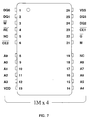
- a chip package pin out illustrating use of the Mode pin M is shown in Fig. 7.
- the desired mode control signal can easily be applied at the SIMM level by coupling the mode control pin M to a fixed voltage source.
- a characteristic of the invention is that in each multi-chip module (SIMM) there are configured chip architectures comprising multiples of odd data I/O combinations. This characteristic is required in order to provide the necessary 9-bit bytes for system use.
- a significant advantage of the invention is the fact that each chip is required to include a provision for only one extra, or two CAS inputs, thus allowing alternative packaging schemes to more suitably be designed.
- a problem in the Quad CAS solution is that three additional input pads are required to be dedicated to the additional CAS inputs for a "Quad CAS" design. Utilization of X8 "Octal CAS" adds a requirement for seven additional CAS input to each chip.
Applications Claiming Priority (2)
| Application Number | Priority Date | Filing Date | Title |
|---|---|---|---|
| US08/161,279 US5412613A (en) | 1993-12-06 | 1993-12-06 | Memory device having asymmetrical CAS to data input/output mapping and applications thereof |
| US161279 | 1993-12-06 |
Publications (2)
| Publication Number | Publication Date |
|---|---|
| EP0657892A2 true EP0657892A2 (de) | 1995-06-14 |
| EP0657892A3 EP0657892A3 (de) | 1996-01-17 |
Family
ID=22580562
Family Applications (1)
| Application Number | Title | Priority Date | Filing Date |
|---|---|---|---|
| EP94116320A Withdrawn EP0657892A3 (de) | 1993-12-06 | 1994-10-17 | Speicheranordnung mit asymmetrischer Bildung zwischen CAS und Daten-Ein/Ausgang und Anwendungen davon. |
Country Status (3)
| Country | Link |
|---|---|
| US (1) | US5412613A (de) |
| EP (1) | EP0657892A3 (de) |
| JP (1) | JP2688177B2 (de) |
Families Citing this family (18)
| Publication number | Priority date | Publication date | Assignee | Title |
|---|---|---|---|---|
| JP3099931B2 (ja) * | 1993-09-29 | 2000-10-16 | 株式会社東芝 | 半導体装置 |
| US5604710A (en) * | 1994-05-20 | 1997-02-18 | Mitsubishi Denki Kabushiki Kaisha | Arrangement of power supply and data input/output pads in semiconductor memory device |
| US5812478A (en) * | 1995-01-05 | 1998-09-22 | Kabushiki Kaisha Toshiba | Semiconductor memory having improved data bus arrangement |
| JP3267462B2 (ja) * | 1995-01-05 | 2002-03-18 | 株式会社東芝 | 半導体記憶装置 |
| US5636173A (en) * | 1995-06-07 | 1997-06-03 | Micron Technology, Inc. | Auto-precharge during bank selection |
| US5815456A (en) * | 1996-06-19 | 1998-09-29 | Cirrus Logic, Inc. | Multibank -- multiport memories and systems and methods using the same |
| JPH10106257A (ja) * | 1996-09-06 | 1998-04-24 | Texas Instr Inc <Ti> | 集積回路のメモリ装置及びプリチャージ動作を与える方法 |
| US5708597A (en) * | 1996-11-20 | 1998-01-13 | Xilinx, Inc. | Structure and method for implementing a memory system having a plurality of memory blocks |
| KR100311035B1 (ko) * | 1997-11-21 | 2002-02-28 | 윤종용 | 효율적으로 배치된 패드들을 갖는 반도체 메모리 장치 |
| US5963482A (en) * | 1998-07-14 | 1999-10-05 | Winbond Electronics Corp. | Memory integrated circuit with shared read/write line |
| US6392949B2 (en) * | 2000-02-08 | 2002-05-21 | International Business Machines Corporation | High performance memory architecture |
| US6449209B1 (en) * | 2001-01-19 | 2002-09-10 | Samsung Electronics Co., Ltd. | Semiconductor memory device comprising more than two internal banks of different sizes |
| US7236385B2 (en) * | 2004-06-30 | 2007-06-26 | Micron Technology, Inc. | Memory architecture |
| US8032688B2 (en) * | 2005-06-30 | 2011-10-04 | Intel Corporation | Micro-tile memory interfaces |
| US8253751B2 (en) * | 2005-06-30 | 2012-08-28 | Intel Corporation | Memory controller interface for micro-tiled memory access |
| JP4693656B2 (ja) * | 2006-03-06 | 2011-06-01 | 株式会社東芝 | 不揮発性半導体記憶装置 |
| US8878860B2 (en) * | 2006-12-28 | 2014-11-04 | Intel Corporation | Accessing memory using multi-tiling |
| JP2010218641A (ja) * | 2009-03-18 | 2010-09-30 | Elpida Memory Inc | メモリモジュール |
Citations (2)
| Publication number | Priority date | Publication date | Assignee | Title |
|---|---|---|---|---|
| US5089993A (en) * | 1989-09-29 | 1992-02-18 | Texas Instruments Incorporated | Memory module arranged for data and parity bits |
| EP0513968A2 (de) * | 1991-05-16 | 1992-11-19 | Mitsubishi Denki Kabushiki Kaisha | Dynamischer RAM-Speicher mit Möglichkeit einen Schreibe-/Lesesteuertypus zu bestimmen während der letzten Stufe der Herstellungsverfahren |
Family Cites Families (2)
| Publication number | Priority date | Publication date | Assignee | Title |
|---|---|---|---|---|
| US3560940A (en) * | 1968-07-15 | 1971-02-02 | Ibm | Time shared interconnection apparatus |
| US3675218A (en) * | 1970-01-15 | 1972-07-04 | Ibm | Independent read-write monolithic memory array |
-
1993
- 1993-12-06 US US08/161,279 patent/US5412613A/en not_active Expired - Fee Related
-
1994
- 1994-10-17 EP EP94116320A patent/EP0657892A3/de not_active Withdrawn
- 1994-11-02 JP JP6269386A patent/JP2688177B2/ja not_active Expired - Lifetime
Patent Citations (3)
| Publication number | Priority date | Publication date | Assignee | Title |
|---|---|---|---|---|
| US5089993A (en) * | 1989-09-29 | 1992-02-18 | Texas Instruments Incorporated | Memory module arranged for data and parity bits |
| US5089993B1 (en) * | 1989-09-29 | 1998-12-01 | Texas Instruments Inc | Memory module arranged for data and parity bits |
| EP0513968A2 (de) * | 1991-05-16 | 1992-11-19 | Mitsubishi Denki Kabushiki Kaisha | Dynamischer RAM-Speicher mit Möglichkeit einen Schreibe-/Lesesteuertypus zu bestimmen während der letzten Stufe der Herstellungsverfahren |
Also Published As
| Publication number | Publication date |
|---|---|
| US5412613A (en) | 1995-05-02 |
| JPH07202140A (ja) | 1995-08-04 |
| EP0657892A3 (de) | 1996-01-17 |
| JP2688177B2 (ja) | 1997-12-08 |
Similar Documents
| Publication | Publication Date | Title |
|---|---|---|
| US5412613A (en) | Memory device having asymmetrical CAS to data input/output mapping and applications thereof | |
| US5590071A (en) | Method and apparatus for emulating a high capacity DRAM | |
| US5896404A (en) | Programmable burst length DRAM | |
| EP0419863B1 (de) | Speicher mit mehrfacher Eingangs-/Ausgangswahl | |
| JP5399442B2 (ja) | 時間多重化誤り訂正符号化をサポートするメモリ・トランザクション・バースト動作及びメモリ装置 | |
| EP0263924B1 (de) | Struktur zum Wiederordnen von Bits auf dem Chip | |
| EP0549139B1 (de) | Programmierbare Zeitsteuerung für Speicher | |
| US5506814A (en) | Video random access memory device and method implementing independent two WE nibble control | |
| US4467443A (en) | Bit addressable variable length memory system | |
| US6377503B1 (en) | Synchronous dynamic random access memory | |
| EP0245882A2 (de) | Datenprozessoreinrichtung mit einem Steuergerät mit mehrfachen unabhängigen Steuerkanälen für einen dynamischen RAM-Speicher | |
| US6070262A (en) | Reconfigurable I/O DRAM | |
| US5926827A (en) | High density SIMM or DIMM with RAS address re-mapping | |
| KR20070007513A (ko) | 메모리 모듈 및 이를 구비하는 메모리 시스템 | |
| KR20030028473A (ko) | 다중 프리페치 i/o 구성들의 데이터 경로를 갖는 메모리장치 및 방법 | |
| US6067600A (en) | Combined cache tag and data memory architecture | |
| US6470417B1 (en) | Emulation of next generation DRAM technology | |
| US4796222A (en) | Memory structure for nonsequential storage of block bytes in multi-bit chips | |
| CA2302013C (en) | Integrated dram with high speed interleaving | |
| US5737767A (en) | System for reconfiguring the width of an x-y RAM | |
| US4992979A (en) | Memory structure for nonsequential storage of block bytes in multi bit chips | |
| US20220043632A1 (en) | Processing-in-memory (pim) devices | |
| US6791896B2 (en) | Semiconductor memory device capable of changing an address space thereof | |
| US5909703A (en) | Method and apparatus for banking addresses for DRAMS | |
| JPS6350998A (ja) | 半導体記憶装置 |
Legal Events
| Date | Code | Title | Description |
|---|---|---|---|
| PUAI | Public reference made under article 153(3) epc to a published international application that has entered the european phase |
Free format text: ORIGINAL CODE: 0009012 |
|
| AK | Designated contracting states |
Kind code of ref document: A2 Designated state(s): DE FR GB |
|
| PUAL | Search report despatched |
Free format text: ORIGINAL CODE: 0009013 |
|
| 17P | Request for examination filed |
Effective date: 19951024 |
|
| AK | Designated contracting states |
Kind code of ref document: A3 Designated state(s): DE FR GB |
|
| STAA | Information on the status of an ep patent application or granted ep patent |
Free format text: STATUS: THE APPLICATION HAS BEEN WITHDRAWN |
|
| 18W | Application withdrawn |
Withdrawal date: 19980211 |