EP0647828B1 - Optisches Konfokalsystem für Dickenmessungen an einer Halbleiterscheibe mit einem Muster - Google Patents
Optisches Konfokalsystem für Dickenmessungen an einer Halbleiterscheibe mit einem Muster Download PDFInfo
- Publication number
- EP0647828B1 EP0647828B1 EP94307402A EP94307402A EP0647828B1 EP 0647828 B1 EP0647828 B1 EP 0647828B1 EP 94307402 A EP94307402 A EP 94307402A EP 94307402 A EP94307402 A EP 94307402A EP 0647828 B1 EP0647828 B1 EP 0647828B1
- Authority
- EP
- European Patent Office
- Prior art keywords
- wafer
- optical system
- image
- lens
- light
- Prior art date
- Legal status (The legal status is an assumption and is not a legal conclusion. Google has not performed a legal analysis and makes no representation as to the accuracy of the status listed.)
- Expired - Lifetime
Links
- 230000003287 optical effect Effects 0.000 title claims description 69
- 238000005259 measurement Methods 0.000 title claims description 22
- 235000012431 wafers Nutrition 0.000 title description 90
- 238000003384 imaging method Methods 0.000 claims description 25
- 239000010408 film Substances 0.000 claims description 14
- 239000000835 fiber Substances 0.000 claims description 5
- 229910052736 halogen Inorganic materials 0.000 claims description 5
- 150000002367 halogens Chemical class 0.000 claims description 5
- 239000010409 thin film Substances 0.000 claims description 4
- 230000003595 spectral effect Effects 0.000 claims description 2
- 238000012360 testing method Methods 0.000 description 5
- 238000013461 design Methods 0.000 description 3
- 238000004519 manufacturing process Methods 0.000 description 3
- 238000000034 method Methods 0.000 description 3
- 238000001228 spectrum Methods 0.000 description 3
- XUIMIQQOPSSXEZ-UHFFFAOYSA-N Silicon Chemical compound [Si] XUIMIQQOPSSXEZ-UHFFFAOYSA-N 0.000 description 2
- 238000012937 correction Methods 0.000 description 2
- 239000005337 ground glass Substances 0.000 description 2
- 238000004886 process control Methods 0.000 description 2
- 239000004065 semiconductor Substances 0.000 description 2
- 229910052710 silicon Inorganic materials 0.000 description 2
- 239000010703 silicon Substances 0.000 description 2
- BQCADISMDOOEFD-UHFFFAOYSA-N Silver Chemical compound [Ag] BQCADISMDOOEFD-UHFFFAOYSA-N 0.000 description 1
- 238000013459 approach Methods 0.000 description 1
- 230000000712 assembly Effects 0.000 description 1
- 238000000429 assembly Methods 0.000 description 1
- 239000011248 coating agent Substances 0.000 description 1
- 238000000576 coating method Methods 0.000 description 1
- 238000002405 diagnostic procedure Methods 0.000 description 1
- 239000005357 flat glass Substances 0.000 description 1
- 238000005286 illumination Methods 0.000 description 1
- 239000012212 insulator Substances 0.000 description 1
- 238000013507 mapping Methods 0.000 description 1
- 239000000463 material Substances 0.000 description 1
- 210000001747 pupil Anatomy 0.000 description 1
- 239000000523 sample Substances 0.000 description 1
- 229910052709 silver Inorganic materials 0.000 description 1
- 239000004332 silver Substances 0.000 description 1
- 230000000007 visual effect Effects 0.000 description 1
Images


Classifications
-
- G—PHYSICS
- G03—PHOTOGRAPHY; CINEMATOGRAPHY; ANALOGOUS TECHNIQUES USING WAVES OTHER THAN OPTICAL WAVES; ELECTROGRAPHY; HOLOGRAPHY
- G03F—PHOTOMECHANICAL PRODUCTION OF TEXTURED OR PATTERNED SURFACES, e.g. FOR PRINTING, FOR PROCESSING OF SEMICONDUCTOR DEVICES; MATERIALS THEREFOR; ORIGINALS THEREFOR; APPARATUS SPECIALLY ADAPTED THEREFOR
- G03F7/00—Photomechanical, e.g. photolithographic, production of textured or patterned surfaces, e.g. printing surfaces; Materials therefor, e.g. comprising photoresists; Apparatus specially adapted therefor
- G03F7/70—Microphotolithographic exposure; Apparatus therefor
- G03F7/70483—Information management; Active and passive control; Testing; Wafer monitoring, e.g. pattern monitoring
-
- G—PHYSICS
- G01—MEASURING; TESTING
- G01B—MEASURING LENGTH, THICKNESS OR SIMILAR LINEAR DIMENSIONS; MEASURING ANGLES; MEASURING AREAS; MEASURING IRREGULARITIES OF SURFACES OR CONTOURS
- G01B11/00—Measuring arrangements characterised by the use of optical techniques
- G01B11/02—Measuring arrangements characterised by the use of optical techniques for measuring length, width or thickness
- G01B11/06—Measuring arrangements characterised by the use of optical techniques for measuring length, width or thickness for measuring thickness ; e.g. of sheet material
Definitions
- the present invention relates generally to film thickness measurement systems, and more particularly, to cofocal optical systems for making film thickness measurements on patterned wafers.
- a prior art appearance inspecting device is known from JP-A-01 110243.
- a full wafer imaging system requires either a large refractive lens assembly, a parabola-based reflector system, or the use of a spherical vacuum chuck to form the wafer into a shallow sphere.
- the size of the optical elements approaches the size of the largest wafer that is to be measured.
- These large optics requirements lead to high cost and the optical elements require careful optical design.
- Forming the wafer into a shallow sphere provides an excellent way of avoiding high cost optical elements although the deformation of the wafer during chip fabrication may be viewed with suspicion and this practice will not work at all if the ambient environment is a vacuum, such as in an automated ultra-clean wafer process line.
- Prior whole-wafer film thickness mappers require measurement of multispectral reflectance over a full aperture of the imaging and these mappers generally fall into two categories.
- the entire wafer is imaged onto a NxN pixel CCD array (512x512, 1024x1024, or 2048x2048, for example) to provide a spatial resolution at the wafer plane of approximately 200 microns per pixel.
- a CCD array attached to a conventional narrow-field microscope is used provide high resolution in the 1 to 5 micron per pixel range.
- covering the whole wafer requires mechanical scanning of the entire wafer or optical head.
- the present invention combines both aspects of prior art systems into a single optical system by providing a means for imaging the full wafer at low resolution (200 microns per pixel) and also providing a means for imaging one or more high resolution subfields at a resolution in the 5 to 10 micron per pixel range at the wafer surface.
- a large feed lens or reflective optical system lens is used to image the entire wafer at lower resolution.
- Subaperture optical elements comprising either a small scanning lens or a sparse array of lenses, are used to image small areas of the wafer at higher resolution and the subaperture optical elements create an enlarged image in the same object plane as the actual wafer.
- Both areas are then imaged onto a CCD array of a CCD camera by a single lens or reflector to provide a common or cofocal feature of the present invention.
- This arrangement avoids frequent refocussing to make thickness measurements on different parts of the wafer.
- the present optical system comprises a spectrally filtered light source for providing light to illuminate the patterned wafer.
- a low resolution imaging system is provided for imaging the wafer at a relatively low predetermined resolution.
- a high resolution imaging system is provided for imaging a subarea of the wafer at a relatively high predetermined resolution to create an enlarged image in the same object plane as the wafer.
- An image producing system is provided for producing a visual image of the wafer derived from the images provided by the low and the high resolution imaging systems.
- the present invention provides a simplified and inexpensive full-wafer imaging system that incorporates a scanning cofocal optical system to view a patterned silicon wafer at two or more different magnifications.
- This type of optical system images the whole wafer onto the CCD camera and in addition allows small magnified areas of the wafer to be viewed by the same CCD camera, wherein the full wafer and local, high resolution images are in focus at the same plane (cofocal).
- the high resolution image regions may be selected by moving the cofocal optical system (the small scanning lens or the sparse array of lenses) across the wafer.
- the present invention allows the determination of thin film thicknesses of patterned wafers, planar wafers, and silicon-on-insulator (SOI) wafers, even though the spatial frequencies of the patterns we radically different in all these cases. As stated above, it is often desirable to measure the thickness of thin film layers in features in the 10 to 100 micron lateral size range.
- the present invention retains the full wafer imaging and thickness mapping capabilities provided by conventional imaging systems and adds the ability to make thickness maps of magnified regions within a semiconductor chip as well as test pads located in scribe alleys thereon.
- the use of high resolution multispectral subimages provided by the present invention significantly increases the speed at which thickness maps of these patterned regions are generated.
- the present invention thus provides a means for making thickness determinations of films including low frequency planar layers on silicon wafers for uniformity determination, SOI wafers and particularly ones containing high slope regions, and patterned wafers where the lateral feature size is in the 10 to 100 micron range.
- the optical system of the present invention may be implemented in the form of a scanning system for performing diagnostic tests in any part of a wafer that is processed, or it may be used in a production mode wherein the subaperture optical elements (scanning lens or sparse array of lenses) makes measurements of small features at predetermined locations on the wafer, either in the chip region, the scribe alleys, or on test pads located on the surface of the wafer.
- the present invention also provides an image of the wafer which may be used for wafer alignment (i.e., determining wafer position and orientation).
- Fig. 1 illustrates one embodiment of an optical system 10 in accordance with the principles of die present invention employing a scanning lens as a cofocal optical element thereof, and that is adapted to make film thickness measurements of a patterned wafer 11.
- the optical system 10 is comprised of a high intensity light source 12, such as a halogen lamp 12, whose output is coupled by way of a fiber optic bundle 13, for example, to a lens group comprising a concave lens 15 and a convex lens 17.
- a motor drive 21 is coupled to a filter wheel 23 and is provided to filter the light provided by the halogen lamp 12.
- the filter wheel 23 is adapted to insert one of a plurality of filters 16 between the concave lens 15 and a convex lens 17.
- the filters 16 are employed to filter the light from the light source 12 and provide for illuminating light in selected regions of the spectrum.
- the use of the high intensity light source 12 and the filter wheel 23 provides for a spectrally filtered light source 18.
- the output of the convex lens 17 is applied to a collimating lens 31 that may be made of plastic, for example, that collimates the filtered light from the halogen lamp 12 and images it through a ground glass plate or surface 32 that acts as a diffuser 32.
- the diffuser 32 causes the light to scatter and produces a forward scatter envelope 36 for each point of light projected by the collimating lens 31.
- the light output from the diffuser 32 is applied to a beamsplitter 33 and the the reflected portion of the light illuminates a wafer 11.
- the light incident on the wafer 11 is reflected therefrom and this light is imaged by a zoom lens 34 through the beamsplitter 33 on onto a CCD array 35 of a CCD camera 35a.
- a moveable cofocal optical system 37 comprising one of a plurality of subaperture optical elements, and which comprise a small scanning lens system 37 or a sparse array of lenses 37 (shown in Fig. 1a) is used to image small areas of the wafer 11 at higher resolution.
- the subaperture optical elements create an enlarged image in the same object plane as the wafer 11 and that is viewed by the camera 35a.
- the zoom lens 34 provides a means for imaging the full wafer at 200 microns per pixel resolution, for example, and the moveable cofocal optical system 37 provides a means for imaging the surface of the wafer 11 to provide for one or more high resolution subfields at a resolution in the 5 to 20 micron per pixel range, for example, at the surface of the wafer 11.
- Fig. 1a shows a portion of the optical system 10 that includes a cofocal optical system 37 that comprises the sparse array of lenses 37 in place of the small scanning lens system 37.
- the design of the sparse array of lenses 37 is considered routine to those skilled in the art and will not be described in detail herein.
- the optical system 10 of Figs. 1 and 1a are designed to provide two distinct functions.
- First the optical system 10 allows wafers having up to a 200 mm diameter to be illuminated by diffused light from the spectrally filtered light source 18.
- the diffused nature of the incident light at the wafer 11 eliminates the need to mount the wafer 11 on a vacuum chuck, since light is incident on the wafer 11 at a large range of angles.
- the small moveable cofocal optical systems 37 may be placed anywhere in front of the wafer 11 under test to allow higher spatial resolution measurements of film thickness to be made over selected regions when diagnostic wafer measurements are made. Process control measurements usually require measurements at fixed locations and this may be accomplished by using multiple optical cofocal assemblies in the form of the sparse array of lenses 37 placed over the regions of interest.
- the present invention eliminates the requirement for large high quality optical elements and additionally does no require that the wafer 11 be vacuum-chucked to a flat or spherical shape, to match the field curvature of the investigating optical system.
- the spectrally variable light source 18 used in the optical system 10 may be comprised of a 150 watt halogen lamp 12, for example, whose light output is coupled through the optical filter 16 by a conventional fiber optic light waveguide comprising the fiber optic bundle 13. This arrangement is adapted to sequentially illuminate the surface of the wafer 11 with a large number of narrow band wavelengths of light The light from the filtered light source 18 is expanded and roughly collimated by the relatively large plastic collimating lens 31 and scattered by the ground glass screen 32 or diffuser 32 onto the surface of the wafer 11.
- the plastic collimating lens 31 improves the illumination uniformity, and it has a size that is at least equal to the size the largest wafer 11 that is to be measured.
- the relatively large beamsplitter 33 may be made of window glass coated with a partially transparent protected silver coating, and is used to collect light reflected from the wafer 11 and direct it to the zoom lens 34 and CCD camera 35a which views the entire wafer 11.
- the present system 10 has been assembled in a laboratory environment and provides high light levels at the CCD camera 35a as well as excellent digitized images of SOI and planar coated wafers 11.
- the CCD camera 35a used in a preferred embodiment of the optical system 10 comprises a 512 x 512 CCD array 35 which can only resolve 400 microns at the wafer 11 if the entire 200 mm wafer 11 is matched to the maximum array size (1024x1024). Images of patterned wafers 11 that have small rectangular features in the micron level cannot be resolved at this low magnification. These features are resolved by employing the small cofocal optical system 37 disposed near the surface of the wafer 11.
- the cofocal optical system 37 is designed to magnify a small portion of the surface of the wafer 11 by from ten to twenty times, If this scheme is used in conjunction with a 1024 line CCD camera 35a (pixel size at the wafer 11 is 200 micron per pixel), then a magnification of 20 times using the cofocal optical system 37 and additional magnification using the zoom lens 34 allows features in the tens of microns to be imaged at the same focal point.
- Thickness measurements at any point on the wafer 11 are made by forming images of the wafer 11 on the CCD camera 35a at various monochromatic wavelengths in the visible region of the spectrum.
- the images are digitized by a frame grabber, for example, and then data is coupled to a processor 38 or computer 38 that is used to derive the spatial variations of the reflectance of the wafer 11 caused by differing thicknesses of the film.
- a library 39 of reflectance values for different values of the outer film thickness of the wafer 11 is precalculated at all of the different wavelengths and is used to find a match between the measure sampled spectral reflectances generated by the system 10 and the precalculated sampled spectrum stored in the library 39 by using a conventional least squares fitting technique.
- this least squares pattern matching technique may be used to measure the thickness of any layer (and possibly two layers) if the reflectance of the wafer 11 is accurately modeled from an accurate knowledge of the optical constant of the materials in the layers of the wafer 11. Therefore, thickness measurements of high resolution images of integrated circuit (IC) structures provides accurate thickness measurements if the images truly represent changes in reflectance of IC structures in a chip pattern and if the optical constants are well characterized.
- IC integrated circuit
- Fig. 1b it illustrates an enlarged image of the wafer 11 imaged by the optical system 10 of the present invention.
- Fig. 1b shows an in focus image including the wafer edges and alignment features on the periphery of the wafer 11.
- the wafer may be configured with flat edges or notches or other features that assist in registration and location.
- the present optical system 10 is adapted to ensure that the surface of the wafer 11 and IC structures thereon appear to be located at the same plane so that both images are focussed onto the CCD array 35 by the common zoom lens 34.
- the full aperture images may be used for thickness measurements on areas that are greater than 400 microns in extent, as is the case for the special test pads used for process control.
- test areas in scribe alleys may also be used for thickness measurement resolution, and better than 50 micron per pixel may be achieved.
- To obtain higher resolution in the range of 5 microns/pixel requires sufficient color correction (the wavelength region needing color correction is from 4000 ⁇ to 8000 ⁇ ) and is a matter of detailed optical design.
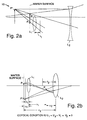
- Figs. 2a and 2b show paraxial solutions to the problem of inserting a magnifying system, comprising the moveable cofocal optical system 37, into an existing optical system without causing the final focal point (at the CCD array 35) to shift.
- Two lenses L 1 , L 2 are shown in Figs. 2a and 2b and correspond to the cofocal optical system 37 and the zoom lens 34, respectively in Fig. 1.
- the first lens L 1 provides a virtual erect image P' of the surface of the wafer 11 derived from an image P since the surface of the wafer 11 is located within the focal length of the first lens L 1 .
- This virtual image P' is magnified to produce image P'', but it is in the wrong plane and is moved back to the plane of the wafer 11 by being reimaged by the second (negative) lens L 2 to produce the image P'.
- Fig 2b shows a similar scheme using two positive lenses L 1 , L 2 to reposition an inverted image P' derived from an image P at the original object plane to produce the image P''.
- the magnifying system or moveable cofocal optical system 37 may need three positive lenses so that the pupils of the scattering screen 32 or the zoom lens 34 can be imaged onto one of the subsystem lens apertures.
Landscapes
- Physics & Mathematics (AREA)
- General Physics & Mathematics (AREA)
- Length Measuring Devices By Optical Means (AREA)
- Testing Or Measuring Of Semiconductors Or The Like (AREA)
Claims (8)
- Optisches System (10), umfassend:Abbildungseinrichtungen (34) niedriger Auflösung zum Abbilden eines Wafers bzw. einer Halbleiterscheibe (11) bei einer ersten vorbestimmten Auflösung, um ein Bild niedriger Auflösung des Wafers (11) zu erzeugen;Abbildungseinrichtungen (37) hoher Auflösung zum Abbilden eines Teilbereichs des Wafers (11) bei einer relativ hohen, vorbestimmten Auflösung, um ein Bild hoher Auflösung des Teilbereichs zu erzeugen, worin die Bilder niedriger und hoher Auflösung des Wafers in derselben Ebene fokussiert sind; undBilderzeugungseinrichtungen (35) zum Erzeugen eines Bildes des Wafers (11), welches aus den Bildern abgeleitet ist, welche von den Abbildungseinrichtungen (34, 37) niedriger und hoher Auflösung bereitgestellt sind;
dadurch gekennzeichnet, daß das optische System (10), welches zur Herstellung von Dickenmessungen eines Teilbereichs eines mit Mustern versehenen Wafers (11) dient, weiters umfaßt:Lichterzeugungseinrichtungen (12) zum Bereitstellen von Licht zur Beleuchtung des mit einem Muster versehenen Wafers (11); undVerarbeitungseinrichtungen (38) zum Bestimmen der Dicke von dünnen Filmen des Wafers entsprechend dem Teilbereich unter Verwendung von Daten, welche aus den Bildern hoher und niedriger Auflösung abgeleitet sind. - Optisches System (10) nach Anspruch 1, worin die Abbildungseinrichtungen (37) hoher Auflösung gekennzeichnet sind durch eine relativ kleine Abtastlinse (37) im Vergleich zum Wafer (11), welche adaptiert ist, um ein Bild auf die Bilderzeugungseinrichtungen (35) zu fokussieren.
- Optisches System (10) nach Anspruch 1, worin die Abbildungseinrichtungen (37) hoher Auflösung gekennzeichnet sind durch ein aufgelockertes Feld von Linsen (37), welches adaptiert ist, um ein Bild auf die Bilderzeugungseinrichtungen (35) zu fokussieren.
- Optisches System (10) nach Anspruch 2 oder Anspruch 3, worin die Bilderzeugungseinrichtungen (35) gekennzeichnet sind durch eine Kamera (35a) und eine Zoomlinse (34), welche adaptiert ist, um ein Bild auf die Kamera (35a) zu fokussieren.
- Optisches System (10) nach einem der vorhergehenden Ansprüche,worin die Lichterzeugungseinrichtungen (12) gekennzeichnet sind durch eine spektral gefilterte Lichtquelle (12) hoher Intensität;worin die Abbildungseinrichtungen (34) niedriger Auflösung gekennzeichnet sind durch:ein Faseroptikbündel (13), welches optisch mit der Lichtquelle (12) für ein Übertragen von dadurch bereitgestelltem Licht gekoppelt sind;eine Linsengruppe (15, 17), welche optisch mit dem Faseroptikbündel (13) zum Empfang des dadurch übertragenen Lichts gekoppelt ist;eine Kollimationslinse (31), welche optisch mit der Linsengruppe (15, 17) für ein Kollimieren des dadurch übertragenen Lichts gekoppelt ist;einen Diffusor (32), welcher optisch mit der Kollimationslinse (31) gekoppelt ist, um zu bewirken, daß Licht von dieser gestreut wird, um eine diffuse Lichtquelle (18) bereitzustellen;einen Strahlteiler (33), welcher optisch mit dem Diffusor (32) zum Reflektieren von Licht auf den gemusterten Wafer (11) gekoppelt ist;eine Zoomlinse (34) zum Abbilden von von dem Wafer (11) reflektiertem Licht mit einer ersten vorbestimmten Auflösung auf die Bilderzeugungseinrichtungen (35);worin die Bilderzeugungseinrichtungen (35) gekennzeichnet sind durch ein CCD-Feld (35); undworin die Abbildungseinrichtungen (37) hoher Auflösung gekennzeichnet sind durch ein bewegbares, konfokales, optisches System (37), welches zwischen dem Wafer (11) und der Zoomlinse (34) zum Abbilden eines kleinen Bereichs des Wafers (11) bei einer zweiten, vorbestimmten Auflösung angeordnet ist, welche größer ist als die Auflösung der Zoomlinse (34), um ein vergrößertes Bild in derselben Objektebene wie der Wafer (11) zu erzeugen;und worin das optische System weiters dadurch gekennzeichnet ist, daß der Prozessor (38) mit dem CCD-Feld bzw. Array (35) gekoppelt ist, welches eine Bibliothek bzw. Datenbank (39) umfaßt, welche Reflexionswerte beinhaltet, welche verschiedenen Werten von Filmdicken entsprechen, welche vorab bei unterschiedlichen Wellenlängen berechnet sind, und worin der Prozessor Einrichtungen zum Bestimmen der Reflexion des Wafers (11) unter Verwendung der Bilder hoher und niedriger Auflösung und Einrichtungen zum Vergleichen des berechneten, spektralen Reflexionsvermögens mit den vorberechneten Werten umfaßt, um die dementsprechende Dicke des Films des Wafers zu bestimmen.
- Optisches System (10) nach Anspruch 5, worin die spektral gefilterte Lichtquelle (12) hoher Intensität eine Halogenlampe umfaßt.
- Optisches System (10) nach Anspruch 5 oder Anspruch 6, worin die Linsengruppe (15, 17) eine Konkavlinse (15) und eine Konvexlinse (17) umfaßt.
- Optisches System (10) nach einem der Ansprüche 5 bis 7, worin die spektral gefilterte Lichtquelle (12) hoher Intensität einen Motorantrieb (21) umfaßt, welcher mit einem Filterrad (23) gekoppelt ist.
Applications Claiming Priority (2)
| Application Number | Priority Date | Filing Date | Title |
|---|---|---|---|
| US134729 | 1993-10-12 | ||
| US08/134,729 US5436725A (en) | 1993-10-12 | 1993-10-12 | Cofocal optical system for thickness measurements of patterned wafers |
Publications (3)
| Publication Number | Publication Date |
|---|---|
| EP0647828A2 EP0647828A2 (de) | 1995-04-12 |
| EP0647828A3 EP0647828A3 (de) | 1996-11-13 |
| EP0647828B1 true EP0647828B1 (de) | 2000-05-03 |
Family
ID=22464720
Family Applications (1)
| Application Number | Title | Priority Date | Filing Date |
|---|---|---|---|
| EP94307402A Expired - Lifetime EP0647828B1 (de) | 1993-10-12 | 1994-10-10 | Optisches Konfokalsystem für Dickenmessungen an einer Halbleiterscheibe mit einem Muster |
Country Status (6)
| Country | Link |
|---|---|
| US (1) | US5436725A (de) |
| EP (1) | EP0647828B1 (de) |
| JP (1) | JP2515090B2 (de) |
| DE (1) | DE69424246T2 (de) |
| IL (1) | IL111218A (de) |
| NO (1) | NO943839L (de) |
Families Citing this family (35)
| Publication number | Priority date | Publication date | Assignee | Title |
|---|---|---|---|---|
| US5555474A (en) * | 1994-12-21 | 1996-09-10 | Integrated Process Equipment Corp. | Automatic rejection of diffraction effects in thin film metrology |
| US5640242A (en) * | 1996-01-31 | 1997-06-17 | International Business Machines Corporation | Assembly and method for making in process thin film thickness measurments |
| WO2000055686A1 (en) * | 1997-05-21 | 2000-09-21 | Joseph Lyons | Passive shaped chuck for correcting field curvature |
| US6337698B1 (en) * | 1998-11-20 | 2002-01-08 | Microsoft Corporation | Pen-based interface for a notepad computer |
| US6690473B1 (en) * | 1999-02-01 | 2004-02-10 | Sensys Instruments Corporation | Integrated surface metrology |
| US6122064A (en) * | 1999-05-28 | 2000-09-19 | Philips Electronics North America Corporation | Method for measuring thickness of films |
| US9607301B2 (en) * | 2000-04-27 | 2017-03-28 | Merck Patent Gmbh | Photovoltaic sensor facilities in a home environment |
| KR20010100724A (ko) * | 2000-05-06 | 2001-11-14 | 임쌍근 | 마이크로 머신기술로 제작된 멀티미러 어레이의 평가계측장비 |
| US7095511B2 (en) * | 2000-07-06 | 2006-08-22 | Filmetrics, Inc. | Method and apparatus for high-speed thickness mapping of patterned thin films |
| US6940592B2 (en) * | 2001-10-09 | 2005-09-06 | Applied Materials, Inc. | Calibration as well as measurement on the same workpiece during fabrication |
| EP1446703A2 (de) * | 2001-11-07 | 2004-08-18 | Applied Materials, Inc. | Matrixbelichtungsgerät |
| US6946655B2 (en) | 2001-11-07 | 2005-09-20 | Applied Materials, Inc. | Spot grid array electron imaging system |
| US6639201B2 (en) * | 2001-11-07 | 2003-10-28 | Applied Materials, Inc. | Spot grid array imaging system |
| CN1602451A (zh) | 2001-11-07 | 2005-03-30 | 应用材料有限公司 | 无掩膜光子电子点格栅阵列光刻机 |
| WO2004084279A1 (en) * | 2003-03-14 | 2004-09-30 | Midwest Research Institute | Wafer characteristics via reflectometry |
| KR100546796B1 (ko) * | 2003-07-21 | 2006-01-25 | 동부아남반도체 주식회사 | 두께와 광학 이미지의 라이브러리를 이용한 절연막검사방법 |
| US7084966B2 (en) * | 2003-10-20 | 2006-08-01 | Infineon Technologies Ag | Optical measurement of device features using lenslet array illumination |
| WO2005083352A1 (en) * | 2004-02-11 | 2005-09-09 | Filmetrics, Inc. | Method and apparatus for high-speed thickness mapping of patterned thin films |
| US7910822B1 (en) * | 2005-10-17 | 2011-03-22 | Solaria Corporation | Fabrication process for photovoltaic cell |
| US8227688B1 (en) | 2005-10-17 | 2012-07-24 | Solaria Corporation | Method and resulting structure for assembling photovoltaic regions onto lead frame members for integration on concentrating elements for solar cells |
| US7444198B2 (en) | 2006-12-15 | 2008-10-28 | Applied Materials, Inc. | Determining physical property of substrate |
| US7840375B2 (en) * | 2007-04-02 | 2010-11-23 | Applied Materials, Inc. | Methods and apparatus for generating a library of spectra |
| US7910392B2 (en) | 2007-04-02 | 2011-03-22 | Solaria Corporation | Method and system for assembling a solar cell package |
| US20090056806A1 (en) * | 2007-09-05 | 2009-03-05 | Solaria Corporation | Solar cell structure including a plurality of concentrator elements with a notch design and predetermined radii and method |
| US8119902B2 (en) | 2007-05-21 | 2012-02-21 | Solaria Corporation | Concentrating module and method of manufacture for photovoltaic strips |
| US7910035B2 (en) | 2007-12-12 | 2011-03-22 | Solaria Corporation | Method and system for manufacturing integrated molded concentrator photovoltaic device |
| KR101151274B1 (ko) * | 2010-01-07 | 2012-06-14 | 주식회사 쓰리비 시스템 | 결점 검사장치 |
| CN101825760B (zh) * | 2010-03-24 | 2011-12-14 | 苏州大学 | 一种大口径球面主镜 |
| JP5365581B2 (ja) * | 2010-05-28 | 2013-12-11 | 信越半導体株式会社 | 薄膜付ウェーハの評価方法 |
| USD699176S1 (en) | 2011-06-02 | 2014-02-11 | Solaria Corporation | Fastener for solar modules |
| CN103673884B (zh) * | 2013-12-26 | 2016-09-14 | 北京信息科技大学 | 双三角光学测头的光路系统 |
| US9891048B2 (en) * | 2014-01-29 | 2018-02-13 | Advanced Semiconductor Engineering, Inc. | Measurement equipment |
| CN105937885B (zh) * | 2016-04-29 | 2018-08-14 | 浙江大学 | 一种自由曲面子孔径拼接干涉检测中被测面定位匹配方法 |
| DE102016115827A1 (de) * | 2016-08-25 | 2018-03-01 | Nanofocus Ag | Verfahren und Vorrichtung zur optischen Oberflächenmessung mit Hilfe eines chromatisch konfokalen Sensors |
| US20180172425A1 (en) * | 2016-12-21 | 2018-06-21 | The Penn State Research Foundation | High definition optical coherence tomography imaging for non-invasive examination of heritage works |
Family Cites Families (12)
| Publication number | Priority date | Publication date | Assignee | Title |
|---|---|---|---|---|
| GB2046432B (en) * | 1979-04-09 | 1983-05-11 | Infrared Eng Ltd | Apparatus for determining the thickness moisture content or other parameter of a film or coating |
| JPS57167651A (en) * | 1981-04-07 | 1982-10-15 | Mitsubishi Electric Corp | Inspecting device for surface of semiconductor wafer |
| US4845373A (en) * | 1984-02-22 | 1989-07-04 | Kla Instruments Corporation | Automatic alignment apparatus having low and high resolution optics for coarse and fine adjusting |
| JPS6157805U (de) * | 1984-09-20 | 1986-04-18 | ||
| US4659220A (en) * | 1984-10-22 | 1987-04-21 | International Business Machines Corporation | Optical inspection system for semiconductor wafers |
| JPS61155804A (ja) * | 1984-12-28 | 1986-07-15 | Toshiba Electron Syst Kk | 光学式水膜厚計 |
| US4651200A (en) * | 1985-02-04 | 1987-03-17 | National Biomedical Research Foundation | Split-image, multi-power microscopic image display system and method |
| JPH01110243A (ja) * | 1987-10-23 | 1989-04-26 | Hitachi Vlsi Eng Corp | 外観検査装置 |
| SU1755244A1 (ru) * | 1990-07-23 | 1992-08-15 | Ленинградский Институт Точной Механики И Оптики | Препаравальна лупа |
| CA2033130C (en) * | 1990-12-24 | 1996-12-31 | Brian William Petelka | Waterproof side rolling tarp system |
| US5291269A (en) * | 1991-12-06 | 1994-03-01 | Hughes Aircraft Company | Apparatus and method for performing thin film layer thickness metrology on a thin film layer having shape deformations and local slope variations |
| US5293214A (en) * | 1991-12-06 | 1994-03-08 | Hughes Aircraft Company | Apparatus and method for performing thin film layer thickness metrology by deforming a thin film layer into a reflective condenser |
-
1993
- 1993-10-12 US US08/134,729 patent/US5436725A/en not_active Expired - Lifetime
-
1994
- 1994-10-10 EP EP94307402A patent/EP0647828B1/de not_active Expired - Lifetime
- 1994-10-10 DE DE69424246T patent/DE69424246T2/de not_active Expired - Lifetime
- 1994-10-10 IL IL11121894A patent/IL111218A/en not_active IP Right Cessation
- 1994-10-11 NO NO943839A patent/NO943839L/no unknown
- 1994-10-12 JP JP6246337A patent/JP2515090B2/ja not_active Expired - Lifetime
Also Published As
| Publication number | Publication date |
|---|---|
| US5436725A (en) | 1995-07-25 |
| EP0647828A2 (de) | 1995-04-12 |
| NO943839D0 (no) | 1994-10-11 |
| EP0647828A3 (de) | 1996-11-13 |
| JP2515090B2 (ja) | 1996-07-10 |
| IL111218A (en) | 1996-11-14 |
| DE69424246D1 (de) | 2000-06-08 |
| JPH07181019A (ja) | 1995-07-18 |
| IL111218A0 (en) | 1994-12-29 |
| DE69424246T2 (de) | 2000-12-14 |
| NO943839L (no) | 1995-04-18 |
Similar Documents
| Publication | Publication Date | Title |
|---|---|---|
| EP0647828B1 (de) | Optisches Konfokalsystem für Dickenmessungen an einer Halbleiterscheibe mit einem Muster | |
| US6388808B1 (en) | Confocal microscopic equipment | |
| US6181427B1 (en) | Compact optical reflectometer system | |
| KR0165726B1 (ko) | 층 두께 결정 장치 및 방법 | |
| JP2001526383A (ja) | トロイダルミラー付きの反射分光光度装置 | |
| JP2648440B2 (ja) | 変形した形状及び部分的に変化した傾斜を有する薄膜層上の薄膜層の厚みを計測学的に処理するための装置及びその方法 | |
| US7547874B2 (en) | Single axis illumination for multi-axis imaging system | |
| US8437002B2 (en) | Imaging optical inspection device with a pinhole camera | |
| US7724358B2 (en) | Illuminator for darkfield inspection | |
| US20140268105A1 (en) | Optical defect inspection system | |
| WO1993016373A1 (en) | Apparatus for optical inspection of patterned substrates | |
| WO1993010425A1 (en) | Spectroscopic sampling accessory having dual measuring and viewing system | |
| US9239237B2 (en) | Optical alignment apparatus and methodology for a video based metrology tool | |
| FR2517837A1 (fr) | Dispositif optimisant le couplage de deux systemes optiques pour l'observation et l'analyse d'objets | |
| JP3388285B2 (ja) | 検査装置 | |
| US6271963B1 (en) | Microscope illuminator for cylindrical objects | |
| US5835265A (en) | Large numerical aperture imaging device | |
| JP3219462B2 (ja) | 薄膜測定器 | |
| RU69634U1 (ru) | Прибор для обнаружения и классификации дефектов оптических объектов (варианты) | |
| EP0845112B1 (de) | Reflektierende mikroskopvorrichtung | |
| US5872631A (en) | Optical two- and three-dimensional measuring of protrusions and convex surfaces | |
| JP2001336919A (ja) | リード付き集積回路の検査システム | |
| Fütterer et al. | Cobotic inspection of surface imperfections with collimated illumination | |
| JPS6110164Y2 (de) | ||
| Bietry et al. | Nomarski viewing system for an optical surface profiler |
Legal Events
| Date | Code | Title | Description |
|---|---|---|---|
| PUAI | Public reference made under article 153(3) epc to a published international application that has entered the european phase |
Free format text: ORIGINAL CODE: 0009012 |
|
| AK | Designated contracting states |
Kind code of ref document: A2 Designated state(s): CH DE FR GB LI NL SE |
|
| PUAL | Search report despatched |
Free format text: ORIGINAL CODE: 0009013 |
|
| AK | Designated contracting states |
Kind code of ref document: A3 Designated state(s): CH DE FR GB LI NL SE |
|
| 17P | Request for examination filed |
Effective date: 19970411 |
|
| RAP1 | Party data changed (applicant data changed or rights of an application transferred) |
Owner name: IPEC PRECISION, INC. |
|
| 17Q | First examination report despatched |
Effective date: 19980226 |
|
| GRAG | Despatch of communication of intention to grant |
Free format text: ORIGINAL CODE: EPIDOS AGRA |
|
| GRAG | Despatch of communication of intention to grant |
Free format text: ORIGINAL CODE: EPIDOS AGRA |
|
| GRAH | Despatch of communication of intention to grant a patent |
Free format text: ORIGINAL CODE: EPIDOS IGRA |
|
| GRAH | Despatch of communication of intention to grant a patent |
Free format text: ORIGINAL CODE: EPIDOS IGRA |
|
| GRAA | (expected) grant |
Free format text: ORIGINAL CODE: 0009210 |
|
| AK | Designated contracting states |
Kind code of ref document: B1 Designated state(s): CH DE FR GB LI NL SE |
|
| PG25 | Lapsed in a contracting state [announced via postgrant information from national office to epo] |
Ref country code: NL Free format text: LAPSE BECAUSE OF FAILURE TO SUBMIT A TRANSLATION OF THE DESCRIPTION OR TO PAY THE FEE WITHIN THE PRESCRIBED TIME-LIMIT Effective date: 20000503 Ref country code: LI Free format text: LAPSE BECAUSE OF FAILURE TO SUBMIT A TRANSLATION OF THE DESCRIPTION OR TO PAY THE FEE WITHIN THE PRESCRIBED TIME-LIMIT Effective date: 20000503 Ref country code: CH Free format text: LAPSE BECAUSE OF FAILURE TO SUBMIT A TRANSLATION OF THE DESCRIPTION OR TO PAY THE FEE WITHIN THE PRESCRIBED TIME-LIMIT Effective date: 20000503 |
|
| REG | Reference to a national code |
Ref country code: CH Ref legal event code: EP |
|
| REF | Corresponds to: |
Ref document number: 69424246 Country of ref document: DE Date of ref document: 20000608 |
|
| ET | Fr: translation filed | ||
| PG25 | Lapsed in a contracting state [announced via postgrant information from national office to epo] |
Ref country code: SE Free format text: LAPSE BECAUSE OF FAILURE TO SUBMIT A TRANSLATION OF THE DESCRIPTION OR TO PAY THE FEE WITHIN THE PRESCRIBED TIME-LIMIT Effective date: 20000803 |
|
| NLV1 | Nl: lapsed or annulled due to failure to fulfill the requirements of art. 29p and 29m of the patents act | ||
| REG | Reference to a national code |
Ref country code: CH Ref legal event code: PL |
|
| PLBE | No opposition filed within time limit |
Free format text: ORIGINAL CODE: 0009261 |
|
| STAA | Information on the status of an ep patent application or granted ep patent |
Free format text: STATUS: NO OPPOSITION FILED WITHIN TIME LIMIT |
|
| 26N | No opposition filed | ||
| REG | Reference to a national code |
Ref country code: GB Ref legal event code: IF02 |
|
| PGFP | Annual fee paid to national office [announced via postgrant information from national office to epo] |
Ref country code: GB Payment date: 20031001 Year of fee payment: 10 |
|
| PG25 | Lapsed in a contracting state [announced via postgrant information from national office to epo] |
Ref country code: GB Free format text: LAPSE BECAUSE OF NON-PAYMENT OF DUE FEES Effective date: 20041010 |
|
| GBPC | Gb: european patent ceased through non-payment of renewal fee |
Effective date: 20041010 |
|
| PGFP | Annual fee paid to national office [announced via postgrant information from national office to epo] |
Ref country code: DE Payment date: 20131029 Year of fee payment: 20 Ref country code: FR Payment date: 20131017 Year of fee payment: 20 |
|
| REG | Reference to a national code |
Ref country code: DE Ref legal event code: R071 Ref document number: 69424246 Country of ref document: DE |
|
| P01 | Opt-out of the competence of the unified patent court (upc) registered |
Effective date: 20230525 |