EP0641153A1 - Verfahren zur Herstellung von elektronischen Schaltungen unter der Oberfläche - Google Patents
Verfahren zur Herstellung von elektronischen Schaltungen unter der Oberfläche Download PDFInfo
- Publication number
- EP0641153A1 EP0641153A1 EP94306220A EP94306220A EP0641153A1 EP 0641153 A1 EP0641153 A1 EP 0641153A1 EP 94306220 A EP94306220 A EP 94306220A EP 94306220 A EP94306220 A EP 94306220A EP 0641153 A1 EP0641153 A1 EP 0641153A1
- Authority
- EP
- European Patent Office
- Prior art keywords
- channel
- layer
- substrate
- circuit
- curable
- Prior art date
- Legal status (The legal status is an assumption and is not a legal conclusion. Google has not performed a legal analysis and makes no representation as to the accuracy of the status listed.)
- Withdrawn
Links
- 238000004519 manufacturing process Methods 0.000 title claims abstract description 12
- 239000000463 material Substances 0.000 claims abstract description 56
- 239000000758 substrate Substances 0.000 claims abstract description 49
- 239000004020 conductor Substances 0.000 claims abstract description 39
- 238000000034 method Methods 0.000 claims description 59
- 238000012216 screening Methods 0.000 claims description 10
- 239000002904 solvent Substances 0.000 claims description 6
- 238000005406 washing Methods 0.000 claims description 5
- 239000002245 particle Substances 0.000 claims description 3
- 238000005507 spraying Methods 0.000 claims 1
- 239000003989 dielectric material Substances 0.000 abstract description 4
- 239000000945 filler Substances 0.000 abstract 1
- 239000002184 metal Substances 0.000 abstract 1
- 239000010410 layer Substances 0.000 description 29
- 229910000679 solder Inorganic materials 0.000 description 16
- 239000004568 cement Substances 0.000 description 12
- 230000008569 process Effects 0.000 description 10
- 239000000853 adhesive Substances 0.000 description 7
- 230000001070 adhesive effect Effects 0.000 description 7
- 239000000839 emulsion Substances 0.000 description 7
- 239000000976 ink Substances 0.000 description 5
- 229920002120 photoresistant polymer Polymers 0.000 description 5
- 230000008901 benefit Effects 0.000 description 4
- 229920000642 polymer Polymers 0.000 description 4
- 238000005476 soldering Methods 0.000 description 4
- RYGMFSIKBFXOCR-UHFFFAOYSA-N Copper Chemical compound [Cu] RYGMFSIKBFXOCR-UHFFFAOYSA-N 0.000 description 3
- 230000000903 blocking effect Effects 0.000 description 3
- 229920001940 conductive polymer Polymers 0.000 description 3
- 229910052802 copper Inorganic materials 0.000 description 3
- 239000010949 copper Substances 0.000 description 3
- 238000000151 deposition Methods 0.000 description 3
- 238000013461 design Methods 0.000 description 3
- LQBJWKCYZGMFEV-UHFFFAOYSA-N lead tin Chemical compound [Sn].[Pb] LQBJWKCYZGMFEV-UHFFFAOYSA-N 0.000 description 3
- 239000000203 mixture Substances 0.000 description 3
- 239000000126 substance Substances 0.000 description 3
- 238000012360 testing method Methods 0.000 description 3
- 239000004593 Epoxy Substances 0.000 description 2
- BQCADISMDOOEFD-UHFFFAOYSA-N Silver Chemical compound [Ag] BQCADISMDOOEFD-UHFFFAOYSA-N 0.000 description 2
- 238000004140 cleaning Methods 0.000 description 2
- 238000005530 etching Methods 0.000 description 2
- 238000007373 indentation Methods 0.000 description 2
- 239000007788 liquid Substances 0.000 description 2
- 230000008018 melting Effects 0.000 description 2
- 238000002844 melting Methods 0.000 description 2
- 238000005580 one pot reaction Methods 0.000 description 2
- 230000003287 optical effect Effects 0.000 description 2
- 239000011241 protective layer Substances 0.000 description 2
- 231100000331 toxic Toxicity 0.000 description 2
- 230000002588 toxic effect Effects 0.000 description 2
- 239000002699 waste material Substances 0.000 description 2
- NIXOWILDQLNWCW-UHFFFAOYSA-M Acrylate Chemical compound [O-]C(=O)C=C NIXOWILDQLNWCW-UHFFFAOYSA-M 0.000 description 1
- OKTJSMMVPCPJKN-UHFFFAOYSA-N Carbon Chemical compound [C] OKTJSMMVPCPJKN-UHFFFAOYSA-N 0.000 description 1
- 229920000106 Liquid crystal polymer Polymers 0.000 description 1
- 239000004977 Liquid-crystal polymers (LCPs) Substances 0.000 description 1
- 241000242532 Polycladida Species 0.000 description 1
- 241000220010 Rhode Species 0.000 description 1
- ATJFFYVFTNAWJD-UHFFFAOYSA-N Tin Chemical compound [Sn] ATJFFYVFTNAWJD-UHFFFAOYSA-N 0.000 description 1
- 230000009471 action Effects 0.000 description 1
- 239000006227 byproduct Substances 0.000 description 1
- 230000015556 catabolic process Effects 0.000 description 1
- 239000011248 coating agent Substances 0.000 description 1
- 238000000576 coating method Methods 0.000 description 1
- 238000011960 computer-aided design Methods 0.000 description 1
- 239000011231 conductive filler Substances 0.000 description 1
- 238000011109 contamination Methods 0.000 description 1
- 238000007796 conventional method Methods 0.000 description 1
- 238000005336 cracking Methods 0.000 description 1
- 230000008021 deposition Effects 0.000 description 1
- 230000008030 elimination Effects 0.000 description 1
- 238000003379 elimination reaction Methods 0.000 description 1
- 239000003344 environmental pollutant Substances 0.000 description 1
- 230000005496 eutectics Effects 0.000 description 1
- 238000005429 filling process Methods 0.000 description 1
- 229920005570 flexible polymer Polymers 0.000 description 1
- 230000004907 flux Effects 0.000 description 1
- 239000003365 glass fiber Substances 0.000 description 1
- 229910002804 graphite Inorganic materials 0.000 description 1
- 239000010439 graphite Substances 0.000 description 1
- 239000003673 groundwater Substances 0.000 description 1
- 238000003384 imaging method Methods 0.000 description 1
- 238000001746 injection moulding Methods 0.000 description 1
- 239000011344 liquid material Substances 0.000 description 1
- 150000002825 nitriles Chemical class 0.000 description 1
- 230000008520 organization Effects 0.000 description 1
- 238000004806 packaging method and process Methods 0.000 description 1
- 231100000719 pollutant Toxicity 0.000 description 1
- 229920000728 polyester Polymers 0.000 description 1
- 229920001601 polyetherimide Polymers 0.000 description 1
- 229940104181 polyflex Drugs 0.000 description 1
- 239000004814 polyurethane Substances 0.000 description 1
- 229920002635 polyurethane Polymers 0.000 description 1
- 238000012545 processing Methods 0.000 description 1
- 239000000047 product Substances 0.000 description 1
- 230000009467 reduction Effects 0.000 description 1
- 239000011347 resin Substances 0.000 description 1
- 229920005989 resin Polymers 0.000 description 1
- 239000002356 single layer Substances 0.000 description 1
- 239000000243 solution Substances 0.000 description 1
- XLYOFNOQVPJJNP-UHFFFAOYSA-N water Substances O XLYOFNOQVPJJNP-UHFFFAOYSA-N 0.000 description 1
Images


Classifications
-
- H—ELECTRICITY
- H01—ELECTRIC ELEMENTS
- H01L—SEMICONDUCTOR DEVICES NOT COVERED BY CLASS H10
- H01L24/00—Arrangements for connecting or disconnecting semiconductor or solid-state bodies; Methods or apparatus related thereto
- H01L24/80—Methods for connecting semiconductor or other solid state bodies using means for bonding being attached to, or being formed on, the surface to be connected
- H01L24/83—Methods for connecting semiconductor or other solid state bodies using means for bonding being attached to, or being formed on, the surface to be connected using a layer connector
-
- C—CHEMISTRY; METALLURGY
- C09—DYES; PAINTS; POLISHES; NATURAL RESINS; ADHESIVES; COMPOSITIONS NOT OTHERWISE PROVIDED FOR; APPLICATIONS OF MATERIALS NOT OTHERWISE PROVIDED FOR
- C09J—ADHESIVES; NON-MECHANICAL ASPECTS OF ADHESIVE PROCESSES IN GENERAL; ADHESIVE PROCESSES NOT PROVIDED FOR ELSEWHERE; USE OF MATERIALS AS ADHESIVES
- C09J163/00—Adhesives based on epoxy resins; Adhesives based on derivatives of epoxy resins
-
- H—ELECTRICITY
- H01—ELECTRIC ELEMENTS
- H01B—CABLES; CONDUCTORS; INSULATORS; SELECTION OF MATERIALS FOR THEIR CONDUCTIVE, INSULATING OR DIELECTRIC PROPERTIES
- H01B1/00—Conductors or conductive bodies characterised by the conductive materials; Selection of materials as conductors
- H01B1/20—Conductive material dispersed in non-conductive organic material
- H01B1/22—Conductive material dispersed in non-conductive organic material the conductive material comprising metals or alloys
-
- H—ELECTRICITY
- H01—ELECTRIC ELEMENTS
- H01L—SEMICONDUCTOR DEVICES NOT COVERED BY CLASS H10
- H01L21/00—Processes or apparatus adapted for the manufacture or treatment of semiconductor or solid state devices or of parts thereof
- H01L21/02—Manufacture or treatment of semiconductor devices or of parts thereof
- H01L21/04—Manufacture or treatment of semiconductor devices or of parts thereof the devices having potential barriers, e.g. a PN junction, depletion layer or carrier concentration layer
- H01L21/48—Manufacture or treatment of parts, e.g. containers, prior to assembly of the devices, using processes not provided for in a single one of the subgroups H01L21/06 - H01L21/326
- H01L21/4814—Conductive parts
- H01L21/4846—Leads on or in insulating or insulated substrates, e.g. metallisation
- H01L21/4867—Applying pastes or inks, e.g. screen printing
-
- H—ELECTRICITY
- H01—ELECTRIC ELEMENTS
- H01L—SEMICONDUCTOR DEVICES NOT COVERED BY CLASS H10
- H01L24/00—Arrangements for connecting or disconnecting semiconductor or solid-state bodies; Methods or apparatus related thereto
- H01L24/01—Means for bonding being attached to, or being formed on, the surface to be connected, e.g. chip-to-package, die-attach, "first-level" interconnects; Manufacturing methods related thereto
- H01L24/26—Layer connectors, e.g. plate connectors, solder or adhesive layers; Manufacturing methods related thereto
- H01L24/28—Structure, shape, material or disposition of the layer connectors prior to the connecting process
- H01L24/29—Structure, shape, material or disposition of the layer connectors prior to the connecting process of an individual layer connector
-
- H—ELECTRICITY
- H01—ELECTRIC ELEMENTS
- H01L—SEMICONDUCTOR DEVICES NOT COVERED BY CLASS H10
- H01L24/00—Arrangements for connecting or disconnecting semiconductor or solid-state bodies; Methods or apparatus related thereto
- H01L24/80—Methods for connecting semiconductor or other solid state bodies using means for bonding being attached to, or being formed on, the surface to be connected
- H01L24/81—Methods for connecting semiconductor or other solid state bodies using means for bonding being attached to, or being formed on, the surface to be connected using a bump connector
-
- H—ELECTRICITY
- H01—ELECTRIC ELEMENTS
- H01R—ELECTRICALLY-CONDUCTIVE CONNECTIONS; STRUCTURAL ASSOCIATIONS OF A PLURALITY OF MUTUALLY-INSULATED ELECTRICAL CONNECTING ELEMENTS; COUPLING DEVICES; CURRENT COLLECTORS
- H01R4/00—Electrically-conductive connections between two or more conductive members in direct contact, i.e. touching one another; Means for effecting or maintaining such contact; Electrically-conductive connections having two or more spaced connecting locations for conductors and using contact members penetrating insulation
- H01R4/04—Electrically-conductive connections between two or more conductive members in direct contact, i.e. touching one another; Means for effecting or maintaining such contact; Electrically-conductive connections having two or more spaced connecting locations for conductors and using contact members penetrating insulation using electrically conductive adhesives
-
- H—ELECTRICITY
- H05—ELECTRIC TECHNIQUES NOT OTHERWISE PROVIDED FOR
- H05K—PRINTED CIRCUITS; CASINGS OR CONSTRUCTIONAL DETAILS OF ELECTRIC APPARATUS; MANUFACTURE OF ASSEMBLAGES OF ELECTRICAL COMPONENTS
- H05K3/00—Apparatus or processes for manufacturing printed circuits
- H05K3/10—Apparatus or processes for manufacturing printed circuits in which conductive material is applied to the insulating support in such a manner as to form the desired conductive pattern
- H05K3/12—Apparatus or processes for manufacturing printed circuits in which conductive material is applied to the insulating support in such a manner as to form the desired conductive pattern using thick film techniques, e.g. printing techniques to apply the conductive material or similar techniques for applying conductive paste or ink patterns
- H05K3/1258—Apparatus or processes for manufacturing printed circuits in which conductive material is applied to the insulating support in such a manner as to form the desired conductive pattern using thick film techniques, e.g. printing techniques to apply the conductive material or similar techniques for applying conductive paste or ink patterns by using a substrate provided with a shape pattern, e.g. grooves, banks, resist pattern
-
- H—ELECTRICITY
- H05—ELECTRIC TECHNIQUES NOT OTHERWISE PROVIDED FOR
- H05K—PRINTED CIRCUITS; CASINGS OR CONSTRUCTIONAL DETAILS OF ELECTRIC APPARATUS; MANUFACTURE OF ASSEMBLAGES OF ELECTRICAL COMPONENTS
- H05K3/00—Apparatus or processes for manufacturing printed circuits
- H05K3/30—Assembling printed circuits with electric components, e.g. with resistor
- H05K3/32—Assembling printed circuits with electric components, e.g. with resistor electrically connecting electric components or wires to printed circuits
- H05K3/321—Assembling printed circuits with electric components, e.g. with resistor electrically connecting electric components or wires to printed circuits by conductive adhesives
-
- C—CHEMISTRY; METALLURGY
- C08—ORGANIC MACROMOLECULAR COMPOUNDS; THEIR PREPARATION OR CHEMICAL WORKING-UP; COMPOSITIONS BASED THEREON
- C08L—COMPOSITIONS OF MACROMOLECULAR COMPOUNDS
- C08L2666/00—Composition of polymers characterized by a further compound in the blend, being organic macromolecular compounds, natural resins, waxes or and bituminous materials, non-macromolecular organic substances, inorganic substances or characterized by their function in the composition
- C08L2666/54—Inorganic substances
-
- H—ELECTRICITY
- H01—ELECTRIC ELEMENTS
- H01L—SEMICONDUCTOR DEVICES NOT COVERED BY CLASS H10
- H01L2224/00—Indexing scheme for arrangements for connecting or disconnecting semiconductor or solid-state bodies and methods related thereto as covered by H01L24/00
- H01L2224/01—Means for bonding being attached to, or being formed on, the surface to be connected, e.g. chip-to-package, die-attach, "first-level" interconnects; Manufacturing methods related thereto
- H01L2224/10—Bump connectors; Manufacturing methods related thereto
- H01L2224/12—Structure, shape, material or disposition of the bump connectors prior to the connecting process
- H01L2224/13—Structure, shape, material or disposition of the bump connectors prior to the connecting process of an individual bump connector
- H01L2224/13001—Core members of the bump connector
- H01L2224/13099—Material
- H01L2224/131—Material with a principal constituent of the material being a metal or a metalloid, e.g. boron [B], silicon [Si], germanium [Ge], arsenic [As], antimony [Sb], tellurium [Te] and polonium [Po], and alloys thereof
- H01L2224/13101—Material with a principal constituent of the material being a metal or a metalloid, e.g. boron [B], silicon [Si], germanium [Ge], arsenic [As], antimony [Sb], tellurium [Te] and polonium [Po], and alloys thereof the principal constituent melting at a temperature of less than 400°C
- H01L2224/13111—Tin [Sn] as principal constituent
-
- H—ELECTRICITY
- H01—ELECTRIC ELEMENTS
- H01L—SEMICONDUCTOR DEVICES NOT COVERED BY CLASS H10
- H01L2224/00—Indexing scheme for arrangements for connecting or disconnecting semiconductor or solid-state bodies and methods related thereto as covered by H01L24/00
- H01L2224/01—Means for bonding being attached to, or being formed on, the surface to be connected, e.g. chip-to-package, die-attach, "first-level" interconnects; Manufacturing methods related thereto
- H01L2224/26—Layer connectors, e.g. plate connectors, solder or adhesive layers; Manufacturing methods related thereto
- H01L2224/28—Structure, shape, material or disposition of the layer connectors prior to the connecting process
- H01L2224/29—Structure, shape, material or disposition of the layer connectors prior to the connecting process of an individual layer connector
- H01L2224/29001—Core members of the layer connector
- H01L2224/29099—Material
- H01L2224/291—Material with a principal constituent of the material being a metal or a metalloid, e.g. boron [B], silicon [Si], germanium [Ge], arsenic [As], antimony [Sb], tellurium [Te] and polonium [Po], and alloys thereof
- H01L2224/29101—Material with a principal constituent of the material being a metal or a metalloid, e.g. boron [B], silicon [Si], germanium [Ge], arsenic [As], antimony [Sb], tellurium [Te] and polonium [Po], and alloys thereof the principal constituent melting at a temperature of less than 400°C
-
- H—ELECTRICITY
- H01—ELECTRIC ELEMENTS
- H01L—SEMICONDUCTOR DEVICES NOT COVERED BY CLASS H10
- H01L2224/00—Indexing scheme for arrangements for connecting or disconnecting semiconductor or solid-state bodies and methods related thereto as covered by H01L24/00
- H01L2224/01—Means for bonding being attached to, or being formed on, the surface to be connected, e.g. chip-to-package, die-attach, "first-level" interconnects; Manufacturing methods related thereto
- H01L2224/26—Layer connectors, e.g. plate connectors, solder or adhesive layers; Manufacturing methods related thereto
- H01L2224/28—Structure, shape, material or disposition of the layer connectors prior to the connecting process
- H01L2224/29—Structure, shape, material or disposition of the layer connectors prior to the connecting process of an individual layer connector
- H01L2224/29001—Core members of the layer connector
- H01L2224/29099—Material
- H01L2224/2919—Material with a principal constituent of the material being a polymer, e.g. polyester, phenolic based polymer, epoxy
-
- H—ELECTRICITY
- H01—ELECTRIC ELEMENTS
- H01L—SEMICONDUCTOR DEVICES NOT COVERED BY CLASS H10
- H01L2224/00—Indexing scheme for arrangements for connecting or disconnecting semiconductor or solid-state bodies and methods related thereto as covered by H01L24/00
- H01L2224/01—Means for bonding being attached to, or being formed on, the surface to be connected, e.g. chip-to-package, die-attach, "first-level" interconnects; Manufacturing methods related thereto
- H01L2224/26—Layer connectors, e.g. plate connectors, solder or adhesive layers; Manufacturing methods related thereto
- H01L2224/28—Structure, shape, material or disposition of the layer connectors prior to the connecting process
- H01L2224/29—Structure, shape, material or disposition of the layer connectors prior to the connecting process of an individual layer connector
- H01L2224/29001—Core members of the layer connector
- H01L2224/29099—Material
- H01L2224/29198—Material with a principal constituent of the material being a combination of two or more materials in the form of a matrix with a filler, i.e. being a hybrid material, e.g. segmented structures, foams
- H01L2224/29298—Fillers
- H01L2224/29399—Coating material
-
- H—ELECTRICITY
- H01—ELECTRIC ELEMENTS
- H01L—SEMICONDUCTOR DEVICES NOT COVERED BY CLASS H10
- H01L2224/00—Indexing scheme for arrangements for connecting or disconnecting semiconductor or solid-state bodies and methods related thereto as covered by H01L24/00
- H01L2224/80—Methods for connecting semiconductor or other solid state bodies using means for bonding being attached to, or being formed on, the surface to be connected
- H01L2224/81—Methods for connecting semiconductor or other solid state bodies using means for bonding being attached to, or being formed on, the surface to be connected using a bump connector
- H01L2224/818—Bonding techniques
- H01L2224/81801—Soldering or alloying
-
- H—ELECTRICITY
- H01—ELECTRIC ELEMENTS
- H01L—SEMICONDUCTOR DEVICES NOT COVERED BY CLASS H10
- H01L2224/00—Indexing scheme for arrangements for connecting or disconnecting semiconductor or solid-state bodies and methods related thereto as covered by H01L24/00
- H01L2224/80—Methods for connecting semiconductor or other solid state bodies using means for bonding being attached to, or being formed on, the surface to be connected
- H01L2224/83—Methods for connecting semiconductor or other solid state bodies using means for bonding being attached to, or being formed on, the surface to be connected using a layer connector
- H01L2224/8319—Arrangement of the layer connectors prior to mounting
-
- H—ELECTRICITY
- H01—ELECTRIC ELEMENTS
- H01L—SEMICONDUCTOR DEVICES NOT COVERED BY CLASS H10
- H01L2224/00—Indexing scheme for arrangements for connecting or disconnecting semiconductor or solid-state bodies and methods related thereto as covered by H01L24/00
- H01L2224/80—Methods for connecting semiconductor or other solid state bodies using means for bonding being attached to, or being formed on, the surface to be connected
- H01L2224/83—Methods for connecting semiconductor or other solid state bodies using means for bonding being attached to, or being formed on, the surface to be connected using a layer connector
- H01L2224/838—Bonding techniques
-
- H—ELECTRICITY
- H01—ELECTRIC ELEMENTS
- H01L—SEMICONDUCTOR DEVICES NOT COVERED BY CLASS H10
- H01L2924/00—Indexing scheme for arrangements or methods for connecting or disconnecting semiconductor or solid-state bodies as covered by H01L24/00
- H01L2924/01—Chemical elements
- H01L2924/01005—Boron [B]
-
- H—ELECTRICITY
- H01—ELECTRIC ELEMENTS
- H01L—SEMICONDUCTOR DEVICES NOT COVERED BY CLASS H10
- H01L2924/00—Indexing scheme for arrangements or methods for connecting or disconnecting semiconductor or solid-state bodies as covered by H01L24/00
- H01L2924/01—Chemical elements
- H01L2924/01006—Carbon [C]
-
- H—ELECTRICITY
- H01—ELECTRIC ELEMENTS
- H01L—SEMICONDUCTOR DEVICES NOT COVERED BY CLASS H10
- H01L2924/00—Indexing scheme for arrangements or methods for connecting or disconnecting semiconductor or solid-state bodies as covered by H01L24/00
- H01L2924/01—Chemical elements
- H01L2924/01023—Vanadium [V]
-
- H—ELECTRICITY
- H01—ELECTRIC ELEMENTS
- H01L—SEMICONDUCTOR DEVICES NOT COVERED BY CLASS H10
- H01L2924/00—Indexing scheme for arrangements or methods for connecting or disconnecting semiconductor or solid-state bodies as covered by H01L24/00
- H01L2924/01—Chemical elements
- H01L2924/01027—Cobalt [Co]
-
- H—ELECTRICITY
- H01—ELECTRIC ELEMENTS
- H01L—SEMICONDUCTOR DEVICES NOT COVERED BY CLASS H10
- H01L2924/00—Indexing scheme for arrangements or methods for connecting or disconnecting semiconductor or solid-state bodies as covered by H01L24/00
- H01L2924/01—Chemical elements
- H01L2924/01029—Copper [Cu]
-
- H—ELECTRICITY
- H01—ELECTRIC ELEMENTS
- H01L—SEMICONDUCTOR DEVICES NOT COVERED BY CLASS H10
- H01L2924/00—Indexing scheme for arrangements or methods for connecting or disconnecting semiconductor or solid-state bodies as covered by H01L24/00
- H01L2924/01—Chemical elements
- H01L2924/01033—Arsenic [As]
-
- H—ELECTRICITY
- H01—ELECTRIC ELEMENTS
- H01L—SEMICONDUCTOR DEVICES NOT COVERED BY CLASS H10
- H01L2924/00—Indexing scheme for arrangements or methods for connecting or disconnecting semiconductor or solid-state bodies as covered by H01L24/00
- H01L2924/01—Chemical elements
- H01L2924/01047—Silver [Ag]
-
- H—ELECTRICITY
- H01—ELECTRIC ELEMENTS
- H01L—SEMICONDUCTOR DEVICES NOT COVERED BY CLASS H10
- H01L2924/00—Indexing scheme for arrangements or methods for connecting or disconnecting semiconductor or solid-state bodies as covered by H01L24/00
- H01L2924/01—Chemical elements
- H01L2924/0105—Tin [Sn]
-
- H—ELECTRICITY
- H01—ELECTRIC ELEMENTS
- H01L—SEMICONDUCTOR DEVICES NOT COVERED BY CLASS H10
- H01L2924/00—Indexing scheme for arrangements or methods for connecting or disconnecting semiconductor or solid-state bodies as covered by H01L24/00
- H01L2924/01—Chemical elements
- H01L2924/01074—Tungsten [W]
-
- H—ELECTRICITY
- H01—ELECTRIC ELEMENTS
- H01L—SEMICONDUCTOR DEVICES NOT COVERED BY CLASS H10
- H01L2924/00—Indexing scheme for arrangements or methods for connecting or disconnecting semiconductor or solid-state bodies as covered by H01L24/00
- H01L2924/01—Chemical elements
- H01L2924/01082—Lead [Pb]
-
- H—ELECTRICITY
- H01—ELECTRIC ELEMENTS
- H01L—SEMICONDUCTOR DEVICES NOT COVERED BY CLASS H10
- H01L2924/00—Indexing scheme for arrangements or methods for connecting or disconnecting semiconductor or solid-state bodies as covered by H01L24/00
- H01L2924/01—Chemical elements
- H01L2924/01087—Francium [Fr]
-
- H—ELECTRICITY
- H01—ELECTRIC ELEMENTS
- H01L—SEMICONDUCTOR DEVICES NOT COVERED BY CLASS H10
- H01L2924/00—Indexing scheme for arrangements or methods for connecting or disconnecting semiconductor or solid-state bodies as covered by H01L24/00
- H01L2924/013—Alloys
- H01L2924/0132—Binary Alloys
- H01L2924/01322—Eutectic Alloys, i.e. obtained by a liquid transforming into two solid phases
-
- H—ELECTRICITY
- H01—ELECTRIC ELEMENTS
- H01L—SEMICONDUCTOR DEVICES NOT COVERED BY CLASS H10
- H01L2924/00—Indexing scheme for arrangements or methods for connecting or disconnecting semiconductor or solid-state bodies as covered by H01L24/00
- H01L2924/013—Alloys
- H01L2924/014—Solder alloys
-
- H—ELECTRICITY
- H01—ELECTRIC ELEMENTS
- H01L—SEMICONDUCTOR DEVICES NOT COVERED BY CLASS H10
- H01L2924/00—Indexing scheme for arrangements or methods for connecting or disconnecting semiconductor or solid-state bodies as covered by H01L24/00
- H01L2924/06—Polymers
- H01L2924/0665—Epoxy resin
-
- H—ELECTRICITY
- H01—ELECTRIC ELEMENTS
- H01L—SEMICONDUCTOR DEVICES NOT COVERED BY CLASS H10
- H01L2924/00—Indexing scheme for arrangements or methods for connecting or disconnecting semiconductor or solid-state bodies as covered by H01L24/00
- H01L2924/06—Polymers
- H01L2924/078—Adhesive characteristics other than chemical
- H01L2924/0781—Adhesive characteristics other than chemical being an ohmic electrical conductor
-
- H—ELECTRICITY
- H01—ELECTRIC ELEMENTS
- H01L—SEMICONDUCTOR DEVICES NOT COVERED BY CLASS H10
- H01L2924/00—Indexing scheme for arrangements or methods for connecting or disconnecting semiconductor or solid-state bodies as covered by H01L24/00
- H01L2924/30—Technical effects
- H01L2924/301—Electrical effects
- H01L2924/3025—Electromagnetic shielding
-
- H—ELECTRICITY
- H05—ELECTRIC TECHNIQUES NOT OTHERWISE PROVIDED FOR
- H05K—PRINTED CIRCUITS; CASINGS OR CONSTRUCTIONAL DETAILS OF ELECTRIC APPARATUS; MANUFACTURE OF ASSEMBLAGES OF ELECTRICAL COMPONENTS
- H05K1/00—Printed circuits
- H05K1/02—Details
- H05K1/09—Use of materials for the conductive, e.g. metallic pattern
- H05K1/092—Dispersed materials, e.g. conductive pastes or inks
- H05K1/095—Dispersed materials, e.g. conductive pastes or inks for polymer thick films, i.e. having a permanent organic polymeric binder
-
- H—ELECTRICITY
- H05—ELECTRIC TECHNIQUES NOT OTHERWISE PROVIDED FOR
- H05K—PRINTED CIRCUITS; CASINGS OR CONSTRUCTIONAL DETAILS OF ELECTRIC APPARATUS; MANUFACTURE OF ASSEMBLAGES OF ELECTRICAL COMPONENTS
- H05K1/00—Printed circuits
- H05K1/18—Printed circuits structurally associated with non-printed electric components
- H05K1/181—Printed circuits structurally associated with non-printed electric components associated with surface mounted components
-
- H—ELECTRICITY
- H05—ELECTRIC TECHNIQUES NOT OTHERWISE PROVIDED FOR
- H05K—PRINTED CIRCUITS; CASINGS OR CONSTRUCTIONAL DETAILS OF ELECTRIC APPARATUS; MANUFACTURE OF ASSEMBLAGES OF ELECTRICAL COMPONENTS
- H05K2201/00—Indexing scheme relating to printed circuits covered by H05K1/00
- H05K2201/01—Dielectrics
- H05K2201/0104—Properties and characteristics in general
- H05K2201/0125—Shrinkable, e.g. heat-shrinkable polymer
-
- H—ELECTRICITY
- H05—ELECTRIC TECHNIQUES NOT OTHERWISE PROVIDED FOR
- H05K—PRINTED CIRCUITS; CASINGS OR CONSTRUCTIONAL DETAILS OF ELECTRIC APPARATUS; MANUFACTURE OF ASSEMBLAGES OF ELECTRICAL COMPONENTS
- H05K2201/00—Indexing scheme relating to printed circuits covered by H05K1/00
- H05K2201/02—Fillers; Particles; Fibers; Reinforcement materials
- H05K2201/0203—Fillers and particles
- H05K2201/0206—Materials
- H05K2201/0218—Composite particles, i.e. first metal coated with second metal
-
- H—ELECTRICITY
- H05—ELECTRIC TECHNIQUES NOT OTHERWISE PROVIDED FOR
- H05K—PRINTED CIRCUITS; CASINGS OR CONSTRUCTIONAL DETAILS OF ELECTRIC APPARATUS; MANUFACTURE OF ASSEMBLAGES OF ELECTRICAL COMPONENTS
- H05K2201/00—Indexing scheme relating to printed circuits covered by H05K1/00
- H05K2201/02—Fillers; Particles; Fibers; Reinforcement materials
- H05K2201/0203—Fillers and particles
- H05K2201/0206—Materials
- H05K2201/023—Hard particles, i.e. particles in conductive adhesive at least partly penetrating an electrode
-
- H—ELECTRICITY
- H05—ELECTRIC TECHNIQUES NOT OTHERWISE PROVIDED FOR
- H05K—PRINTED CIRCUITS; CASINGS OR CONSTRUCTIONAL DETAILS OF ELECTRIC APPARATUS; MANUFACTURE OF ASSEMBLAGES OF ELECTRICAL COMPONENTS
- H05K2201/00—Indexing scheme relating to printed circuits covered by H05K1/00
- H05K2201/02—Fillers; Particles; Fibers; Reinforcement materials
- H05K2201/0203—Fillers and particles
- H05K2201/0242—Shape of an individual particle
- H05K2201/0245—Flakes, flat particles or lamellar particles
-
- H—ELECTRICITY
- H05—ELECTRIC TECHNIQUES NOT OTHERWISE PROVIDED FOR
- H05K—PRINTED CIRCUITS; CASINGS OR CONSTRUCTIONAL DETAILS OF ELECTRIC APPARATUS; MANUFACTURE OF ASSEMBLAGES OF ELECTRICAL COMPONENTS
- H05K2201/00—Indexing scheme relating to printed circuits covered by H05K1/00
- H05K2201/02—Fillers; Particles; Fibers; Reinforcement materials
- H05K2201/0203—Fillers and particles
- H05K2201/0263—Details about a collection of particles
- H05K2201/0272—Mixed conductive particles, i.e. using different conductive particles, e.g. differing in shape
-
- H—ELECTRICITY
- H05—ELECTRIC TECHNIQUES NOT OTHERWISE PROVIDED FOR
- H05K—PRINTED CIRCUITS; CASINGS OR CONSTRUCTIONAL DETAILS OF ELECTRIC APPARATUS; MANUFACTURE OF ASSEMBLAGES OF ELECTRICAL COMPONENTS
- H05K2201/00—Indexing scheme relating to printed circuits covered by H05K1/00
- H05K2201/09—Shape and layout
- H05K2201/09009—Substrate related
- H05K2201/09036—Recesses or grooves in insulating substrate
-
- H—ELECTRICITY
- H05—ELECTRIC TECHNIQUES NOT OTHERWISE PROVIDED FOR
- H05K—PRINTED CIRCUITS; CASINGS OR CONSTRUCTIONAL DETAILS OF ELECTRIC APPARATUS; MANUFACTURE OF ASSEMBLAGES OF ELECTRICAL COMPONENTS
- H05K2201/00—Indexing scheme relating to printed circuits covered by H05K1/00
- H05K2201/09—Shape and layout
- H05K2201/09209—Shape and layout details of conductors
- H05K2201/09372—Pads and lands
- H05K2201/09472—Recessed pad for surface mounting; Recessed electrode of component
-
- H—ELECTRICITY
- H05—ELECTRIC TECHNIQUES NOT OTHERWISE PROVIDED FOR
- H05K—PRINTED CIRCUITS; CASINGS OR CONSTRUCTIONAL DETAILS OF ELECTRIC APPARATUS; MANUFACTURE OF ASSEMBLAGES OF ELECTRICAL COMPONENTS
- H05K2203/00—Indexing scheme relating to apparatus or processes for manufacturing printed circuits covered by H05K3/00
- H05K2203/03—Metal processing
- H05K2203/0307—Providing micro- or nanometer scale roughness on a metal surface, e.g. by plating of nodules or dendrites
-
- H—ELECTRICITY
- H05—ELECTRIC TECHNIQUES NOT OTHERWISE PROVIDED FOR
- H05K—PRINTED CIRCUITS; CASINGS OR CONSTRUCTIONAL DETAILS OF ELECTRIC APPARATUS; MANUFACTURE OF ASSEMBLAGES OF ELECTRICAL COMPONENTS
- H05K2203/00—Indexing scheme relating to apparatus or processes for manufacturing printed circuits covered by H05K3/00
- H05K2203/05—Patterning and lithography; Masks; Details of resist
- H05K2203/0562—Details of resist
- H05K2203/0568—Resist used for applying paste, ink or powder
-
- H—ELECTRICITY
- H05—ELECTRIC TECHNIQUES NOT OTHERWISE PROVIDED FOR
- H05K—PRINTED CIRCUITS; CASINGS OR CONSTRUCTIONAL DETAILS OF ELECTRIC APPARATUS; MANUFACTURE OF ASSEMBLAGES OF ELECTRICAL COMPONENTS
- H05K2203/00—Indexing scheme relating to apparatus or processes for manufacturing printed circuits covered by H05K3/00
- H05K2203/11—Treatments characterised by their effect, e.g. heating, cooling, roughening
- H05K2203/1105—Heating or thermal processing not related to soldering, firing, curing or laminating, e.g. for shaping the substrate or during finish plating
-
- H—ELECTRICITY
- H05—ELECTRIC TECHNIQUES NOT OTHERWISE PROVIDED FOR
- H05K—PRINTED CIRCUITS; CASINGS OR CONSTRUCTIONAL DETAILS OF ELECTRIC APPARATUS; MANUFACTURE OF ASSEMBLAGES OF ELECTRICAL COMPONENTS
- H05K2203/00—Indexing scheme relating to apparatus or processes for manufacturing printed circuits covered by H05K3/00
- H05K2203/14—Related to the order of processing steps
- H05K2203/1453—Applying the circuit pattern before another process, e.g. before filling of vias with conductive paste, before making printed resistors
-
- H—ELECTRICITY
- H05—ELECTRIC TECHNIQUES NOT OTHERWISE PROVIDED FOR
- H05K—PRINTED CIRCUITS; CASINGS OR CONSTRUCTIONAL DETAILS OF ELECTRIC APPARATUS; MANUFACTURE OF ASSEMBLAGES OF ELECTRICAL COMPONENTS
- H05K3/00—Apparatus or processes for manufacturing printed circuits
- H05K3/0011—Working of insulating substrates or insulating layers
- H05K3/0017—Etching of the substrate by chemical or physical means
- H05K3/0023—Etching of the substrate by chemical or physical means by exposure and development of a photosensitive insulating layer
-
- H—ELECTRICITY
- H05—ELECTRIC TECHNIQUES NOT OTHERWISE PROVIDED FOR
- H05K—PRINTED CIRCUITS; CASINGS OR CONSTRUCTIONAL DETAILS OF ELECTRIC APPARATUS; MANUFACTURE OF ASSEMBLAGES OF ELECTRICAL COMPONENTS
- H05K3/00—Apparatus or processes for manufacturing printed circuits
- H05K3/10—Apparatus or processes for manufacturing printed circuits in which conductive material is applied to the insulating support in such a manner as to form the desired conductive pattern
- H05K3/107—Apparatus or processes for manufacturing printed circuits in which conductive material is applied to the insulating support in such a manner as to form the desired conductive pattern by filling grooves in the support with conductive material
-
- H—ELECTRICITY
- H05—ELECTRIC TECHNIQUES NOT OTHERWISE PROVIDED FOR
- H05K—PRINTED CIRCUITS; CASINGS OR CONSTRUCTIONAL DETAILS OF ELECTRIC APPARATUS; MANUFACTURE OF ASSEMBLAGES OF ELECTRICAL COMPONENTS
- H05K3/00—Apparatus or processes for manufacturing printed circuits
- H05K3/22—Secondary treatment of printed circuits
- H05K3/28—Applying non-metallic protective coatings
-
- Y—GENERAL TAGGING OF NEW TECHNOLOGICAL DEVELOPMENTS; GENERAL TAGGING OF CROSS-SECTIONAL TECHNOLOGIES SPANNING OVER SEVERAL SECTIONS OF THE IPC; TECHNICAL SUBJECTS COVERED BY FORMER USPC CROSS-REFERENCE ART COLLECTIONS [XRACs] AND DIGESTS
- Y10—TECHNICAL SUBJECTS COVERED BY FORMER USPC
- Y10T—TECHNICAL SUBJECTS COVERED BY FORMER US CLASSIFICATION
- Y10T29/00—Metal working
- Y10T29/49—Method of mechanical manufacture
- Y10T29/49002—Electrical device making
- Y10T29/49117—Conductor or circuit manufacturing
- Y10T29/49124—On flat or curved insulated base, e.g., printed circuit, etc.
- Y10T29/4913—Assembling to base an electrical component, e.g., capacitor, etc.
- Y10T29/49144—Assembling to base an electrical component, e.g., capacitor, etc. by metal fusion
-
- Y—GENERAL TAGGING OF NEW TECHNOLOGICAL DEVELOPMENTS; GENERAL TAGGING OF CROSS-SECTIONAL TECHNOLOGIES SPANNING OVER SEVERAL SECTIONS OF THE IPC; TECHNICAL SUBJECTS COVERED BY FORMER USPC CROSS-REFERENCE ART COLLECTIONS [XRACs] AND DIGESTS
- Y10—TECHNICAL SUBJECTS COVERED BY FORMER USPC
- Y10T—TECHNICAL SUBJECTS COVERED BY FORMER US CLASSIFICATION
- Y10T29/00—Metal working
- Y10T29/49—Method of mechanical manufacture
- Y10T29/49002—Electrical device making
- Y10T29/49117—Conductor or circuit manufacturing
- Y10T29/49124—On flat or curved insulated base, e.g., printed circuit, etc.
- Y10T29/49155—Manufacturing circuit on or in base
Definitions
- This invention relates to an improved method of making electronic circuits. More particularly, this invention relates to an improved method of making subsurface electronic circuits by filling channels in dielectric material with electrically conductive polymeric materials.
- a rigid dielectric substrate is first covered with copper or other electrically conductive material. Then, after temporarily protecting that portion of the conductive layer that will form the desired circuit trace, a substantial amount of this layer is chemically etched away. The protection is then removed, leaving copper traces in desired locations.
- One or more circuit components are attached to the circuit traces, usually by melting eutectic tin-lead solder.
- Planar subsurface electronic circuits made by filling channels in rigid dielectric substrates with electrically conductive materials are not extensively used.
- IBM Technical Disclosure Bulletin Vol. 27, No. 5, October, 1984, "Subsurface Circuitry On Polymeric Substrates", by E.W. Mace discloses a method of forming subsurface circuits in an injection-moulded substrate having angled wall channels.
- a compliant elastomeric blade or squeegee is used to fill the channels with a polymeric thick film conductive paste.
- the paste was drawn across the surface of the substrate using the squeegee to fill molded-in circuit lands.
- the substrate was then turned 90° and the filling process was repeated.
- the paste was dried and cured to its final state, following which excess cured paste was buffed away. Only then were circuit components attached to the cured conductive-paste-filled channels by various methods, including soldering.
- This method has several characteristics. First, it takes two passes to fill the dielectric with the conductive paste. Second, unnecessary waste is produced because the substrate's surface must be sanded or buffed after the channels have been filled and cured to remove excess paste. Yet a third characteristic is that circuit components are placed onto the filled channels after the paste is cured. Thus, an additional step of electrically connecting the components to the paste is needed. Typically, this is achieved by soldering, which contains lead and is harmful to the environment.
- U.S. Patent 4,645,733 to Sullivan teaches a process which involves steps of: 1) covering a printed wiring substrate with a layer of photopolymer paste, 2) photographically producing a wiring pattern in the photopolymer, paste layer, 3) washing out uncured photopolymer to leave indentations in the cured photopolymer, 4) using a squeegee to fill the indentations with a conductive material, such as a polymer ink, and 5) hardening the conductive material.
- a conductive material such as a polymer ink
- This invention provides an improved method of making subsurface electronic circuits. The method involves:
- the substrate may be planar and may be rigid.
- Figures 1a - 1f illustrate the general steps in a method according to the present invention.
- the process begins with a rigid board base 10 as shown in Fig. 1a.
- a rigid board base 10 as shown in Fig. 1a.
- Many different materials may be used depending on the ultimate application of the circuit. Selection factors include flammability rating and the expected environment in which the circuit will operate (e.g., whether in the engine compartment of a motor vehicle, in a consumer's home, etc.).
- the invention is versatile and can address a wide variety of needs. There are few known limits to the types of material which could potentially be useful. Key characteristics of the substrate are that it should be relatively flat, must withstand 130° C. processing temperatures and must be able to adhere a photo-imagable resist material.
- the substrate can be flexible, and it is expected that flexible circuits made in accordance with the invention will be capable of flexing around an 8'' (20.3 cm) mandril without cracking traces.
- Suitable flexible substrate materials are liquid crystal polymers, polyetherimides and polyester.
- rigid 0.059'' (1.4 mm) thick glass fiber reinforced epoxy (known as FR-4) made by Polyclad Laminates, Franklin, NH is suitable.
- a photopolymer resist material 12 is applied to the substrate as shown in Fig. b.
- material There are two general classes of material: 1) adhere to the substrate. A wide variety of these materials are generally available from the DuPont Company for use as solder-masks. Most appropriate ones will retain integrity when etched to have lines that are 0.3 (7.6 ⁇ m) to 0.65 mil (165 ⁇ m) wide and separated by spacing approximately equal to their width. Materials offering less resolution (e.g.12.5 mil (320 ⁇ m), 20 mil (510 ⁇ m), 30 mil (760 ⁇ m) and higher) will be useful for less demanding applications. As will become apparent from description of the process below, a material is said to retain integrity as long as channel walls do not collapse during other process steps, and thus will not to cause short circuits between adjacent channels.
- Specialty techniques can also be used to apply the mask material, such as screen equipment which applies and simultaneously cures thin layers (20-30 ⁇ m) of liquid material. Key considerations are the resolution requirements of the final circuit, availability of material and cost. Unless applications demand otherwise, commercially available, dry-film solder mask material made from a photosensitive acrylate with good dielectric properties and capable of resolving 2 mil (51 ⁇ m) lines and spacing is suitable.
- the photoresist material is developed (e.g. exposed and cured) using procedures applicable to the selected material.
- a dry-film solder mask material an artwork film bearing an image of a desired circuit pattern is laid over the photoresist and exposed to ultraviolet (UV) light.
- UV light causes the photoresist to harden.
- Photoresist material shielded from the UV light by patterns imaged onto the art-work film (the desired circuit pattern) remains relatively soft.
- the shielded material removed by a high pressure wash using procedures suggested by the manufacture of the photoresist. What remains are channels 14 in the hardened photopolymer as shown in Fig. 1c.
- a conductive material 16 is applied to fill the channels in a manner that avoids remnants of conductive materials outside the channels.
- This deposition step is shown generally in Fig. 1d).
- One deposition method uses a doctor blade 18 to press material through a wire mesh screen (not shown in Fig. 1d but shown in greater detail in Fig. 4) that has been coated with a blocking material. The screen allows the conductive material to be deposited in a pattern that matches the channel pattern. This aspect will be discussed in more detail below. An alternate method will be discussed with reference to Figure 7.
- a number of suitable conductive materials are disclosed in U.S. patents 5,180,523 and 5,183,593, in copending U.S.
- the substrate is populated with circuit components 20 before the conductive material is permanently set, as illustrated in Fig. 1e.
- Electronic contacts 22 of the circuit components 20 are placed in contact with the uncured conductive adhesive 24.
- the conductive adhesive 24 is cured, which sets the conductive material in the channels 26 and makes physical and electrical connection to the leads 22 of the circuit components 20 as shown in Fig. 1f.
- the method is quite suitable to automatic component placement by machine. Curing temperatures of conductive adhesives will typically be less than 180° C, more often less than 160° C, and preferably less than 140° C--well below the temperatures usually used for melting traditional lead-tin solder.
- the components are covered with a protective layer.
- a protective layer may be an adhesive that distributes strain away from the contact/channel juncture.
- this method provides significant reduction in manufacturing cost by combining steps for curing the circuit and attaching the components. It will also be appreciated that this method reduces toxic by-products common to etching copper-clad substrates and traditional flux/solder processes. It will also be appreciated that, when using a flexible substrate, flexible polymer dielectric material, and flexible adhesive cement, the resulting circuit will be flexible.
- Figures 2a - 2d illustrate generally a circuit assembly made in accordance with the method of the present invention.
- Figure 2a shows a generalized circuit 30 having conductive traces 32 formed in the manner described above.
- Electronic components 36 of varying packaging designs may be applied.
- Figures 2b, 2c and 2d illustrate details of connections for varying types of packages including flip chips 38, surface mount devices (SMD) 40 and traditional feed-thru devices 42.
- SMD surface mount devices
- electrically conductive adhesive 44 in the channels binds to electrical connection points 46 on the respective packages, forming physical and electrical connections.
- Figures 3a - 3b illustrate details of steps for forming channels using a photo-imagable material.
- a vacuum table 50 holds a three-layer assembly in a fixed position.
- the three layer assembly includes a substrate 10 to which is attached a dry film photopolymer sheet 12 covered by a photo-tool 52 bearing an image of a circuit pattern to be formed.
- the photo-tool is made using circuit artwork production methods, usually CAD-based (computer aided design) that are well known in the electronics industry.
- CAD-based computer aided design
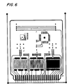
- An example circuit is shown in Figure 6.
- the photopolymer sheet is attached to the substrate using one of many well known techniques developed in other contexts of solder masks.
- the photopolymer is exposed to ultra violet energy 54, with dark traces imaged on the photo-tool serving to block the ultra violet energy in areas where channels will be formed.
- the photo-tool is removed and the pattern is developed, also using techniques developed for solder masks.
- the photo-tool 52 has been removed to expose the photopolymer to a high pressure chemical wash.
- the wash removes unexposed, soft photopolymer and leaves channels 58 in a pattern that corresponds to the circuit pattern imaged on the photo-tool. Details of exposure and washing will depend on the photo-imagable material selected and proceeds in accordance with the manufacturer's instructions.
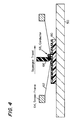
- Figure 4 illustrates details of steps for filling channels in a manner that avoids remnants of conductive materials outside the channels.
- the channel-bearing substrate 60 is held by the vacuum table 50 and positioned in a screening apparatus.
- the screen 62 is a wire mesh with wire diameter of .0007'' to .0009'' (18-23 ⁇ m) held in a frame 64. Larger wire sizes can be used as desired channel resolution becomes larger.
- the .0007'' (18 ⁇ m) and .0009'' (23 ⁇ m) sizes are appropriate for channel widths of 6.5 mil (165 ⁇ m).
- the screen 62 bears an image that matches the circuit formed on the substrate. That is, the screen has been coated with a blocking material except in a patten matching the channel pattern. Methods for making screens are known in the art, and any established practice capable of producing images with desired line resolution are suitable.
- a squeegee 66 spreads conductive cement 68 across the screen 64, driving cement through the screen into the channel.
- the screen has been coated with a blocking material and then imaged to leave openings that allow conductive cement to pass through in a pattern that corresponds to the channels.
- the action of the squeegee and the screen allow the channels to be fully filled without deposited cement between the channels.
- FIG. 4 depicts the screen as held slightly above the level of the channels.
- pressure applied by the squeegee presses the screen down to the channel level.
- tension in the screen lifts the screen back off the channel level, leaving no significant amounts of material outside the channels.
- This method of screening is known in other contexts for printing, and it is within the skill of the art to adjust screen tension and the distance between the screen level and the channel level for the particular screen press used.
- Circuit traces in a typical circuit layout tend to run along orthogonal directions, e.g., top-to-bottom or left-to-right.
- screens have wire which run in orthogonal directions. It is helpful to rotate the screen at an angle relative to the directions of the circuit to improve the application of the pattern.
- the screen will typically be rotated 0° - 450, more often 15° - 30°, and preferably 20° - 25° (e.g., 22.5 °).
- One method for aligning the screen to the channels uses registration marks on the photo-tool (used for creating the channels), registration marks on the screen, and an optical method for aligning the marks.
- substrates with channels are prepared using a pattern with a registration mark.
- a wire screen bearing a pattern identical to the channel and with an identically placed registration mark is loaded into a printing press and conductive cement is printed onto a blank substrate.
- a video camera mounted to the screen press images the location of the printed registration marks.
- the video system has a cross-hair or other adjustable indicator showing the location of the registration mark in the image. Then, the blank substrate is removed and replaced with a substrate having channels and bearing registration marks identical to the ones printed on the blank. The position of channelized substrate is channelized substrate are aligned with the cross-hair or other indicator showing the location of the registration mark of the blank.
- the vacuum table may be moved under electronic control until the images of the registration marks align. After the channelized substrate is aligned, the press is operated again to print through the screen and into the channels.
- Figures 5a - 5c illustrate details of a squeegee used to spread conductive material across a screen and into channels.
- Figure 5a is an end view showing the squeegee frame 70, a diamond-shaped polyurethane blade 72 and alignment screws, while Figures 5b and 5c are side and top views respectively.
- the alignment screws 74 allow height adjustment for leveling along the length of the blade 72.
- a simple squeegee design is preferred in order to simplify cleaning and avoid contamination (residue carried from one run to the next).
- circuits Four exemplary circuits are described which were formed using the screening procedure discussed above. All used a circuit design as shown in Figure 6. Different regions were designed to test different aspects of the process. Each example used a 24'' by 24'' (61 x 61 cm) wire screen and 8'' (20 cm. squeegee. All used FR-4 substrate with photopolymer film. The photo-tool was supplied to a commercial PC board manufacturer, Precision Coating Services, Massachusetts, who returned a channelized substrate using standard solder-mask techniques.
- Channelized substrates were then screen printed, each using different materials.
- the screens were aligned manually using the video imaging method described above.
- Channels were formed to a channel depth of about (48 ⁇ m) (48 ⁇ m) thickness of the photopolymer film).
- Fill level indicates the depth of the fill material. Depths are measured from the top of the channels, so that a positive value indicates that fill material rose above the channel, while a negative value indicates that material did not reach the top of the channel.
- conductive inks of Tables I and II which have higher contents of conductive particles than the conductive cement of Tables III and IV, have lower resistivity.
- conductive cements which having more adhesive, have higher resistivity. It is contemplated that the choice of material will depend on the ultimate circuit application. Those applications having greater demands on physical adhesion may prefer to use conductive cement, while circuits having greater demands on low resistivity may prefer to use conductive ink.
- a fifth example is described in which channels were filled using the screening method described above, but with variations in the dielectric material and the conductive composition used to fill the channels.
- the dielectric (mask material) used to make the channels was DuPont VALU (TM) solder mask (8400 Series/t-1197 Liquid) applied, imaged and developed in accordance with the manufacturer's method.
- the channel pattern was a set of parallel, interdigitated channels, each channel 5 mils (130 ⁇ m) thick, each channel separated by 5 mils (130 ⁇ m) mask. Channel depth was about 1.3 mil (33 ⁇ m).
- the conductive material used to fill the channels was mixture of 325 parts DuPont 5007 with 300 parts Acheson Colloids Co. SS-24747 (a graphite in Resin Solution not specifically formulated for conductivity). Although channels were initially fully filled, fill level after curing was about -0.87 mil (22 ⁇ m) (roughly 1/3 of the channel remained filled). Channels exhibited resistivity of about 70 ohms/inch (27.5 ohms/cm). The dielectric not breakdown when subjected to 2,000 volts between adjacent channels.
- hybrid method may be used in which substantial lengths of the channels are filled with conductive ink using a first screen and then remaining areas (e.g., bonding areas for electrical components) are filled with conductive cement using a second screen. Electrical components can then be placed, and both conductive materials cured together. Alternately, the ink may be cured before applying the cement. Even so, electrical components may be placed before curing the cement.
- a sixth example is described in which conductive materials is deposited without a screen, which is illustrated in Figure 7.
- a substrate 100 illustrated in Fig. 7a is similar to substrates used in Examples I-V.
- Two layers of mask material are applied to the substrate as illustrated in Fig. 7b.
- the first layer 102 is a liquid photo-imagable solder mask material, Enthone Enplate (TM) DSR 3241. It is drawn across the substrate and dried.
- the second layer 104 is a different photopolymer emulsion, such as Murakami One Pot Sol-C.
- a variety of emulsions may be used as long as the second (top) emulsion may be removed without also removing the first (lower) emulsion.
- the two emulsion layers are photo-imaged and developed in much the same manner as with a single emulsion in order to form channels 106 as illustrated in Fig. 7c.
- the emulsions may be exposed using UV light, and the uncured material washed away to leave channels 106. If necessary, two separate wash steps may be used, one to wash uncured material from each of the two layers 102, 104.
- a curable conductive material 112 (such as one of the Poly-Solder (TM) compositions used in Examples III) or IV) is then applied directly (without screening) to the two-layer assembly as illustrated in Fig. 7d.
- the curable conductive material may be drawn by hand across the assembly using an elastomeric squeegee 108, or by using a screening press without a screen. It can be expected that some uncured conductive material 110 will remain outside the channels.
- a pressure nozzle 114 dispensing a solvent 116 that reclaims the cured second (top) layer as illustrated in Fig. 7e.
- a suitable reclaiming solvent is ICC 833 stencil remover made by Intercontinental Chemical Corporation.
- the second layer 104 dissolves and washes away with the reclaiming solvent, it carries away any residual conductive material 110 that was deposited outside the channels.
- the reclaiming step selectively removes residual conductive material 110 which was mixed with the soluble second layer 104.
- the curable conductive material 112 is then applied to the curable conductive material 112 as shown in Fig. 7f. After placing components, the curable conductive material 112 is cured using ultra violet light 120 as illustrated in Fig. 7g.
- a further advantage of the present invention is the elimination of soldering heat. Many electronic components are susceptible to damage from the relatively high temperatures needed to melt solder. Although the present process uses heat to cure the conductive polymer, the temperatures are much lower--as low as 130° C for polymer cure, compared to over 180° C for lead-tin solder.
- multi-layer circuits can also be formed using these techniques.
- the process proceeds as described above until the step of placing components. Rather than placing components, polymer in the channels is cured. Then a new layer of photo-polymer is applied and new channels formed. After curing and cleaning the second photopolymer layer, channels in the second layer are filled with conductive material. Regions of overlap between this second layer and the (already cured) first layer act as connections (vias), because the bottom of a channel of the second layer is exposed to the top of a channel of the first layer. After applying conductive polymer to the second layer, components are placed and the second layer is cured. By extension, third and higher layers can be applied.
Landscapes
- Engineering & Computer Science (AREA)
- Microelectronics & Electronic Packaging (AREA)
- Computer Hardware Design (AREA)
- Power Engineering (AREA)
- Manufacturing & Machinery (AREA)
- Physics & Mathematics (AREA)
- Chemical & Material Sciences (AREA)
- Organic Chemistry (AREA)
- Dispersion Chemistry (AREA)
- Spectroscopy & Molecular Physics (AREA)
- Ceramic Engineering (AREA)
- Condensed Matter Physics & Semiconductors (AREA)
- General Physics & Mathematics (AREA)
- Manufacturing Of Printed Wiring (AREA)
Applications Claiming Priority (2)
| Application Number | Priority Date | Filing Date | Title |
|---|---|---|---|
| US08/112,225 US5531020A (en) | 1989-11-14 | 1993-08-27 | Method of making subsurface electronic circuits |
| US112225 | 1993-08-27 |
Publications (1)
| Publication Number | Publication Date |
|---|---|
| EP0641153A1 true EP0641153A1 (de) | 1995-03-01 |
Family
ID=22342742
Family Applications (1)
| Application Number | Title | Priority Date | Filing Date |
|---|---|---|---|
| EP94306220A Withdrawn EP0641153A1 (de) | 1993-08-27 | 1994-08-23 | Verfahren zur Herstellung von elektronischen Schaltungen unter der Oberfläche |
Country Status (2)
| Country | Link |
|---|---|
| US (1) | US5531020A (de) |
| EP (1) | EP0641153A1 (de) |
Cited By (1)
| Publication number | Priority date | Publication date | Assignee | Title |
|---|---|---|---|---|
| FR2837345A1 (fr) * | 2002-03-15 | 2003-09-19 | Novatec | Procede de remplissage de zones situees en creux sur un substrat |
Families Citing this family (63)
| Publication number | Priority date | Publication date | Assignee | Title |
|---|---|---|---|---|
| JP3587884B2 (ja) * | 1994-07-21 | 2004-11-10 | 富士通株式会社 | 多層回路基板の製造方法 |
| US5822856A (en) * | 1996-06-28 | 1998-10-20 | International Business Machines Corporation | Manufacturing circuit board assemblies having filled vias |
| US6125531A (en) * | 1999-03-01 | 2000-10-03 | International Business Machines Corporation | Method of making a printed circuit board having filled holes and a fill member for use therewith including reinforcement means |
| FR2793990B1 (fr) | 1999-05-19 | 2001-07-27 | Sagem | Boitier electronique sur plaque et procede de fabrication d'un tel boitier |
| US6734369B1 (en) * | 2000-08-31 | 2004-05-11 | International Business Machines Corporation | Surface laminar circuit board having pad disposed within a through hole |
| TW595283B (en) * | 2001-04-25 | 2004-06-21 | Benq Corp | Flexible circuit board and its manufacturing method |
| US7334326B1 (en) | 2001-06-19 | 2008-02-26 | Amkor Technology, Inc. | Method for making an integrated circuit substrate having embedded passive components |
| US6930256B1 (en) | 2002-05-01 | 2005-08-16 | Amkor Technology, Inc. | Integrated circuit substrate having laser-embedded conductive patterns and method therefor |
| US7399661B2 (en) * | 2002-05-01 | 2008-07-15 | Amkor Technology, Inc. | Method for making an integrated circuit substrate having embedded back-side access conductors and vias |
| US7670962B2 (en) | 2002-05-01 | 2010-03-02 | Amkor Technology, Inc. | Substrate having stiffener fabrication method |
| US6930257B1 (en) | 2002-05-01 | 2005-08-16 | Amkor Technology, Inc. | Integrated circuit substrate having laminated laser-embedded circuit layers |
| US9691635B1 (en) | 2002-05-01 | 2017-06-27 | Amkor Technology, Inc. | Buildup dielectric layer having metallization pattern semiconductor package fabrication method |
| US7633765B1 (en) | 2004-03-23 | 2009-12-15 | Amkor Technology, Inc. | Semiconductor package including a top-surface metal layer for implementing circuit features |
| US7548430B1 (en) | 2002-05-01 | 2009-06-16 | Amkor Technology, Inc. | Buildup dielectric and metallization process and semiconductor package |
| US20080043447A1 (en) * | 2002-05-01 | 2008-02-21 | Amkor Technology, Inc. | Semiconductor package having laser-embedded terminals |
| US11081370B2 (en) | 2004-03-23 | 2021-08-03 | Amkor Technology Singapore Holding Pte. Ltd. | Methods of manufacturing an encapsulated semiconductor device |
| US10811277B2 (en) | 2004-03-23 | 2020-10-20 | Amkor Technology, Inc. | Encapsulated semiconductor package |
| US7145238B1 (en) | 2004-05-05 | 2006-12-05 | Amkor Technology, Inc. | Semiconductor package and substrate having multi-level vias |
| KR100581221B1 (ko) * | 2004-06-30 | 2006-05-22 | 삼성전자주식회사 | 테이프 배선 기판 제조 방법 |
| CN100531514C (zh) * | 2004-07-12 | 2009-08-19 | 鸿富锦精密工业(深圳)有限公司 | 防止短路的印刷电路板结构 |
| US7703201B2 (en) * | 2004-10-25 | 2010-04-27 | International Business Machines Corporation | Method of embedding tamper proof layers and discrete components into printed circuit board stack-up |
| US8826531B1 (en) | 2005-04-05 | 2014-09-09 | Amkor Technology, Inc. | Method for making an integrated circuit substrate having laminated laser-embedded circuit layers |
| WO2006124400A2 (en) | 2005-05-13 | 2006-11-23 | University Of Pittsburgh - Of The Commonwealth System Of Higher Education | Method of making an electronic device using an electrically conductive polymer, and associated products |
| US20070012773A1 (en) * | 2005-06-07 | 2007-01-18 | University Of Pittsburgh - Of The Commonwealth System Of Higher Education | Method of making an electronic device using an electrically conductive polymer, and associated products |
| US7589398B1 (en) | 2006-10-04 | 2009-09-15 | Amkor Technology, Inc. | Embedded metal features structure |
| US7550857B1 (en) | 2006-11-16 | 2009-06-23 | Amkor Technology, Inc. | Stacked redistribution layer (RDL) die assembly package |
| US7750250B1 (en) | 2006-12-22 | 2010-07-06 | Amkor Technology, Inc. | Blind via capture pad structure |
| US20080156849A1 (en) * | 2007-01-03 | 2008-07-03 | International Business Machines Corporation | Mold shave apparatus and injection molded soldering process |
| US7752752B1 (en) | 2007-01-09 | 2010-07-13 | Amkor Technology, Inc. | Method of fabricating an embedded circuit pattern |
| US8323771B1 (en) | 2007-08-15 | 2012-12-04 | Amkor Technology, Inc. | Straight conductor blind via capture pad structure and fabrication method |
| JP5049744B2 (ja) * | 2007-11-05 | 2012-10-17 | 株式会社日立製作所 | 配線基板の製造方法およびその配線基板 |
| US8872329B1 (en) | 2009-01-09 | 2014-10-28 | Amkor Technology, Inc. | Extended landing pad substrate package structure and method |
| US7960827B1 (en) | 2009-04-09 | 2011-06-14 | Amkor Technology, Inc. | Thermal via heat spreader package and method |
| US8623753B1 (en) | 2009-05-28 | 2014-01-07 | Amkor Technology, Inc. | Stackable protruding via package and method |
| US8222538B1 (en) | 2009-06-12 | 2012-07-17 | Amkor Technology, Inc. | Stackable via package and method |
| US8471154B1 (en) | 2009-08-06 | 2013-06-25 | Amkor Technology, Inc. | Stackable variable height via package and method |
| US8796561B1 (en) | 2009-10-05 | 2014-08-05 | Amkor Technology, Inc. | Fan out build up substrate stackable package and method |
| US8937381B1 (en) | 2009-12-03 | 2015-01-20 | Amkor Technology, Inc. | Thin stackable package and method |
| US9691734B1 (en) | 2009-12-07 | 2017-06-27 | Amkor Technology, Inc. | Method of forming a plurality of electronic component packages |
| US8536462B1 (en) | 2010-01-22 | 2013-09-17 | Amkor Technology, Inc. | Flex circuit package and method |
| US8300423B1 (en) | 2010-05-25 | 2012-10-30 | Amkor Technology, Inc. | Stackable treated via package and method |
| US8294276B1 (en) | 2010-05-27 | 2012-10-23 | Amkor Technology, Inc. | Semiconductor device and fabricating method thereof |
| US8338229B1 (en) | 2010-07-30 | 2012-12-25 | Amkor Technology, Inc. | Stackable plasma cleaned via package and method |
| US8717775B1 (en) | 2010-08-02 | 2014-05-06 | Amkor Technology, Inc. | Fingerprint sensor package and method |
| US8337657B1 (en) | 2010-10-27 | 2012-12-25 | Amkor Technology, Inc. | Mechanical tape separation package and method |
| US8482134B1 (en) | 2010-11-01 | 2013-07-09 | Amkor Technology, Inc. | Stackable package and method |
| US9748154B1 (en) | 2010-11-04 | 2017-08-29 | Amkor Technology, Inc. | Wafer level fan out semiconductor device and manufacturing method thereof |
| US8525318B1 (en) | 2010-11-10 | 2013-09-03 | Amkor Technology, Inc. | Semiconductor device and fabricating method thereof |
| US8557629B1 (en) | 2010-12-03 | 2013-10-15 | Amkor Technology, Inc. | Semiconductor device having overlapped via apertures |
| US8535961B1 (en) | 2010-12-09 | 2013-09-17 | Amkor Technology, Inc. | Light emitting diode (LED) package and method |
| US9721872B1 (en) | 2011-02-18 | 2017-08-01 | Amkor Technology, Inc. | Methods and structures for increasing the allowable die size in TMV packages |
| US9013011B1 (en) | 2011-03-11 | 2015-04-21 | Amkor Technology, Inc. | Stacked and staggered die MEMS package and method |
| KR101140113B1 (ko) | 2011-04-26 | 2012-04-30 | 앰코 테크놀로지 코리아 주식회사 | 반도체 디바이스 |
| US8653674B1 (en) | 2011-09-15 | 2014-02-18 | Amkor Technology, Inc. | Electronic component package fabrication method and structure |
| US8633598B1 (en) | 2011-09-20 | 2014-01-21 | Amkor Technology, Inc. | Underfill contacting stacking balls package fabrication method and structure |
| US9029962B1 (en) | 2011-10-12 | 2015-05-12 | Amkor Technology, Inc. | Molded cavity substrate MEMS package fabrication method and structure |
| KR101366461B1 (ko) | 2012-11-20 | 2014-02-26 | 앰코 테크놀로지 코리아 주식회사 | 반도체 디바이스 및 그 제조 방법 |
| US9799592B2 (en) | 2013-11-19 | 2017-10-24 | Amkor Technology, Inc. | Semicondutor device with through-silicon via-less deep wells |
| KR101488590B1 (ko) | 2013-03-29 | 2015-01-30 | 앰코 테크놀로지 코리아 주식회사 | 반도체 디바이스 및 그 제조 방법 |
| KR101607981B1 (ko) | 2013-11-04 | 2016-03-31 | 앰코 테크놀로지 코리아 주식회사 | 반도체 패키지용 인터포저 및 이의 제조 방법, 제조된 인터포저를 이용한 반도체 패키지 |
| US9578771B2 (en) | 2014-03-18 | 2017-02-21 | Labinal, Llc | Backplane module and method of manufacturing same |
| US9960328B2 (en) | 2016-09-06 | 2018-05-01 | Amkor Technology, Inc. | Semiconductor device and manufacturing method thereof |
| WO2018145106A1 (en) * | 2017-02-06 | 2018-08-09 | Carnegie Mellon University | A flexible circuit and a method of manufacture |
Citations (6)
| Publication number | Priority date | Publication date | Assignee | Title |
|---|---|---|---|---|
| DE2231614A1 (de) * | 1972-06-28 | 1974-01-10 | Ulrich Dr Wegner | Verfahren zur herstellung gedruckter schaltungen unter verwendung eines photopolymers sowie einer leitfaehigen viskosen dispersion oder paste als stromleiter und vorrichtung zur durchfuehrung des verfahrens |
| GB1457805A (en) * | 1974-03-01 | 1976-12-08 | Mullard Ltd | Electric circuit modules |
| EP0195611A2 (de) * | 1985-03-16 | 1986-09-24 | Marconi Electronic Devices Limited | Gedruckte elektrische Schaltung und Verfahren zum Verbinden von Bauelementen mit dieser Schaltung |
| EP0250006A1 (de) * | 1986-06-13 | 1987-12-23 | Tektronix, Inc. | Gedruckte Schaltung mit Polymerplatte, Methode und Gerät |
| JPH02158191A (ja) * | 1988-12-12 | 1990-06-18 | Furukawa Electric Co Ltd:The | 部品実装回路基板の製造方法 |
| EP0542149A2 (de) * | 1991-11-11 | 1993-05-19 | Siemens Aktiengesellschaft | Verfahren zur Herstellung von Lotflächen auf einer Leiterplatte und Lotpastenfolie zur Durchführung des Verfahrens |
Family Cites Families (18)
| Publication number | Priority date | Publication date | Assignee | Title |
|---|---|---|---|---|
| BE568197A (de) * | 1957-06-12 | |||
| DE3014041C2 (de) * | 1980-04-11 | 1982-04-08 | Braun Ag, 6000 Frankfurt | Verfahren zur Aufbringung von elektrisch leitenden Bahnen auf einen Träger aus Isolierstoff |
| US4775611A (en) * | 1983-11-10 | 1988-10-04 | Sullivan Donald F | Additive printed circuit boards with flat surface and indented primary wiring conductors |
| US4756929A (en) * | 1983-11-10 | 1988-07-12 | Sullivan Donald F | High density printing wiring |
| US4645733A (en) * | 1983-11-10 | 1987-02-24 | Sullivan Donald F | High resolution printed circuits formed in photopolymer pattern indentations overlaying printed wiring board substrates |
| US4528259A (en) * | 1983-11-10 | 1985-07-09 | Sullivan Donald F | Printed wiring boards with solder mask over bare copper wires having large area thickened circuit pad connections |
| US4581098A (en) * | 1984-10-19 | 1986-04-08 | International Business Machines Corporation | MLC green sheet process |
| FR2599893B1 (fr) * | 1986-05-23 | 1996-08-02 | Ricoh Kk | Procede de montage d'un module electronique sur un substrat et carte a circuit integre |
| US4912020A (en) * | 1986-10-21 | 1990-03-27 | Westinghouse Electric Corp. | Printed circuit boards and method for manufacturing printed circuit boards |
| JPH03501822A (ja) * | 1987-10-10 | 1991-04-25 | ツインマー,ヨハネス | 塗着装置 |
| JPH0682926B2 (ja) * | 1988-04-22 | 1994-10-19 | 日本電気株式会社 | 多層配線基板の製造方法 |
| US5024372A (en) * | 1989-01-03 | 1991-06-18 | Motorola, Inc. | Method of making high density solder bumps and a substrate socket for high density solder bumps |
| US4985293A (en) * | 1989-08-14 | 1991-01-15 | Eastman Kodak Company | Polymer blend for molded circuit boards and other selectively conductive molded devices |
| US4982892A (en) * | 1989-11-09 | 1991-01-08 | International Business Machines Corporation | Solder interconnects for selective line coupling |
| US5183593A (en) * | 1989-11-14 | 1993-02-02 | Poly-Flex Circuits, Inc. | Electrically conductive cement |
| US5180523A (en) * | 1989-11-14 | 1993-01-19 | Poly-Flex Circuits, Inc. | Electrically conductive cement containing agglomerate, flake and powder metal fillers |
| US5034091A (en) * | 1990-04-27 | 1991-07-23 | Hughes Aircraft Company | Method of forming an electrical via structure |
| US5044306A (en) * | 1990-06-11 | 1991-09-03 | Gunter Erdmann | Solder applying mechanism |
-
1993
- 1993-08-27 US US08/112,225 patent/US5531020A/en not_active Expired - Lifetime
-
1994
- 1994-08-23 EP EP94306220A patent/EP0641153A1/de not_active Withdrawn
Patent Citations (6)
| Publication number | Priority date | Publication date | Assignee | Title |
|---|---|---|---|---|
| DE2231614A1 (de) * | 1972-06-28 | 1974-01-10 | Ulrich Dr Wegner | Verfahren zur herstellung gedruckter schaltungen unter verwendung eines photopolymers sowie einer leitfaehigen viskosen dispersion oder paste als stromleiter und vorrichtung zur durchfuehrung des verfahrens |
| GB1457805A (en) * | 1974-03-01 | 1976-12-08 | Mullard Ltd | Electric circuit modules |
| EP0195611A2 (de) * | 1985-03-16 | 1986-09-24 | Marconi Electronic Devices Limited | Gedruckte elektrische Schaltung und Verfahren zum Verbinden von Bauelementen mit dieser Schaltung |
| EP0250006A1 (de) * | 1986-06-13 | 1987-12-23 | Tektronix, Inc. | Gedruckte Schaltung mit Polymerplatte, Methode und Gerät |
| JPH02158191A (ja) * | 1988-12-12 | 1990-06-18 | Furukawa Electric Co Ltd:The | 部品実装回路基板の製造方法 |
| EP0542149A2 (de) * | 1991-11-11 | 1993-05-19 | Siemens Aktiengesellschaft | Verfahren zur Herstellung von Lotflächen auf einer Leiterplatte und Lotpastenfolie zur Durchführung des Verfahrens |
Non-Patent Citations (1)
| Title |
|---|
| PATENT ABSTRACTS OF JAPAN vol. 14, no. 413 (E - 0974) 6 September 1990 (1990-09-06) * |
Cited By (1)
| Publication number | Priority date | Publication date | Assignee | Title |
|---|---|---|---|---|
| FR2837345A1 (fr) * | 2002-03-15 | 2003-09-19 | Novatec | Procede de remplissage de zones situees en creux sur un substrat |
Also Published As
| Publication number | Publication date |
|---|---|
| US5531020A (en) | 1996-07-02 |
Similar Documents
| Publication | Publication Date | Title |
|---|---|---|
| US5531020A (en) | Method of making subsurface electronic circuits | |
| US7589010B2 (en) | Semiconductor devices with permanent polymer stencil and method for manufacturing the same | |
| KR100694251B1 (ko) | 반도체 디바이스 및 그 제조방법 | |
| KR100295732B1 (ko) | 인쇄배선기판홀충진방법 | |
| KR940007800B1 (ko) | 인쇄 배선 기판용 레지스트 패터닝방법 | |
| US4260675A (en) | Photoprinting plate and method of preparing printed circuit board solder masks therewith | |
| US6013417A (en) | Process for fabricating circuitry on substrates having plated through-holes | |
| US6838372B2 (en) | Via interconnect forming process and electronic component product thereof | |
| WO2001001739A1 (en) | Solder paste stenciling apparatus and method of use for rework | |
| US6641865B2 (en) | Method for selectively applying solder mask | |
| US6808643B2 (en) | Hybrid interconnect substrate and method of manufacture thereof | |
| JP2021172046A (ja) | スクリーンマスク、スクリーンマスクの製造方法及び印刷物の製造方法 | |
| EP0242020A2 (de) | Elektrische Schaltkreise | |
| JPH0766555A (ja) | 積層セラミック電子部品の製造方法 | |
| JP2748621B2 (ja) | 印刷配線板の製造方法 | |
| Liu et al. | Ultra-fine photoresist image formation for next generation high-density PWB substrate | |
| CA2652107C (en) | Solder void reduction on circuit boards | |
| JP2003092068A (ja) | プラズマディスプレイの背面板とその製造方法 | |
| KR0155887B1 (ko) | 인쇄회로기판의 이종부품실장을 위한 스크린 인쇄방법 및 그 장치 | |
| KR20230160023A (ko) | 실크스크린막이 코팅되어 방수성능이 향상된 pcb | |
| JPS6348890A (ja) | プリント配線板の製造装置 | |
| JP2997389B2 (ja) | スクリ−ン印刷方法及びスクリーン印刷機 | |
| JPH0422688A (ja) | 凹版及びその製造方法 | |
| JP2009111127A (ja) | 導電性パターンの形成方法 | |
| KR20060061073A (ko) | 솔더레지스트의 도포 방법 |
Legal Events
| Date | Code | Title | Description |
|---|---|---|---|
| PUAI | Public reference made under article 153(3) epc to a published international application that has entered the european phase |
Free format text: ORIGINAL CODE: 0009012 |
|
| AK | Designated contracting states |
Kind code of ref document: A1 Designated state(s): AT BE CH DE DK ES FR GB IE IT LI NL PT SE |
|
| RAX | Requested extension states of the european patent have changed |
Free format text: SI PAYMENT 941017 |
|
| STAA | Information on the status of an ep patent application or granted ep patent |
Free format text: STATUS: THE APPLICATION IS DEEMED TO BE WITHDRAWN |
|
| 18D | Application deemed to be withdrawn |
Effective date: 19950902 |