EP0640975B1 - Speicher, in dem eine Verbesserung durchgeführt wird, insbesondere die Vorladung von Ausgangsleseleitungen - Google Patents
Speicher, in dem eine Verbesserung durchgeführt wird, insbesondere die Vorladung von Ausgangsleseleitungen Download PDFInfo
- Publication number
- EP0640975B1 EP0640975B1 EP94113327A EP94113327A EP0640975B1 EP 0640975 B1 EP0640975 B1 EP 0640975B1 EP 94113327 A EP94113327 A EP 94113327A EP 94113327 A EP94113327 A EP 94113327A EP 0640975 B1 EP0640975 B1 EP 0640975B1
- Authority
- EP
- European Patent Office
- Prior art keywords
- signal
- read bus
- pairs
- read
- processing means
- Prior art date
- Legal status (The legal status is an assumption and is not a legal conclusion. Google has not performed a legal analysis and makes no representation as to the accuracy of the status listed.)
- Expired - Lifetime
Links
- 239000004065 semiconductor Substances 0.000 claims description 40
- 230000004044 response Effects 0.000 claims description 12
- 238000007599 discharging Methods 0.000 claims description 9
- 238000000034 method Methods 0.000 claims description 6
- 230000003213 activating effect Effects 0.000 claims description 5
- 238000010586 diagram Methods 0.000 description 6
- 230000001360 synchronised effect Effects 0.000 description 6
- 230000004913 activation Effects 0.000 description 4
- 239000000872 buffer Substances 0.000 description 3
- 230000001419 dependent effect Effects 0.000 description 3
- 101100489119 Saccharomyces cerevisiae (strain ATCC 204508 / S288c) YSW1 gene Proteins 0.000 description 2
- 238000011161 development Methods 0.000 description 2
- 230000018109 developmental process Effects 0.000 description 2
Images


Classifications
-
- G—PHYSICS
- G11—INFORMATION STORAGE
- G11C—STATIC STORES
- G11C11/00—Digital stores characterised by the use of particular electric or magnetic storage elements; Storage elements therefor
- G11C11/21—Digital stores characterised by the use of particular electric or magnetic storage elements; Storage elements therefor using electric elements
- G11C11/34—Digital stores characterised by the use of particular electric or magnetic storage elements; Storage elements therefor using electric elements using semiconductor devices
- G11C11/40—Digital stores characterised by the use of particular electric or magnetic storage elements; Storage elements therefor using electric elements using semiconductor devices using transistors
- G11C11/401—Digital stores characterised by the use of particular electric or magnetic storage elements; Storage elements therefor using electric elements using semiconductor devices using transistors forming cells needing refreshing or charge regeneration, i.e. dynamic cells
- G11C11/4063—Auxiliary circuits, e.g. for addressing, decoding, driving, writing, sensing or timing
- G11C11/407—Auxiliary circuits, e.g. for addressing, decoding, driving, writing, sensing or timing for memory cells of the field-effect type
-
- G—PHYSICS
- G11—INFORMATION STORAGE
- G11C—STATIC STORES
- G11C7/00—Arrangements for writing information into, or reading information out from, a digital store
- G11C7/10—Input/output [I/O] data interface arrangements, e.g. I/O data control circuits, I/O data buffers
- G11C7/1048—Data bus control circuits, e.g. precharging, presetting, equalising
Definitions
- This invention relates to a semiconductor memory device such as a synchronous dynamic random access memory (DRAM) and, in particular, to control a state of data readout routes through which data are read out from memory cells.
- DRAM synchronous dynamic random access memory
- a conventional synchronous DRAM comprises a period determining arrangement, a plurality of memory cells, a plurality of word lines, a plurality of bit line pairs, a first processing arrangement, a plurality of read bus pairs, and a second processing arrangement.
- the period determining arrangement is for determining a burst period.
- the word lines are connected to the memory cells.
- the bit line pairs are connected to the memory cells.
- Each of the bit line pairs comprises two bit lines having a bit line potential difference therebetween.
- the first processing arrangement is connected to the bit line pairs and is for processing the bit line potential difference into a first difference signal.
- the read bus pairs are connected to the first processing arrangement and supplied with the first difference signal.
- Each of the read bus pairs comprises two read buses having a read bus potential difference therebetween.
- the second processing arrangement is connected to the read bus pairs and is for processing the read bus potential difference into a second difference signal.
- the conventional synchronous DRAM further comprises a precharge circuit for carrying out a precharge operation to precharge each of the read bus pairs in response to necessity in the manner known in the art.
- a precharge circuit for carrying out a precharge operation to precharge each of the read bus pairs in response to necessity in the manner known in the art.
- each of the read bus pairs is electrically charged, amplified, and discharged in every one cycle having a cycle time. This results in a large consumption of charging/discharging current of each of the read bus pairs.
- the charging/discharging current generates a noise on a power supply line and on a ground line in the manner known in the art.
- JP-A-02294991 Another prior art example is disclosed in JP-A-02294991.
- selected ones of data readout routes are continuously and electrically charged for a predetermined time period.
- the burst mode is described in EP-A-0 468 480.
- DE-A-4211843 discloses a semiconductor memory device having all features of the preamble of claim 1 and claim 6 and consequently without the possibility of burst access. Therefore, for reading several successive memory cells the column addresses have to be generated externally and provided via a column address input.
- US-A- 5 291 450 discloses to switch off the precharging unit during read out.
- the conventional semiconductor memory device is a synchronous DRAM.
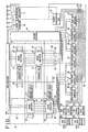
- the conventional semiconductor memory device comprises a command decoder 11, a pulse generating circuit 12, a burst counter 13, a column decoder 14, and a row decoder 15.
- the command decoder 11 is supplied with an external clock through a clock input terminal CLK, with a row address strobe signal through a row address input terminal RAS, with a column address strobe signal through a column address input terminal CAS, with a write signal through a write input terminal WE, and with an external address signal through an external signal input terminal All.
- the command decoder 11 produces an enabling signal and an activation signal.
- the pulse generating circuit 12 is connected to the clock input terminal CLK and the command decoder 11. Supplied with the external clock and the enabling signal, the pulse generating circuit 12 generates a first and a second pulse signal which will later become clear.
- the burst counter 13 is connected to an additional signal input terminal Ai and the command decoder 11. Supplied with the enabling signal and with a plurality of additional external address signals through the additional signal input terminal Ai, the burst counter 13 produces an internal address signal.
- the column decoder 14 is connected to the burst counter 13.
- the column decoder 14 produces a plurality of column selection,signals and a first and a second column address signal.
- the column selection signals will later be presented by symbols YAW1, YAW2, ...
- the row decoder 15 is connected to the command decoder 11 and the additional signal input terminal Ai.
- the row decoder 15 produces a plurality of plate selection signals and a plurality of word signals. Each of the plate selection signals has a first plate selection signal and a second plate selection signal modified from the first plate selection signal.
- the conventional semiconductor memory device further comprises a semiconductor array 16 connected to the column and the row decoders 14 and 15.
- the semiconductor array 16 comprises a large number of memory cells (only a few ones of which are depicted) 17, a plurality of word lines (only one of which is depicted) 18, and a plurality of bit line pairs (only a few ones of which are depicted) 19.
- the word lines 18 are connected to the row decoder 15 and supplied with the word signals.
- the bit line pairs 19 comprises two bit lines and are supplied with bit signals in the manner known in the art. It is assumed that the bit lines produce a potential difference therebetween which will later become clear. The potential difference will be referred to as a bit line potential difference.
- Each of the memory cells 17 is connected to each of the word lines 18 and to each of the bit line pairs 19 and is for memorizing a datum in accordance with one of the bit signals and with one of the word signals in the manner known in the art.
- the semiconductor array 16 further comprises a large number of sense amplifiers (only a few ones of which are depicted) 21 each of which is of a shared type known in the art.
- the sense amplifiers 21 are separated into a plurality of sense amplifier groups 22 each of which are directly connected to the row decoder 15. In each of the sense amplifier groups 22, the sense amplifiers 21 are serially connected to one another. In accordance with the bit line potential difference, each of the sense amplifier groups 22 produces, as a first difference signal, a first and a second read bus signal known in the art.
- the first and the second read bus signals are supplied to first and second read bus pairs 23 and 24, respectively, which are selected as selected ones from a large number of read bus pairs by the row decoder 15.
- each of the sense amplifier groups 22 supplies the first and the second plate selection signals to an array OR gate 25.
- Each of the sense amplifier groups 22 is referred to as a first processing arrangement.
- Each of the first and the second read bus pairs 23 and 24 comprises two read buses.
- the read buses of the first read bus pair 23 produce a potential difference therebetween which will be called hereunder a first read bus potential difference.
- the read buses of the second read bus pair 24 produce a potential difference therebetween which will be called hereunder a second read bus potential difference.
- the conventional semiconductor memory device further comprises a precharge control circuit 26, a first main data amplifier 27, a second main data amplifier 28, a first supplementary data amplifier 31, a second supplementary data amplifier 32.
- the precharge control circuit 26 is connected to the pulse generating circuit 12, the column decoder 14, and the array OR gate 25. In the manner which will later be described in detail, the precharge control circuit 26 produces a data amplifier enabling and a read bus precharging signal in accordance with the first and the second pulse signals, the first and the second column address signals, and a gate output signal which is supplied from the OR gate 25.
- the first main data amplifier 27 is connected to the first read bus pair 23 and the precharge control circuit 26 and is for amplifying the data amplifier enabling and the read bus precharging signals with reference to the first read bus potential difference into a first main amplified signal and a first main modified signal modified from the first main amplified signal.
- the first main amplified and the first main modified signals are supplied to the first supplementary data amplifier 31 through a first read write bus pair 33.
- the first supplementary data amplifier 31 amplifies the first main amplified and the first main modified signals to produce a first read out data signal as a second difference signal.
- the second main data amplifier 28 is connected to the second read bus pair 24 and the precharge control circuit 26 and is amplifying the data amplifier enabling and the read bus precharging signals with reference to the second read bus potential difference into a second main amplified signal and a second main modified signal modified from the second main amplified signal.
- the second main amplified and the second main modified signals are supplied to the second supplementary data amplifier 32 through a second read write bus pair 34.
- the second supplementary data amplifier 32 amplifies the second main amplified and the second main modified signals to produce a second read out data signal as the second difference signal.
- Each of the first and the second main data amplifiers 27 and 28 is referred to as a second processing arrangement.
- the conventional semiconductor memory device further comprises first and second data output buffers 35 and 36.
- the first data output buffer 35 is connected to the first supplementary data amplifier 31 and is for driving a first data output pad DQ1 in response to the first read out data signal.
- the second data output buffer 36 is connected to the second supplementary data amplifier 32 and is for driving a second data output pad DQ2 in response to the first read out data signal.
- the precharge control circuit 26 comprises an inverter 41, a NAND gate 42, a first NOR gate 43, and a second NOR gate 44.
- the inverter 41 is connected to the pulse generating circuit 12 and is for producing an inverted pulse signal in response to absence of the second pulse signal.
- the NAND gate 42 is connected to the array NOR gate 25 and the column decoder 14 and is for producing a local gate signal in accordance to absence of both of the gate output and the first column address signals.
- the first NOR gate 43 is connected to the inverter 41, the NAND gate 42, the first primary data amplifier 27, and the second primary data amplifier 28, and is for producing the read bus precharging signal in accordance with absence of at least one of the inverted pulse and the local gate signals.
- the second NOR gate 44 is connected to the NAND gate 42, the pulse generating circuit 12, the first primary data amplifier 27, and the second primary data amplifier 28 and is for producing the data amplifier enabling signal in accordance with absence of at least one of the local gate signal and the first pulse signal.
- Fig. 3 the description will be directed to operation of the conventional semiconductor memory device. It is assumed that a signal combination of the row address strobe, the column address strobe, and the write signals is rendered in an active command input condition at a rise of the external clock in a first cycle C1. In this event, the activation signal is put into an activated state. In response to the activation and the additional external address signals at that time, the row decoder 15 selects a selected one of the word lines 18. The plate selection signals that is for a memory cell plate containing the selected word lines are turned into a high level.
- a read command may be supplied to the command decoder 11 through the row address, the column address, and the write input terminals RAS, CAS, and WE. Those terminals RAS, CAS, and WE will collectively be called a read command signal arrangement.
- the enabling signal is activated and turned into a high level to make the burst counter 13 generate the internal address signal.
- the column decoder 14 produces a selected one of the column selection signals. Dependent on the internal address signal, the column decoder 14 makes either one of the first and the second column address signals be activated and turned into a high level.
- the first pulse signal which has been kept at a high level, is turned into a one-shot low pulse in response to the enabling signal of the high level.
- the second pulse signal which has been kept at a low level, is turned into a one-shot high pulse in response to the enabling signal of the high level.
- the first column address signal has a high level and a low level when the enabling signal has a high level and the internal address signal has a low level and when the enabling signal has a low level or the internal address signal has a high level, respectively.
- the second column address signal has a high level and a low level when the enabling signal has a high level and the internal address signal has a high level and when the enabling signal has a low level or the internal address signal has a low level, respectively. Accordingly, in each of the second and the fourth cycles C2 and C4, the first column address signal has a high level while the second column address signal has a low level. In each of the third and the fifth cycles C3 and C5, the first column address signal has a low level while the second column address signal has a high level. In other cycles, each of the first and the second column address signals has a low level.
- the column selection signals are produced in the column decoder 14 so that a first column selection signal YSW1 is kept during the second and the third cycles C2 and C3 and that a second column selection signal YSW1 is kept during the fourth and the fifth cycles C4 and C5, YSW2 is selected.
- a sixth cycle C6 after the end of a 4-bit burst, the enabling signal is turned into a low level to become inactive.
- the first and the second column selection signals are turned into a low level.
- the memory cells 17 are precharged with the word lines 18 becoming inactive.
- each of the first and the second pulse signals becomes a one-shot pulse signal in each of the second, the third, the fourth, and the fifth cycles C2, C3, C4, and C5.
- Each of the data amplifier enabling and the read bus precharging signals becomes a one-shot high pulse signal in the second and the fourth cycles C2 and C4 during which each of the enabling signal and the first column address signal has a high level.
- the first and the second pulse signals are generated in the pulse generating circuit 12 with a time sequential order in which the second pulse signal is turned from low to high, the first pulse signal from high to low, the second pulse signal from high to low, and the first pulse signal from low to high.
- the data amplifier enabling and the read bus precharging signals obtained by a logical operation of those signals are produced at timings illustrated in the figure.
- the read bus precharging signal When the read bus precharging signal is turned into a high level, the data amplifier enabling signal is turned from a ground level or the low level to a high level to activate each of the first and the second primary data amplifiers 27 and 28. As a result, the first and the second read bus pairs 23 and 24 are brought into a precharged state and electrically charged in the precharged state. The read bus precharging signal is then turned into the low level to release the precharged state.
- Each of the first and the second read bus pairs 23 and 24 is kept at the ground level except when a readout operation is carried out. This is because each of the first and the second read bus pairs 23 and 24 is connected, in the shared-type sense amplifier, to the ground through an N-channel transistor having a gate used as the bit line and through another N-channel transistor having a gate used as a column selection line which is supplied with one of the column selection signals, so that, a DC current path is present between each of the first and the second read out bus pairs 23 and 24 and the ground.
- the semiconductor memory device comprises similar parts designated by like reference numerals. It is to be noted in the semiconductor memory device that the precharge control circuit 26 is further connected to the command decoder 11 through a line 45 and supplied with the enabling signal.
- the semiconductor memory device of Fig. 4 is constituted as follows.
- the first and the second main data amplifiers 27 and 28 process the read bus potential difference into the second difference signal to electrically charge the read bus pairs 23 and 24 in accordance with the second difference signal.
- the precharge control circuit 26 controls operation of each of the first and the second main data amplifiers 27 and 28 so that the selected ones of the read bus pairs 23 and 24 are electrically charged during the burst period except when each of the read bus pairs 23 and 24 produces the second difference signal.
- the burst period has a start point and an end point.
- the precharge control circuit 26 is responsive to the start point for making the first and the second main data amplifiers 27 and 28 be brought into an electrically charging state in which the selected ones of the read bus pairs 23 and 24 are electrically charged. In this event, the precharge control circuit 26 will be referred to as a charge-keeping arrangement. Furthermore, the precharge control circuit 26 keeps the first and the second main data amplifiers 27 and 28 into the electrically charging state until the burst period reaches to the end point. In this event, the precharge control circuit 26 will be referred to as a state-keeping arrangement.
- the precharge control circuit 26 is responsive to the end point for making the first and the second main data amplifiers 27 and 28 be brought into an electrically discharging state in which the selected ones of the read bus pairs 23 and 24 are electrically discharged while the first and the second main data amplifiers 27 and 28 produce the second difference signal.
- the precharge control circuit 26 will be referred to as a discharge-making arrangement.
- the precharge control circuit 26 On producing the data amplifier enabling signal, the precharge control circuit 26 will be referred to as a signal producing arrangement.
- the precharge control circuit 26 is responsive to the data amplifier enabling signal for activating, as an activated data amplifier, one of selected ones of the first and the second main data amplifiers 27 and 28. In this event, the precharge control circuit 26 will be referred to as an activating arrangement.
- the precharge control circuit 26 prevents the first and the second main data amplifiers 27 and 28 from making the particular one be electrically charged. In this event, the precharge control signal 26 will be referred to as a preventing arrangement.
- the precharge control circuit 26 comprises a first NAND gate 51, a circuit OR gate 52, a second NAND gate 53, a NOR gate 54, and an inverter 55.
- the first NAND gate 51 is connected to the column decoder 14 and the array OR gate 25 and is for producing a first local signal in accordance with absence of both of the first column address and the gate output signals.
- the circuit OR gate 52 is connected to the pulse generating circuit 12 and the first NAND gate 51 and is for producing a second local signal in accordance with presence of at least one of the first and the second pulse signals and the first local signal.
- the second NAND gate 53 is connected to the command decoder 11, the array OR gate 25, and the circuit OR gate 52 and is for producing a third local signal in accordance with absence of all of the enabling, the gate output, and the second local signals.
- the NOR gate 54 is connected to the pulse generating circuit 12, the first NAND gate 51, the first primary data amplifier 27, and the second primary data amplifier 28 and is for producing the data amplifier enabling signal in accordance with absence of at least one of the first and the third local signals.
- the inverter 55 is connected to the second NAND gate 53, the first primary data amplifier 27, and the second primary data amplifier 28 and is for producing the read bus precharging signal in response to absence of the third local signal.
- Fig. 6 the description will be directed to operation of the semiconductor memory device of Figs. 4 and 5.
- the external clock, the command condition, the internal address, the gate output signal, the enabling signal, the first column address signal, the column selection signal, the first pulse signal, the second pulse signal are similar to those in Fig. 3.
- the data amplifier enabling signal of Fig. 6 is similar to that of Fig. 3.
- the read bus precharging signal has a high level to precharge each of the first and the second read bus pairs 23 and 24, except when the first pulse signal, the second pulse signal, and the data amplifier enabling signal have a low level, a low level, and a high level, respectively.
- each of the first and the second read bus potential differences is amplified in each of the first and the second read bus pairs 23 and 24 during when the data amplifier enabling signal is turned into a high level and thereafter the second pulse signal becomes a low level so that precharge is disabled. Thereafter, the data amplifier enabling signal is turned into a low level to make the first and the second main data amplifiers 27 and 28 become disabled. In this event, the first and the second read bus pairs 23 and 24 are put into the precharged state. While the first column address signal has a low level, the first local signal has a high level even if both of the first and the second pulse signals have a low level. Therefore, the read bus precharging signal is maintained at a high level to keep each of the first and the second read bus pairs into the precharged state.
- the command decoder 11 is referred to as a period determining arrangement for determining the burst period.
- minimum essential ones of the read buses are precharged with the charging/discharging current of each of the read buses being suppressed during the burst period.
- the DC current consumed in the shared sense amplifier from one of read buses to the ground line during one cycle is represented by Id.
- the charging/discharging current of one of the read buses in one cycle is represented by Ij.
- Id is a DC current and becomes small in proportion to the cycle time.
- Ij is constant independently of the cycle time. Accordingly, when the cycle time is shortened in a synchronous DRAM or the like, the ratio occupied by the charging/discharging current of the read bus becomes large.
- the semiconductor memory device comprises similar parts designated by like reference numerals. It is to be noted in the semiconductor memory device that the precharge control circuit 26 is supplied with both of the first and the second column address signals.
- the precharge control circuit 26 comprises similar parts designated by like reference numerals.
- the circuit OR gate 52 is connected to the column decoder 14 in place of the first NAND gate 51 and is supplied with the second column address signal in place of the first local signal.
Landscapes
- Engineering & Computer Science (AREA)
- Microelectronics & Electronic Packaging (AREA)
- Computer Hardware Design (AREA)
- Dram (AREA)
- Semiconductor Memories (AREA)
Claims (6)
- Halbleiterspeichervorrichtung mit einer Vielzahl von Speicherzellen (17), einer Vielzahl von Wortleitungen (18), die mit den Speicherzellen (17) verbunden sind, einer Vielzahl von Bitleitungspaaren (19), die mit den Speicherzellen (17) verbunden sind, wobei jedes Bitleitungspaar (19) zwei Bitleitungen aufweist, zwischen welchen eine Bitleitungspotentialdifferenz herrscht, ersten Verarbeitungsmitteln (21), die mit den Bitleitungspaaren (19) verbunden sind, um die Bitleitungspotentialdifferenz zu einem ersten Differenzsignal zu verarbeiten, einer Vielzahl von Lesebuspaaren (23, 24), die mit den Verarbeitungsmitteln (21) verbunden sind, und die mit dem ersten Differenzsignal gespeist werden, wobei jedes der Lesebuspaare (23, 24) zwei Lesebusse aufweist, zwischen welchen in Abhängigkeit von dem ersten Differenzsignal eine Lesebuspotentialdifferenz herrscht, zweiten Verarbeitungsmitteln (27, 28), die mit den Lesebuspaaren (23, 24) verbunden sind, um die Lesebuspotentialdifferenz zu einem zweiten Differenzsignal zu verarbeiten, um die Lesebuspaare (23, 24) in Übereinstimmung mit dem zweiten Differenzsignal elektrisch zu laden, einer Periodenbestimmungseinrichtung (11), die zum Detektieren einer BurstPeriode vorgesehen ist, während welcher die Lesebuspotentialdifferenz sukzessive in einer Anzahl von Lesebuspaaren erzeugt wird, und Steuerungsmitteln (26), die mit den Periodenbestimmungsmitteln (11) und den zweiten Verarbeitungsmitteln (27, 28) verbunden sind, um den Betrieb der zweiten Verarbeitungsmittel (27, 28) zu steuern,
dadurch gekennzeichnet, daß die Steuerungsmittel (26) Mittel (51, 52, 53, 54, 55) aufweisen, um zu bewirken, daß die zweiten Verarbeitungsmittel (27, 28) die Anzahl von Lesebuspaaren während der gesamten Burst-Periode elektrisch laden, mit Ausnahme des einen der Anzahl von Lesebuspaaren, für welches das zweite Differenzsignal tatsächlich von der Lesebuspotentialdifferenz in dem einen Paar der Anzahl von Lesebuspaaren (23, 24) erzeugt worden ist. - Halbleiterspeichervorrichtung nach Anspruch 1, weiterhin mit:Lesebefehls-Eingangsmittel (RAS, CAS, WC) zum Eingeben eines Lesebefehls; undWählmittel (15), die mit den Periodenbestimmungsmitteln (11) und den Lesebefehlseingangsmitteln verbunden sind, um das gewählte eine der Lesebuspaare unter Bezugnahme auf die Burstperiode und den Lesebefehl zu wählen.
- Halbleiterspeichervorrichtung nach Anspruch 1, wobei die Burstperiode einen Startpunkt und einen Endpunkt hat, wobei die Steuerungsmittel (26) aufweisen:Ladungserzeugungsmittel, die mit den zweiten Verarbeitungsmitteln verbunden sind, und die auf den Startpunkt antworten, um die zweiten Verarbeitungsmittel (27, 28) in einen elektrisch geladenen Zustand zu bringen, in welchem die gewählten Lesebuspaare elektrisch geladen sind;Statushaltemittel, die mit den zweiten Verarbeitungsmitteln (27, 28) verbunden sind, um die zweiten Verarbeitungsmittel in dem elektrisch geladenen Zustand zu halten, bis die Burstperiode ihren Endpunkt erreicht; undEntladeherstellungsmittel, die mit den zweiten Verarbeitungsmitteln (27, 28) verbunden sind, und die in Antwort auf den Endpunkt die zweiten Verarbeitungsmittel in einen elektrischen Entladezustand bringen, in welchem die gewählten Lesebuspaare elektrisch entladen werden, während die zweiten Verarbeitungsmittel das zweite Differenzsignal erzeugen.
- Halbleiterspeichervorrichtung nach Anspruch 1, wobei die zweiten Verarbeitungsmittel eine Vielzahl von Datenverstärkern (27, 28) aufweisen, die jeweils mit den Lesebuspaaren (23, 24) verbunden sind, wobei die Steuerungsmittel (26) aufweisen:Signalerzeugungsmittel zum Erzeugen eines Datenverstärker-Freigabesignals;Aktivierungsmittel, die mit den Datenverstärkern und den Signalerzeugungsmitteln verbunden sind, um als einen aktivierten Datenverstärker einen gewählten Datenverstärker in Antwort auf das Datenverstärkung-Freigabesignal zu aktivieren, wobei der aktivierte Datenverstärker mit einem bestimmten einen Lesebuspaar der gewählten Lesebuspaare verbunden ist; undVerhinderungsmittel, die mit den zweiten Verarbeitungsmitteln und den Aktivierungsmitteln verbunden sind, um zu verhindern, daß die zweiten Verarbeitungsmittel das bestimmte eine elektrisch geladen machen.
- Halbleiterspeichervorrichtung nach Anspruch 4, weiterhin mit:einem Takteingangsanschluß (CLK), der mit einem externen Takt gespeist wird; undeinem Burst-Zähler (13), der mit dem Takteingangsanschluß verbunden ist, um ein Spaltenadreßsignal synchron mit dem externen Takt zu erzeugen, wobei das Spaltenadreßsignal einen ersten Signalwert und einen zweiten Signalwert, der höher als der erste Signalwert ist, hat;wobei die Signalerzeugungsmittel mit dem Burst-Zähler (13) verbunden sind und das Datenverstärkung-Freigabesignal erzeugen, wenn das Spaltenadreßsignal den zweiten Signalwert hat.
- Verfahren zum Steuern des Betriebes einer Halbleiterspeichervorrichtung mit einer Vielzahl von Speicherzellen (17), einer Vielzahl von Wortleitungen (18), die mit den Speicherzellen (17) verbunden sind, einer Vielzahl von Bitleitungspaaren (19), die mit den Speicherzellen (17) verbunden sind, wobei jedes der Bitleitungspaare zwei Bitleitungen aufweist, die zwischen sich eine Bitleitungspotentialdifferenz haben, ersten Verarbeitungsmitteln (21), die mit den Bitleitungspaaren (19) verbunden sind, um die Bitleitungspotentialdifferenz zu einem ersten Differenzsignal zu verarbeiten, und einer Vielzahl von Lesebuspaaren (23, 24), die mit den ersten Verarbeitungsmitteln (21) verbunden sind und mit dem ersten Differenzsignal gespeist werden, wobei jedes der Lesebuspaare (23, 24) zwei Lesebusse aufweist, die zwischen sich in Abhängigkeit von dem ersten Differenzsignal eine Lesebuspotentialdifferenz aufweisen, wobei das Verfahren die Schritte aufweist:dadurch gekennzeichnet, daß eines der Anzahl von Lesebuspaaren (23, 24), für welches das zweite Differenzsignal tatsächlich erzeugt worden ist, während der Periode, in welcher das zweite Differenzsignal aus der Lesebuspotentialdifferenz in dem einen Lesebuspaar der Anzahl von Lesebuspaaren (23, 24) erzeugt wird, nicht geladen wird.elektrisches Laden der Lesebuspaare (23, 24) zum Erzeugen des zweiten Differenzsignals aus der Lesebuspotentialdifferenz, undDetektieren einer Burst-Periode, während welcher die Lesebus-Potentialdifferenz mittels Periodenbestimmungsmitteln (11) sukzessive in einer Anzahl von Lesebuspaaren erzeugt wird,
Applications Claiming Priority (3)
| Application Number | Priority Date | Filing Date | Title |
|---|---|---|---|
| JP21132093 | 1993-08-26 | ||
| JP5211320A JP2697568B2 (ja) | 1993-08-26 | 1993-08-26 | 半導体記憶装置 |
| JP211320/93 | 1993-08-26 |
Publications (3)
| Publication Number | Publication Date |
|---|---|
| EP0640975A2 EP0640975A2 (de) | 1995-03-01 |
| EP0640975A3 EP0640975A3 (de) | 1996-08-21 |
| EP0640975B1 true EP0640975B1 (de) | 2001-11-14 |
Family
ID=16604002
Family Applications (1)
| Application Number | Title | Priority Date | Filing Date |
|---|---|---|---|
| EP94113327A Expired - Lifetime EP0640975B1 (de) | 1993-08-26 | 1994-08-25 | Speicher, in dem eine Verbesserung durchgeführt wird, insbesondere die Vorladung von Ausgangsleseleitungen |
Country Status (5)
| Country | Link |
|---|---|
| US (1) | US5463581A (de) |
| EP (1) | EP0640975B1 (de) |
| JP (1) | JP2697568B2 (de) |
| KR (1) | KR0160531B1 (de) |
| DE (1) | DE69429044T2 (de) |
Families Citing this family (15)
| Publication number | Priority date | Publication date | Assignee | Title |
|---|---|---|---|---|
| EP0668591B1 (de) * | 1994-02-18 | 1999-10-20 | STMicroelectronics S.r.l. | Lesetaktsteuerungsverfahren und Schaltung für nichtflüchtige Speicher |
| USRE36532E (en) * | 1995-03-02 | 2000-01-25 | Samsung Electronics Co., Ltd. | Synchronous semiconductor memory device having an auto-precharge function |
| US5600605A (en) * | 1995-06-07 | 1997-02-04 | Micron Technology, Inc. | Auto-activate on synchronous dynamic random access memory |
| JPH0963264A (ja) * | 1995-08-18 | 1997-03-07 | Fujitsu Ltd | 同期型dram |
| US5668760A (en) * | 1996-04-23 | 1997-09-16 | Intel Corporation | Nonvolatile memory with a write protection circuit |
| JPH113588A (ja) * | 1997-06-12 | 1999-01-06 | Nec Corp | 半導体記憶装置 |
| KR20010100285A (ko) * | 2000-04-10 | 2001-11-14 | 노창용 | 폐섬유를 이용한 열 압축 매트의 제조방법 |
| US6307790B1 (en) | 2000-08-30 | 2001-10-23 | Micron Technology, Inc. | Read compression in a memory |
| JP3723477B2 (ja) * | 2001-09-06 | 2005-12-07 | 松下電器産業株式会社 | 半導体記憶装置 |
| JP4071531B2 (ja) * | 2002-04-23 | 2008-04-02 | 株式会社ルネサステクノロジ | 薄膜磁性体記憶装置 |
| KR100720260B1 (ko) * | 2004-11-15 | 2007-05-22 | 주식회사 하이닉스반도체 | 반도체 메모리 장치의 로컬 입출력 라인 프리차지 회로 |
| US8107308B2 (en) * | 2009-01-13 | 2012-01-31 | Samsung Electronics Co., Ltd. | Semiconductor memory device |
| TWI483110B (zh) * | 2012-02-02 | 2015-05-01 | Macronix Int Co Ltd | 具讀取追蹤時鐘之快閃記憶體及其方法 |
| KR102188303B1 (ko) | 2019-11-04 | 2020-12-08 | 김남성 | 건축 및 자동차용 적층내장재의 제조방법 및 그 적층내장재 |
| KR102188309B1 (ko) | 2019-11-05 | 2020-12-09 | 김남성 | 건축 및 자동차용 적층내장재의 제조방법 및 그 적층내장재 |
Family Cites Families (6)
| Publication number | Priority date | Publication date | Assignee | Title |
|---|---|---|---|---|
| JPH0814989B2 (ja) * | 1989-05-09 | 1996-02-14 | 日本電気株式会社 | 内部同期型スタティックram |
| KR100214435B1 (ko) * | 1990-07-25 | 1999-08-02 | 사와무라 시코 | 동기식 버스트 엑세스 메모리 |
| US5291450A (en) * | 1990-11-28 | 1994-03-01 | Matsushita Electric Industrial Co., Ltd. | Read circuit of dynamic random access memory |
| JP2781080B2 (ja) * | 1991-04-09 | 1998-07-30 | 三菱電機株式会社 | ランダムアクセスメモリ |
| JPH0536277A (ja) * | 1991-07-30 | 1993-02-12 | Fujitsu Ltd | 半導体メモリ装置 |
| KR950010622B1 (ko) * | 1992-05-20 | 1995-09-20 | 삼성전자주식회사 | 비트라인 센싱 제어회로 |
-
1993
- 1993-08-26 JP JP5211320A patent/JP2697568B2/ja not_active Expired - Lifetime
-
1994
- 1994-08-25 EP EP94113327A patent/EP0640975B1/de not_active Expired - Lifetime
- 1994-08-25 DE DE69429044T patent/DE69429044T2/de not_active Expired - Lifetime
- 1994-08-26 US US08/295,076 patent/US5463581A/en not_active Expired - Lifetime
- 1994-08-26 KR KR1019940021135A patent/KR0160531B1/ko not_active Expired - Lifetime
Also Published As
| Publication number | Publication date |
|---|---|
| EP0640975A3 (de) | 1996-08-21 |
| KR0160531B1 (ko) | 1999-02-01 |
| EP0640975A2 (de) | 1995-03-01 |
| US5463581A (en) | 1995-10-31 |
| DE69429044D1 (de) | 2001-12-20 |
| JP2697568B2 (ja) | 1998-01-14 |
| DE69429044T2 (de) | 2002-08-29 |
| JPH0765578A (ja) | 1995-03-10 |
| KR950006863A (ko) | 1995-03-21 |
Similar Documents
| Publication | Publication Date | Title |
|---|---|---|
| JP3898321B2 (ja) | 半導体メモリのビットライン制御回路と前記回路を含む半導体メモリ | |
| EP0640975B1 (de) | Speicher, in dem eine Verbesserung durchgeführt wird, insbesondere die Vorladung von Ausgangsleseleitungen | |
| EP0657891B1 (de) | Datenbusstruktur für beschleunigten Spaltenzugriff in einem RAM | |
| EP0473388B1 (de) | Dynamischer Typ-Halbleiterspeicher mit einer Auffrischungsfunktion und Verfahren zu seiner Auffrischung | |
| US20110069568A1 (en) | Semiconductor memory device having local sense amplifier with on/off control | |
| EP0630024B1 (de) | Halbleiter-Speichervorrichtung | |
| US6628566B2 (en) | Synchronous semiconductor memory device for controlling cell operations by using frequency information of a clock signal | |
| JPS6213758B2 (de) | ||
| US6192003B1 (en) | Semiconductor memory device using a relatively low-speed clock frequency and capable of latching a row address and a column address with one clock signal and performing a page operation | |
| US5841706A (en) | Semiconductor memory device capable of high speed operation in low power supply voltage | |
| US5185719A (en) | High speed dynamic, random access memory with extended reset/precharge time | |
| US5295110A (en) | Semiconductor memory device incorporated with self-refresh circuit | |
| US5412604A (en) | Semiconductor device using boosted signal | |
| KR100301036B1 (ko) | 데이터입출력마스크입력버퍼의전류소모를감소시키기위한제어부를구비하는동기식반도체메모리장치 | |
| US6477108B2 (en) | Semiconductor device including memory with reduced current consumption | |
| US5305274A (en) | Method and apparatus for refreshing a dynamic random access memory | |
| EP0782142B1 (de) | Halbleiterspeicheranordnung vom synchronen Typ, insbesondere für Hochfrequenzsystemtakt | |
| EP0409274B1 (de) | Dynamischer Speicher mit einer Auffrischungssteuerschaltung | |
| US6445637B2 (en) | Semiconductor memory device with a refresh function | |
| JPH06150646A (ja) | 半導体メモリ | |
| US6879197B2 (en) | Apparatus for generating driving voltage for sense amplifier in a memory device | |
| US6714463B2 (en) | Semiconductor memory device having reduced chip select output time | |
| JPH05314766A (ja) | 半導体記憶装置 | |
| EP0468135B1 (de) | Dynamischer wahlfreier Speicher mit hoher Geschwindigkeit und verlängerter Rückstell-/Vorladezeit | |
| JP3190119B2 (ja) | 半導体記憶装置 |
Legal Events
| Date | Code | Title | Description |
|---|---|---|---|
| PUAI | Public reference made under article 153(3) epc to a published international application that has entered the european phase |
Free format text: ORIGINAL CODE: 0009012 |
|
| AK | Designated contracting states |
Kind code of ref document: A2 Designated state(s): DE FR GB |
|
| PUAL | Search report despatched |
Free format text: ORIGINAL CODE: 0009013 |
|
| AK | Designated contracting states |
Kind code of ref document: A3 Designated state(s): DE FR GB |
|
| 17P | Request for examination filed |
Effective date: 19960711 |
|
| 17Q | First examination report despatched |
Effective date: 19980320 |
|
| GRAG | Despatch of communication of intention to grant |
Free format text: ORIGINAL CODE: EPIDOS AGRA |
|
| GRAG | Despatch of communication of intention to grant |
Free format text: ORIGINAL CODE: EPIDOS AGRA |
|
| GRAH | Despatch of communication of intention to grant a patent |
Free format text: ORIGINAL CODE: EPIDOS IGRA |
|
| GRAH | Despatch of communication of intention to grant a patent |
Free format text: ORIGINAL CODE: EPIDOS IGRA |
|
| GRAA | (expected) grant |
Free format text: ORIGINAL CODE: 0009210 |
|
| AK | Designated contracting states |
Kind code of ref document: B1 Designated state(s): DE FR GB |
|
| REF | Corresponds to: |
Ref document number: 69429044 Country of ref document: DE Date of ref document: 20011220 |
|
| REG | Reference to a national code |
Ref country code: GB Ref legal event code: IF02 |
|
| ET | Fr: translation filed | ||
| PLBE | No opposition filed within time limit |
Free format text: ORIGINAL CODE: 0009261 |
|
| STAA | Information on the status of an ep patent application or granted ep patent |
Free format text: STATUS: NO OPPOSITION FILED WITHIN TIME LIMIT |
|
| 26N | No opposition filed | ||
| REG | Reference to a national code |
Ref country code: GB Ref legal event code: 732E |
|
| REG | Reference to a national code |
Ref country code: FR Ref legal event code: TQ |
|
| REG | Reference to a national code |
Ref country code: GB Ref legal event code: 732E |
|
| REG | Reference to a national code |
Ref country code: FR Ref legal event code: TP |
|
| PGFP | Annual fee paid to national office [announced via postgrant information from national office to epo] |
Ref country code: GB Payment date: 20090818 Year of fee payment: 16 |
|
| GBPC | Gb: european patent ceased through non-payment of renewal fee |
Effective date: 20100825 |
|
| PG25 | Lapsed in a contracting state [announced via postgrant information from national office to epo] |
Ref country code: GB Free format text: LAPSE BECAUSE OF NON-PAYMENT OF DUE FEES Effective date: 20100825 |
|
| PGFP | Annual fee paid to national office [announced via postgrant information from national office to epo] |
Ref country code: DE Payment date: 20130821 Year of fee payment: 20 |
|
| PGFP | Annual fee paid to national office [announced via postgrant information from national office to epo] |
Ref country code: FR Payment date: 20130808 Year of fee payment: 20 |
|
| REG | Reference to a national code |
Ref country code: DE Ref legal event code: R082 Ref document number: 69429044 Country of ref document: DE Representative=s name: TBK, DE Ref country code: DE Ref legal event code: R082 Ref document number: 69429044 Country of ref document: DE Representative=s name: GLAWE DELFS MOLL PARTNERSCHAFT MBB VON PATENT-, DE |
|
| REG | Reference to a national code |
Ref country code: DE Ref legal event code: R082 Ref document number: 69429044 Country of ref document: DE Representative=s name: TBK, DE Ref country code: DE Ref legal event code: R071 Ref document number: 69429044 Country of ref document: DE |
|
| REG | Reference to a national code |
Ref country code: DE Ref legal event code: R071 Ref document number: 69429044 Country of ref document: DE |
|
| REG | Reference to a national code |
Ref country code: DE Ref legal event code: R082 Ref document number: 69429044 Country of ref document: DE Representative=s name: TBK, DE Effective date: 20140819 Ref country code: DE Ref legal event code: R082 Ref document number: 69429044 Country of ref document: DE Representative=s name: TBK, DE Effective date: 20140825 Ref country code: DE Ref legal event code: R081 Ref document number: 69429044 Country of ref document: DE Owner name: PS4 LUXCO S.A.R.L., LU Free format text: FORMER OWNER: ELPIDA MEMORY, INC., TOKYO, JP Effective date: 20140819 Ref country code: DE Ref legal event code: R081 Ref document number: 69429044 Country of ref document: DE Owner name: PS4 LUXCO S.A.R.L., LU Free format text: FORMER OWNER: PS4 LUXCO S.A.R.L., LUXEMBOURG, LU Effective date: 20140825 |
|
| PG25 | Lapsed in a contracting state [announced via postgrant information from national office to epo] |
Ref country code: DE Free format text: LAPSE BECAUSE OF EXPIRATION OF PROTECTION Effective date: 20140826 |