EP0633657B1 - Amplificateur en cascade - Google Patents
Amplificateur en cascade Download PDFInfo
- Publication number
- EP0633657B1 EP0633657B1 EP94201874A EP94201874A EP0633657B1 EP 0633657 B1 EP0633657 B1 EP 0633657B1 EP 94201874 A EP94201874 A EP 94201874A EP 94201874 A EP94201874 A EP 94201874A EP 0633657 B1 EP0633657 B1 EP 0633657B1
- Authority
- EP
- European Patent Office
- Prior art keywords
- amplifier
- stage
- limiting
- transistors
- temperature
- Prior art date
- Legal status (The legal status is an assumption and is not a legal conclusion. Google has not performed a legal analysis and makes no representation as to the accuracy of the status listed.)
- Expired - Lifetime
Links
- 238000012546 transfer Methods 0.000 claims description 39
- 230000001419 dependent effect Effects 0.000 claims description 13
- 238000006243 chemical reaction Methods 0.000 claims description 2
- 238000010586 diagram Methods 0.000 description 7
- 230000009977 dual effect Effects 0.000 description 7
- 238000000034 method Methods 0.000 description 6
- 230000007850 degeneration Effects 0.000 description 3
- 238000013461 design Methods 0.000 description 3
- 230000000694 effects Effects 0.000 description 3
- 238000012938 design process Methods 0.000 description 2
- 238000012358 sourcing Methods 0.000 description 2
- 230000003321 amplification Effects 0.000 description 1
- 238000004458 analytical method Methods 0.000 description 1
- 230000015572 biosynthetic process Effects 0.000 description 1
- 230000007423 decrease Effects 0.000 description 1
- 238000011161 development Methods 0.000 description 1
- 230000018109 developmental process Effects 0.000 description 1
- 238000002474 experimental method Methods 0.000 description 1
- 210000003127 knee Anatomy 0.000 description 1
- 238000005259 measurement Methods 0.000 description 1
- 239000000203 mixture Substances 0.000 description 1
- 238000012986 modification Methods 0.000 description 1
- 230000004048 modification Effects 0.000 description 1
- 238000003199 nucleic acid amplification method Methods 0.000 description 1
- 230000000135 prohibitive effect Effects 0.000 description 1
- 230000009467 reduction Effects 0.000 description 1
- 230000004044 response Effects 0.000 description 1
- 230000035945 sensitivity Effects 0.000 description 1
- 238000003786 synthesis reaction Methods 0.000 description 1
Images


Classifications
-
- H—ELECTRICITY
- H03—ELECTRONIC CIRCUITRY
- H03F—AMPLIFIERS
- H03F3/00—Amplifiers with only discharge tubes or only semiconductor devices as amplifying elements
- H03F3/45—Differential amplifiers
- H03F3/45071—Differential amplifiers with semiconductor devices only
- H03F3/45076—Differential amplifiers with semiconductor devices only characterised by the way of implementation of the active amplifying circuit in the differential amplifier
- H03F3/45179—Differential amplifiers with semiconductor devices only characterised by the way of implementation of the active amplifying circuit in the differential amplifier using MOSFET transistors as the active amplifying circuit
- H03F3/4521—Complementary long tailed pairs having parallel inputs and being supplied in parallel
-
- H—ELECTRICITY
- H03—ELECTRONIC CIRCUITRY
- H03F—AMPLIFIERS
- H03F3/00—Amplifiers with only discharge tubes or only semiconductor devices as amplifying elements
- H03F3/34—DC amplifiers in which all stages are DC-coupled
- H03F3/343—DC amplifiers in which all stages are DC-coupled with semiconductor devices only
- H03F3/347—DC amplifiers in which all stages are DC-coupled with semiconductor devices only in integrated circuits
-
- H—ELECTRICITY
- H03—ELECTRONIC CIRCUITRY
- H03F—AMPLIFIERS
- H03F3/00—Amplifiers with only discharge tubes or only semiconductor devices as amplifying elements
- H03F3/45—Differential amplifiers
- H03F3/45071—Differential amplifiers with semiconductor devices only
- H03F3/45076—Differential amplifiers with semiconductor devices only characterised by the way of implementation of the active amplifying circuit in the differential amplifier
- H03F3/4508—Differential amplifiers with semiconductor devices only characterised by the way of implementation of the active amplifying circuit in the differential amplifier using bipolar transistors as the active amplifying circuit
- H03F3/45085—Long tailed pairs
-
- H—ELECTRICITY
- H03—ELECTRONIC CIRCUITRY
- H03F—AMPLIFIERS
- H03F2203/00—Indexing scheme relating to amplifiers with only discharge tubes or only semiconductor devices as amplifying elements covered by H03F3/00
- H03F2203/45—Indexing scheme relating to differential amplifiers
- H03F2203/45051—Two or more differential amplifiers cascade coupled
-
- H—ELECTRICITY
- H03—ELECTRONIC CIRCUITRY
- H03F—AMPLIFIERS
- H03F2203/00—Indexing scheme relating to amplifiers with only discharge tubes or only semiconductor devices as amplifying elements covered by H03F3/00
- H03F2203/45—Indexing scheme relating to differential amplifiers
- H03F2203/45191—One or more diodes not belonging to a current mirror as loads of a dif amp
-
- H—ELECTRICITY
- H03—ELECTRONIC CIRCUITRY
- H03F—AMPLIFIERS
- H03F2203/00—Indexing scheme relating to amplifiers with only discharge tubes or only semiconductor devices as amplifying elements covered by H03F3/00
- H03F2203/45—Indexing scheme relating to differential amplifiers
- H03F2203/45258—Resistors are added in the source circuit of the amplifying FETs of the dif amp
-
- H—ELECTRICITY
- H03—ELECTRONIC CIRCUITRY
- H03F—AMPLIFIERS
- H03F2203/00—Indexing scheme relating to amplifiers with only discharge tubes or only semiconductor devices as amplifying elements covered by H03F3/00
- H03F2203/45—Indexing scheme relating to differential amplifiers
- H03F2203/45352—Indexing scheme relating to differential amplifiers the AAC comprising a combination of a plurality of transistors, e.g. Darlington coupled transistors
-
- H—ELECTRICITY
- H03—ELECTRONIC CIRCUITRY
- H03F—AMPLIFIERS
- H03F2203/00—Indexing scheme relating to amplifiers with only discharge tubes or only semiconductor devices as amplifying elements covered by H03F3/00
- H03F2203/45—Indexing scheme relating to differential amplifiers
- H03F2203/45362—Indexing scheme relating to differential amplifiers the AAC comprising multiple transistors parallel coupled at their gates and drains only, e.g. in a cascode dif amp, only those forming the composite common source transistor
-
- H—ELECTRICITY
- H03—ELECTRONIC CIRCUITRY
- H03F—AMPLIFIERS
- H03F2203/00—Indexing scheme relating to amplifiers with only discharge tubes or only semiconductor devices as amplifying elements covered by H03F3/00
- H03F2203/45—Indexing scheme relating to differential amplifiers
- H03F2203/45366—Indexing scheme relating to differential amplifiers the AAC comprising multiple transistors parallel coupled at their gates only, e.g. in a cascode dif amp, only those forming the composite common source transistor
-
- H—ELECTRICITY
- H03—ELECTRONIC CIRCUITRY
- H03F—AMPLIFIERS
- H03F2203/00—Indexing scheme relating to amplifiers with only discharge tubes or only semiconductor devices as amplifying elements covered by H03F3/00
- H03F2203/45—Indexing scheme relating to differential amplifiers
- H03F2203/45392—Indexing scheme relating to differential amplifiers the AAC comprising resistors in the source circuit of the AAC before the common source coupling
-
- H—ELECTRICITY
- H03—ELECTRONIC CIRCUITRY
- H03F—AMPLIFIERS
- H03F2203/00—Indexing scheme relating to amplifiers with only discharge tubes or only semiconductor devices as amplifying elements covered by H03F3/00
- H03F2203/45—Indexing scheme relating to differential amplifiers
- H03F2203/45652—Indexing scheme relating to differential amplifiers the LC comprising one or more further dif amp stages, either identical to the dif amp or not, in cascade
-
- H—ELECTRICITY
- H03—ELECTRONIC CIRCUITRY
- H03F—AMPLIFIERS
- H03F2203/00—Indexing scheme relating to amplifiers with only discharge tubes or only semiconductor devices as amplifying elements covered by H03F3/00
- H03F2203/45—Indexing scheme relating to differential amplifiers
- H03F2203/45658—Indexing scheme relating to differential amplifiers the LC comprising two diodes of current mirrors
Definitions
- the present invention relates to a cascaded amplifier with temperature compensation having particular, but not exclusive, application for use as a logarithmic amplifier for dynamic range reduction in radio receiver applications.
- Piecewise approximations to logarithmic transfer functions are known to be provided by cascaded amplifiers comprising several amplifying stages.
- a true logarithmic amplifier is the name given to a logarithmic amplifier whose output retains information about the sign of the input signal as opposed to amplifiers which rectify the input signal to provide an output which is logarithmically proportional to the magnitude of the input signal only.
- Such an amplifier is described in "A True Logarithmic Amplifier for Radar IF Applications” by William L. Barber and Edmund R. Brown in the IEEE Journal of Solid-State Circuits, Vol. SC-15, No. 3, June 1980.
- the paper describes a logarithmic amplifier which consists of a cascade of dual gain amplifying stages.
- Each stage comprises a limiting amplifier designed to be driven into limiting at a given input voltage and a unity gain amplifier arranged in parallel with the limiting amplifier.
- the limiting amplifiers in consecutive dual gain stages are driven into limiting, starting with the last one in the chain.
- the overall gain of the amplifier decreases as the input voltage level rises and a piecewise approximation to a logarithmic function results.
- the small signal gain of each amplifier stage in a typical logarithmic amplifier might be 10dB.
- the amplifier stages described in the above-mentioned article each comprise two long-tailed pair transistor amplifiers driving a common load resistor.
- One of the long-tailed pairs has degeneration to provide a unity gain amplifier with no limiting and the other has no degeneration (other than that inherent in the transistors) to provide an amplifier having a high gain for small-signal inputs but which limits at larger signal inputs.
- a cascaded chain of such amplifier stages can be arranged to give a good approximation to a logarithmic transfer function.
- a cascaded amplifier comprising a plurality of amplifying stages connected in cascade, each amplifying stage comprising a linear amplifier and a limiting amplifier, the linear amplifier and the limiting amplifier being provided with a stage input signal and providing respective output signals which are combined to provide a stage output signal, wherein each amplifying stage in the cascade further comprises temperature dependent means for controlling the small signal gain of that amplifying stage to be substantially independent of temperature and a final stage of the amplifier comprises temperature dependent means for controlling the overall output limit voltage of the cascaded amplifier to be substantially independent of temperature.
- a two-step temperature compensation technique is thus employed.
- the temperature dependent means may comprise a current source having an output proportional to absolute temperature.
- a current source may consist of a pair of transistors connected as a current mirror in which the emitter of one of the transistors has an area of twice that of the transistor with which it is paired. The larger emitter is loaded with a resistor which develops a voltage across it equal to the difference, V diff , in the base emitter voltages of the two transistors in that pair and this voltage determines the current passed by the whole arrangement.
- This pair of transistors is forced to carry equal currents by another current mirror. Since the voltage V diff is proportional to absolute temperature, the current passed by the whole arrangement is proportional to absolute temperature.
- Such a current source may be arranged to provide the tail current for an amplifying stage comprised of long-tailed pair transistor amplifiers
- such current sourcing means will make the small signal gain of the stages substantially independent of temperature but will cause the limiting voltage of the limiting amplifiers in the stages to be proportional to absolute temperature.
- the error in the output limiting voltage of the overall amplifier caused by such limiting voltage errors is corrected by altering the limiting voltage of the final amplifying stage of the amplifier to be substantially independent of temperature.
- One possible technique to achieve this is to include means in the final amplifying stage to alter the gain of that stage to be inversely proportional to absolute temperature.
- Such means may comprise a translinear variable current amplifier to modify the gain of the final amplifying stage.
- the translinear variable current amplifier is driven by a current source whose output is substantially independent of temperature.
- a logarithmic amplifier constructed in accordance with the present invention has a substantially invariant logarithmic performance for a 55dB range of input values over a temperature range of -20 o C to +75 o C.
- an amplifier in accordance with the invention may be arranged to provide a large variety of sub-linear, super-linear and generally non-linear transfer functions in addition to a logarithmic one.
- the limiting amplifier in one or more amplifying stages to provide a negative value of gain, in other words an inverting amplifier, a cascaded amplifier having a superlinear characteristic over some or all of its operating range may be provided.
- a wide range of generally non-linear transfer functions are thus available.
- the present invention further relates to a radio receiver including a down-conversion stage whose output is coupled to a temperature compensated cascaded amplifier in accordance with the invention, which cascaded amplifier is arranged to provide a substantially logarithmic transfer function.
- Figure 1 shows a cascaded chain of n amplifying stages having an input Vi to the first stage and an output Vo from the final stage.
- Each of these stages comprises a limiting amplifier A1,A2,A3 ...
- the cascaded amplifier can give a good approximation to a number of transfer functions.
- the first linear amplifier in the chain, k1, may be omitted as will be discussed later.
- One or more filters may be placed in the chain to improve the noise performance of the amplifier.
- Figure 2 shows a schematic diagram of an amplifying stage, or dual gain stage, suitable for use in a cascaded amplifier.
- the dual gain stage shown comprises a positive supply rail V+ connected to a first terminal of each of two resistors 10,12 whose second terminals are connected to a stage output terminal OP1 and to a stage output terminal OP2 respectively.
- the second terminal of the resistor 10 is also connected to the collectors of two NPN transistors 14,16 and the resistor 12 is connected to the collectors of two NPN transistors 18,20.
- the bases of the transistors 14,16 are connected together and to a first input terminal IP1 and the bases of the transistors 18,20 are connected together and to a second input terminal IP2.
- the emitters of the transistors 14,20 are connected together and to a current source 28 which sources a current IT1 away from the transistors.
- the emitter of the transistor 16 is coupled via a resistor 22 to a current source 26 which sources a current IT2 away from the transistors.
- IT1 and IT2 are generally different from each other and IT2 will be greater for the later stages in the amplifier to provide more headroom for the signal being amplified.
- the emitter of the transistor 18 is connected via a resistor 24 to the junction of the resistor 22 with the current source 26.
- the dual gain stage thus comprises two emitter-coupled stages arranged as long-tailed pairs with the collectors and bases of the transistors between the pairs connected together and the long-tailed pairs having common load resistors.
- the pairs of transistors 14,16 and 18,20 may each comprise a single transistor with two emitters. A reversed circuit arrangement is possible by inverting the supply voltage and the current sources and replacing the transistors by PNP types.
- the emitter resistors 22,24 provide degeneration for the long-tailed pair 16,18 and the resistor values are chosen to prevent limiting so that this pair of transistors provides a linear gain over the whole range of possible stage input voltages.
- the gain of the linear amplifier in each stage must be equal to one.
- the pair of transistors 14,20 have no external emitter resistors and thus provide a higher gain than the transistors 16,18. However, at input levels above a certain threshold, the transistors 14,20 will be driven into limiting, in other words one of them will be hard-on and the other will be hard-off, and thus provide no further gain.
- the transfer characteristic of a dual gain stage therefore comprises a high linear gain at low input levels followed by a smaller linear gain (equal to unity for a logarithmic amplifier) at higher input levels.
- the circuit is typically followed by an emitter-follower stage to buffer the stage output against subsequent loading and provide DC level shifting. In certain circumstances, this cascaded amplifier is provided with a first amplifying stage having no linear amplifier as will be discussed later. To provide an amplifying stage without a linear amplifier, the circuit components 16, 18, 22, 24 and 26 should be omitted.
- a dual gain stage such as that described has a gain characteristic which is dependent upon changes in temperature and is also dependent upon resistor value variations to a smaller degree.
- the current sources 26,28 are arranged to provide currents IT1,IT2 which are proportional to absolute temperature (PTAT).
- PTAT proportional to absolute temperature
- a positive supply voltage V+ is connected to the emitters of three PNP transistors 30,32,34.
- the bases of these transistors are connected together, to the collector of the transistor 34 and to the collector of a NPN transistor 42.
- the collector of the transistor 30 is connected to the collector of a NPN transistor 36 and to the base of the transistor 42.
- the emitter of the transistor 36 is connected to ground and to one terminal of a resistor 40.
- the other terminal of the resistor 40 is connected to the emitter of the transistor 38.
- the collector and base of the transistor 38 are connected together, to the base of transistor 36 and to the bases of two NPN transistors 44,46.
- the dotted lines in the connection to the base of transistor 46 signify that a number of further NPN transistors may be added to the circuit.
- the emitters of the transistors 42,44,46 are connected to ground.
- a start-up circuit (not shown) as is well known in the art should also be provided since the circuit has a stable state in which no current flows.
- the transistors 30,32,34 form a current mirror whose purpose is to force the collectors (and hence the emitters) of transistors 36,38 to carry an equal current IT.
- the emitter of the transistor 38 is arranged to have an area greater than the emitter of the transistor 36 by a factor s. This is shown by a bracketed letter s in the drawing, and the transistor 38 thus operates at a current density of 1/s times that of the transistor 36. A typical value for s is two so the transistor 38 would operate at half the current density of the transistor 36.
- the transistors 36,38 are closely thermally matched and so the emitter voltage of the transistor 38 will be higher than that of the transistor 36 by a voltage differential V diff .
- V diff is proportional to absolute temperature (PTAT) and appears across the resistor 40.
- the current through the resistor 40 is given by Ohm's Law to be the differential voltage divided by the value of the resistor. Should the collector currents of transistors 30,36 differ, this is sensed by the transistor 42 which feeds it back to the current mirror comprised of transistors 30,32.
- the transistors 44,46 are closely thermally matched to the transistors 36,38 and they operate at the same base voltage. The current passed by the transistors 44,46 is thus determined by their emitter areas.
- Transistor 44 has an equal sized emitter to transistor 36 as depicted by a bracketed numeral 1 next to it.
- Transistor 46 has an emitter m times the size of that of transistors 36,44 as depicted by a bracketed letter m. Consequently the collector currents passed by transistors 44,46 are IT and mIT as shown. These and further transistors having various sized emitters may be used in this circuit to provide the PTAT currents IT1 and IT2 for all of the stages of the cascaded amplifier. As an alternative, the transistors 44,46 and all of the further transistors may be arranged to provide a current of, for example, IT and integer multiples of IT can be used to provide the currents IT1,IT2 by connecting the appropriate number of further transistors in parallel. This type of current source arrangement is known to also provide good independence of supply voltage variation.
- IT kT Rq ln (s)
- T absolute temperature
- R the value of the resistor 40
- q the charge on an electron
- s is the size of the emitter of transistor 38 with respect to the size of the emitter of transistor 36.
- the positive supply rail V+ is connected to one terminal each of a pair of resistors 50,52 and to the collectors and bases of transistors 54,58.
- the other terminal of the resistor 50 is connected to the collector of a transistor 56 and to a first output terminal OP1.
- the other terminal of the resistor 52 is connected to the collector of a transistor 60 and to a second output terminal OP2.
- the emitter of the transistor 54 is connected to the base of the transistor 56 and to the collectors of transistors 64,66.
- the emitter of the transistor 58 is connected to the base of the transistor 60 and to the collectors of transistors 68,70.
- the emitters of the transistors 56,60 are connected together and to a constant current source 62 for providing a current Ic, which is substantially independent of temperature, away from the emitters.
- the bases of the transistors 64,66 are connected together and to a first input terminal IP1 and the bases of the transistors 68,70 are connected together and to a second input terminal IP2.
- the emitters of the transistors 64,68 are connected together and to a temperature dependent current source 78 arranged to provide a PTAT current of IT4 flowing away from the emitters.
- the emitters of the transistors 66,70 are connected via respective resistors 72,74 to a temperature dependent current source 76 arranged to provide a PTAT current of IT3 flowing away from the emitters.
- the current sources 76,78 may be realised using the circuit of Figure 3 together with further transistors having appropriately dimensioned emitters.
- translinear variable current gain amplifier comprised of transistors 54,56,58,60
- the operation of the translinear amplifier in the circuit shown in Figure 4 is briefly as follows.
- the summed collector currents of transistors 64,66 are denoted (IT3 + IT4)/2 + ⁇ and the summed collector currents of transistors 68,70 are denoted (IT3 + IT4)/2 - ⁇ .
- ⁇ is the variation in each summed collector current due to the applied input voltage.
- the currents IT3,IT4 provided by the current sources 76,78 are proportional to absolute temperature.
- the current variation ⁇ in the summed collector current of each pair of transistors is caused by the applied stage input voltage and is dependent upon absolute temperature.
- the collector currents of transistors 56,60 are denoted Ik+ ⁇ and Ik- ⁇ , respectively.
- the translinear circuit comprised of matched transistors 54,56,58,60 includes a loop of four base-emitter junctions whose voltages must sum to zero. Consequently, the product of the collector currents in transistors 54 and 56 equals the product of the collector currents in transistors 58 and 60.
- IT3 and IT4 are governed by the PTAT current sources 76,78 and 2Ik is generated by the constant current source 62 and is thus substantially independent of temperature. Variations in the value of ⁇ are therefore inversely proportional to absolute temperature from the equation above. Since the transfer of the combined collector currents of the transistors 64,66 to the collector current of transistor 56 and the transfer of the combined collector currents of the transistors 64,66 to the collector current of transistor 60 are governed by ⁇ , the output voltage of the stage is varied in inverse proportion to absolute temperature. The variation in overall output limit voltage from the preceding amplifying stages and which is proportional to absolute temperature is thus substantially corrected by this final stage.
- a suitable current source for the device 62 in Figure 4 which provides a current which is independent of absolute temperature may be provided using a bandgap reference circuit as described in "New developments in IC voltage regulators" by R. J. Widlar and published at pages 2 to 7 of the IEEE Journal of Solid-State Circuits, Volume SC-6, Number 1, January 1971.
- Figure 6 shows three graphs which illustrate the effect of the two-stage temperature compensation technique of the present invention upon a logarithmic cascaded amplifier.
- the amplifier has a first amplifying stage, as mentioned earlier, without a linear amplifier. Above a certain input voltage, therefore, the output of the cascaded amplifier limits. This can also be considered as adding a further limiting amplifier at the beginning of the cascaded amplifier.
- the three graphs have horizontal axes representing a positive input voltage Vi on a decibel scale and vertical axes representing the output voltage Vo on a linear scale.
- the ideal response of a logarithmic amplifier on such axes is a straight diagonal line with positive gradient.
- a corresponding graph could be drawn for a negative input voltage.
- Figure 6A shows a pair of approximate transfer functions in which the solid line represents the transfer function of an uncompensated cascaded logarithmic amplifier at one temperature and the broken line represents the transfer function of the same amplifier at a lower temperature.
- the two transfer functions differ over most of their range with the exception of a substantially horizontal section at the right hand side of the graph which results when all of the amplifying stages are limiting. In other words the limiting behaviour of the amplifier is substantially independent of temperature.
- Figure 6B shows the transfer function of the cascaded logarithmic amplifier using PTAT current sources in the amplifying stages.
- the solid line represents the characteristic at one temperature and the broken line represents it at a higher temperature.
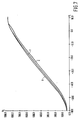
- Figure 7 shows a graph of the measured performance with temperature of a three stage logarithmic cascaded amplifier in accordance with the invention.
- the horizontal axis represents the input voltage Vi on a decibel scale and the vertical axis represents the output voltage Vo on a linear scale.
- the first curve X shows the transfer function of the amplifier at -20 o C
- the second curve Y shows the transfer function of the amplifier at 25 o C
- the third curve Z shows the transfer function of the amplifier at 75 o C.
- the transfer function of the amplifier varies very little with temperature. What is particularly significant is that in addition to successfully reducing a large variation in output limit voltage, the slight variation in the characteristic is only an input scale variation and not a slope variation. Consequently, accurate measurements of relative amplitude of signals applied to the amplifier are still available regardless of temperature.
- a three stage amplifier is considered.
- the three stages are arranged as shown in Figure 1 and each comprise a linear amplifier having gains of k1,k2 and k3 respectively and a limiting amplifier having gains of A1,A2 and A3 and limiting output voltages of L1,L2 and L3, respectively.
- the overall input voltage is Vi and the overall output voltage is Vo.
- the transfer function for the amplifier will have three knee points corresponding to the onset of limiting in the three limiting amplifiers and these points are relatively easy to define.
- VI3 L3 A3
- This equation gives the transfer function of the amplifier at the onset of limiting in the third amplifying stage. As the input voltage Vi increases, the limiting amplifier in the third stage provides no further gain but continues to provide its limited output voltage L3.
- VI2 L2 A2
- VI3 VI2.(A2+k2)
- the equations (1),(3),(5) give the stage input voltages for the onset of limiting in the three stages.
- the equations (2),(4),(6) give the transfer functions of the cascaded amplifier at these three onsets of limiting. By using these equations, the stage amplifier parameters for a very large variety of transfer functions can be derived.
- the procedure above can be repeated as necessary to derive transfer functions for cascaded amplifiers having more than three stages.
- the number of variables involved in the closed form determination of the amplifier parameters is prohibitive.
- the values of the variables can be constrained in a number of ways. Conveniently the limiting voltages of all of the limiting amplifiers may be constrained to be equal. Alternatively the sum (A+k) for each stage can be constrained to be equal while the individual values of An and kn are varied for each stage in accordance with the equations above and the desired transfer function. Other means for reducing the number of variables are available.
- an amplifier in accordance with the present invention may be arranged to provide a super-linear transfer function, that is a transfer function having a gain which increases with the magnitude of the input to the amplifier, as well as other generally non-linear transfer functions.
- the limiting amplifier in one or more stages is arranged to have a negative value of gain whose absolute value is less than the absolute value of the gain of the linear amplifier.
- the output of the limiting amplifier thus provides an effect which counters the output of the linear amplifier until the onset of limiting is reached.
- the gain of such an amplifier stage thus increases at input levels above the onset of limiting since the limiting amplifier is not then providing any negative slope gain.
- a cascaded amplifier composed solely of such stages will provide a super-linear transfer function.
- a cascaded amplifier comprised of a mixture of sub-linear and super-linear stages can be arranged to provide an overall amplifier transfer function having a particular non-linear transfer function.
- FIG. 5 shows a block schematic diagram of a radio receiver in accordance with the present invention.
- Radio signals having a large dynamic range are received by an antenna connected to a R.F. stage 80 which down converts the signals to an intermediate frequency and supplies them to a band-pass filter 82.
- the output of the filter 82 is fed to a cascaded logarithmic amplifier 84 as described above to reduce the dynamic range of the filtered signal and provide a compressed signal to an analogue to digital converter (ADC) 86.
- ADC analogue to digital converter
- the digitised output of the ADC is fed to a digital signal processor (DSP) 88 which provides demodulation for the digitised signal to provide an output signal at a terminal 90.
- DSP digital signal processor
- a zero IF architecture may be used which comprises in-phase and quadrature channels substantially at baseband.
Landscapes
- Engineering & Computer Science (AREA)
- Power Engineering (AREA)
- Microelectronics & Electronic Packaging (AREA)
- Amplifiers (AREA)
- Tone Control, Compression And Expansion, Limiting Amplitude (AREA)
Claims (7)
- Amplificateur en cascade comportant une pluralité d'étages d'amplification connectés en cascade, chaque étage d'amplification comprenant un amplificateur linéaire et un amplificateur limiteur, l'amplificateur linéaire et l'amplificateur limiteur étant pourvus d'un signal d'entrée d'étage et procurant des signaux de sortie respectifs qui sont combinés pour procurer un signal de sortie d'étage, caractérisé en ce que chaque étage d'amplification dans la cascade comporte en outre des moyens dépendant de la température pour commander le gain de petits signaux de cet étage d'amplification pour qu'il soit pratiquement indépendant de la température, et un étage final de l'amplificateur comporte des moyens dépendant de la température pour commander la tension limite de sortie totale de l'amplificateur en cascade pour qu'elle soit pratiquement indépendante de la température.
- Amplificateur suivant la revendication 1, dans lequel les moyens dépendant de la température de l'étage final d'amplification comprennent des moyens pour commander le gain de cet étage pour qu'il soit inversement proportionnel à la température absolue.
- Amplificateur suivant la revendication 2, dans lequel l'étage final d'amplification inclut un circuit translinéaire.
- Amplificateur suivant la revendication 3, comportant en outre une source de courant constante couplée à un circuit translinéaire.
- Amplificateur suivant l'une quelconque des revendications 1 à 4, comprenant en outre un amplificateur limiteur ayant une sortie couplée à un premier étage d'amplification en cascade.
- Amplificateur suivant l'une quelconque des revendications précédentes, dans lequel l'amplificateur linéaire de chaque étage d'amplification est agencé pour avoir un gain unité et l'amplificateur fournit une fonction de transfert pratiquement logarithmique.
- Récepteur radio comprenant un étage de fréquence radio incluant des moyens de changement de fréquence pour fournir un signal ayant subi un changement de fréquence à un amplificateur logarithmique comme revendiqué à la revendication 6, une sortie de l'amplificateur pratiquement logarithmiquement liée au signal ayant subi un changement de fréquence étant fournie à des moyens de numérisation pour fournir un signal numérique à un processeur numérique de signaux.
Applications Claiming Priority (2)
| Application Number | Priority Date | Filing Date | Title |
|---|---|---|---|
| GB9313840 | 1993-07-05 | ||
| GB939313840A GB9313840D0 (en) | 1993-07-05 | 1993-07-05 | Cascaded amplifier |
Publications (3)
| Publication Number | Publication Date |
|---|---|
| EP0633657A2 EP0633657A2 (fr) | 1995-01-11 |
| EP0633657A3 EP0633657A3 (fr) | 1996-01-31 |
| EP0633657B1 true EP0633657B1 (fr) | 2000-01-19 |
Family
ID=10738300
Family Applications (1)
| Application Number | Title | Priority Date | Filing Date |
|---|---|---|---|
| EP94201874A Expired - Lifetime EP0633657B1 (fr) | 1993-07-05 | 1994-06-29 | Amplificateur en cascade |
Country Status (7)
| Country | Link |
|---|---|
| US (1) | US5471173A (fr) |
| EP (1) | EP0633657B1 (fr) |
| JP (1) | JPH07106859A (fr) |
| KR (1) | KR100345586B1 (fr) |
| DE (1) | DE69422668T2 (fr) |
| GB (1) | GB9313840D0 (fr) |
| SG (1) | SG48400A1 (fr) |
Families Citing this family (20)
| Publication number | Priority date | Publication date | Assignee | Title |
|---|---|---|---|---|
| DE4416981A1 (de) * | 1994-05-13 | 1995-11-16 | Philips Patentverwaltung | Schaltungsanordnung mit einer Gesamtübertragungsfunktion |
| DE19518225C1 (de) * | 1995-05-11 | 1996-12-12 | Deutsche Forsch Luft Raumfahrt | Schaltungsanordnung zur Bildung der Quadratwurzel eines Eingangssignals |
| AU736045B2 (en) | 1996-10-22 | 2001-07-26 | Abb Inc. | Energy meter with power quality monitoring and diagnostic systems |
| US5903185A (en) * | 1996-12-20 | 1999-05-11 | Maxim Integrated Products, Inc. | Hybrid differential pairs for flat transconductance |
| US5946181A (en) * | 1997-04-30 | 1999-08-31 | Burr-Brown Corporation | Thermal shutdown circuit and method for sensing thermal gradients to extrapolate hot spot temperature |
| US5994961A (en) * | 1997-12-08 | 1999-11-30 | Motorola, Inc. | Temperature compensated decibel linear variable gain amplifier |
| KR100288939B1 (ko) * | 1998-02-10 | 2001-05-02 | 구자홍 | 현금지급기의명세표및저널용지처리장치 |
| US6020786A (en) * | 1998-08-03 | 2000-02-01 | Lucent Technologies Inc. | Temperature compensation for variable gain amplifiers |
| US6292057B1 (en) | 1998-12-18 | 2001-09-18 | Texas Instruments Incorporated | Output stage of an operational amplifier and method having a latchup-free sourcing current booster for driving low impedance loads |
| US6369618B1 (en) * | 1999-02-12 | 2002-04-09 | Texas Instruments Incorporated | Temperature and process independent exponential voltage-to-current converter circuit |
| US6664843B2 (en) | 2001-10-24 | 2003-12-16 | Institute Of Microelectronics | General-purpose temperature compensating current master-bias circuit |
| US7012343B2 (en) * | 2003-04-11 | 2006-03-14 | Micrel, Inc. | Resistance multiplier circuit and compact gain attenuator |
| US6980052B1 (en) | 2003-08-08 | 2005-12-27 | Linear Technology Corporation | Low-voltage pre-distortion circuit for linear-in-dB variable-gain cells |
| US6972624B1 (en) | 2003-08-08 | 2005-12-06 | Linear Technology Corporation | Low-voltage high dynamic range variable-gain amplifier |
| EP1555752A1 (fr) * | 2004-01-14 | 2005-07-20 | Dialog Semiconductor GmbH | Condensateur variable ayant un facteur de qualité élevé comprend un amplificateur translinéaire |
| US7262661B2 (en) | 2005-06-27 | 2007-08-28 | Linear Technology Corporation | Variable gain amplifier with temperature compensation and gain linearity enhancement |
| DE102006020485B4 (de) | 2006-04-28 | 2019-07-04 | Atmel Corp. | Operationsverstärker |
| US7288983B1 (en) | 2006-08-30 | 2007-10-30 | Broadlight Ltd. | Method and circuit for providing a temperature dependent current source |
| US7830134B2 (en) * | 2006-10-06 | 2010-11-09 | Ladybug Technologies Llc | Power meter with means to eliminate the need to zero and calibrating |
| IT202200005651A1 (it) * | 2022-03-22 | 2023-09-22 | St Microelectronics Srl | Disposizione circuitale di amplificatore con controllo di guadagno in corrente e corrispondente procedimento |
Family Cites Families (5)
| Publication number | Priority date | Publication date | Assignee | Title |
|---|---|---|---|---|
| JPS58114617A (ja) * | 1981-12-28 | 1983-07-08 | テクトロニツクス・インコ−ポレイテツド | 非直線増幅器 |
| CA1203628A (fr) * | 1983-01-03 | 1986-04-22 | Barrie Gilbert | Circuit logarithmique a compensation des effets dus a la temperature |
| US4604532A (en) * | 1983-01-03 | 1986-08-05 | Analog Devices, Incorporated | Temperature compensated logarithmic circuit |
| US4990803A (en) * | 1989-03-27 | 1991-02-05 | Analog Devices, Inc. | Logarithmic amplifier |
| EP0517305B1 (fr) * | 1991-06-03 | 1995-11-22 | Koninklijke Philips Electronics N.V. | Amplificateur et détecteur logarithmique |
-
1993
- 1993-07-05 GB GB939313840A patent/GB9313840D0/en active Pending
-
1994
- 1994-06-29 SG SG1996009387A patent/SG48400A1/en unknown
- 1994-06-29 EP EP94201874A patent/EP0633657B1/fr not_active Expired - Lifetime
- 1994-06-29 DE DE69422668T patent/DE69422668T2/de not_active Expired - Fee Related
- 1994-06-30 US US08/269,811 patent/US5471173A/en not_active Expired - Fee Related
- 1994-07-04 JP JP6152188A patent/JPH07106859A/ja active Pending
- 1994-07-05 KR KR1019940015961A patent/KR100345586B1/ko not_active IP Right Cessation
Also Published As
| Publication number | Publication date |
|---|---|
| US5471173A (en) | 1995-11-28 |
| KR100345586B1 (ko) | 2002-12-05 |
| GB9313840D0 (en) | 1993-08-25 |
| EP0633657A2 (fr) | 1995-01-11 |
| JPH07106859A (ja) | 1995-04-21 |
| EP0633657A3 (fr) | 1996-01-31 |
| DE69422668T2 (de) | 2000-08-10 |
| KR950004723A (ko) | 1995-02-18 |
| DE69422668D1 (de) | 2000-02-24 |
| SG48400A1 (en) | 1998-04-17 |
Similar Documents
| Publication | Publication Date | Title |
|---|---|---|
| EP0633657B1 (fr) | Amplificateur en cascade | |
| EP0636288B1 (fr) | Amplificateur logarithmique de demodulation | |
| US5886579A (en) | Variable gain CMOS amplifier | |
| US5418494A (en) | Variable gain amplifier for low supply voltage systems | |
| US20030112072A1 (en) | Exponential function generator embodied by using a CMOS process and variable gain amplifier employing the same | |
| Meyer et al. | A DC to 1-GHz differential monolithic variable-gain amplifier | |
| EP0004099B1 (fr) | Circuit d'impédance à commande électrique | |
| AU706648B2 (en) | Temperature compensated logarithmic convertor | |
| GB2250649A (en) | Temperature compensation control circuit for exponential gain function of an AGO amplifier | |
| KR940005376B1 (ko) | 이득가변증폭기 | |
| US4495429A (en) | Limiter amplifier | |
| US6456142B1 (en) | Circuit having dual feedback multipliers | |
| CA2062010C (fr) | Circuit d'amplification logarithmique | |
| US5587689A (en) | Voltage controlled amplifier with a negative resistance circuit for reducing non-linearity distortion | |
| US4724337A (en) | Automatic gain control detection circuit | |
| JPH09502316A (ja) | デシベル−線形出力電圧を有する増幅器段 | |
| US6028478A (en) | Converter circuit and variable gain amplifier with temperature compensation | |
| EP0114731A1 (fr) | Amplificateur différentiel assurant un taux élevé de réjection de mode commun | |
| JP3476521B2 (ja) | 受信信号強度表示器を有する装置と対数検出器を含む電子回路 | |
| JP2885281B2 (ja) | Dcオフセットキャンセル回路及びそれを用いた差動増幅回路 | |
| EP0730345B1 (fr) | Circuit à gain variable | |
| US5631594A (en) | Tunable logarithmic amplifier circuit using cascaded triple-tail cells | |
| JPS5820482B2 (ja) | 増巾器 | |
| US7310656B1 (en) | Grounded emitter logarithmic circuit | |
| US4538300A (en) | Linear signal strength detector in AM radio |
Legal Events
| Date | Code | Title | Description |
|---|---|---|---|
| PUAI | Public reference made under article 153(3) epc to a published international application that has entered the european phase |
Free format text: ORIGINAL CODE: 0009012 |
|
| AK | Designated contracting states |
Kind code of ref document: A2 Designated state(s): DE FR GB IT |
|
| PUAL | Search report despatched |
Free format text: ORIGINAL CODE: 0009013 |
|
| AK | Designated contracting states |
Kind code of ref document: A3 Designated state(s): DE FR GB IT |
|
| 17P | Request for examination filed |
Effective date: 19960731 |
|
| GRAG | Despatch of communication of intention to grant |
Free format text: ORIGINAL CODE: EPIDOS AGRA |
|
| 17Q | First examination report despatched |
Effective date: 19990331 |
|
| GRAG | Despatch of communication of intention to grant |
Free format text: ORIGINAL CODE: EPIDOS AGRA |
|
| GRAH | Despatch of communication of intention to grant a patent |
Free format text: ORIGINAL CODE: EPIDOS IGRA |
|
| GRAH | Despatch of communication of intention to grant a patent |
Free format text: ORIGINAL CODE: EPIDOS IGRA |
|
| GRAA | (expected) grant |
Free format text: ORIGINAL CODE: 0009210 |
|
| AK | Designated contracting states |
Kind code of ref document: B1 Designated state(s): DE FR GB IT |
|
| REF | Corresponds to: |
Ref document number: 69422668 Country of ref document: DE Date of ref document: 20000224 |
|
| ITF | It: translation for a ep patent filed |
Owner name: ING. C. GREGORJ S.P.A. |
|
| ET | Fr: translation filed | ||
| PLBE | No opposition filed within time limit |
Free format text: ORIGINAL CODE: 0009261 |
|
| STAA | Information on the status of an ep patent application or granted ep patent |
Free format text: STATUS: NO OPPOSITION FILED WITHIN TIME LIMIT |
|
| 26N | No opposition filed | ||
| REG | Reference to a national code |
Ref country code: GB Ref legal event code: IF02 |
|
| PGFP | Annual fee paid to national office [announced via postgrant information from national office to epo] |
Ref country code: FR Payment date: 20030625 Year of fee payment: 10 |
|
| PGFP | Annual fee paid to national office [announced via postgrant information from national office to epo] |
Ref country code: GB Payment date: 20030627 Year of fee payment: 10 |
|
| PGFP | Annual fee paid to national office [announced via postgrant information from national office to epo] |
Ref country code: DE Payment date: 20030818 Year of fee payment: 10 |
|
| PG25 | Lapsed in a contracting state [announced via postgrant information from national office to epo] |
Ref country code: GB Free format text: LAPSE BECAUSE OF NON-PAYMENT OF DUE FEES Effective date: 20040629 |
|
| PG25 | Lapsed in a contracting state [announced via postgrant information from national office to epo] |
Ref country code: DE Free format text: LAPSE BECAUSE OF NON-PAYMENT OF DUE FEES Effective date: 20050101 |
|
| GBPC | Gb: european patent ceased through non-payment of renewal fee |
Effective date: 20040629 |
|
| PG25 | Lapsed in a contracting state [announced via postgrant information from national office to epo] |
Ref country code: FR Free format text: LAPSE BECAUSE OF NON-PAYMENT OF DUE FEES Effective date: 20050228 |
|
| REG | Reference to a national code |
Ref country code: FR Ref legal event code: ST |
|
| PG25 | Lapsed in a contracting state [announced via postgrant information from national office to epo] |
Ref country code: IT Free format text: LAPSE BECAUSE OF NON-PAYMENT OF DUE FEES;WARNING: LAPSES OF ITALIAN PATENTS WITH EFFECTIVE DATE BEFORE 2007 MAY HAVE OCCURRED AT ANY TIME BEFORE 2007. THE CORRECT EFFECTIVE DATE MAY BE DIFFERENT FROM THE ONE RECORDED. Effective date: 20050629 |