EP0632563B1 - Standby-Schaltung für elektrische Verbraucher - Google Patents
Standby-Schaltung für elektrische Verbraucher Download PDFInfo
- Publication number
- EP0632563B1 EP0632563B1 EP94110111A EP94110111A EP0632563B1 EP 0632563 B1 EP0632563 B1 EP 0632563B1 EP 94110111 A EP94110111 A EP 94110111A EP 94110111 A EP94110111 A EP 94110111A EP 0632563 B1 EP0632563 B1 EP 0632563B1
- Authority
- EP
- European Patent Office
- Prior art keywords
- switched
- power supply
- detector
- detector device
- decoder
- Prior art date
- Legal status (The legal status is an assumption and is not a legal conclusion. Google has not performed a legal analysis and makes no representation as to the accuracy of the status listed.)
- Expired - Lifetime
Links
Images

Classifications
-
- H—ELECTRICITY
- H02—GENERATION; CONVERSION OR DISTRIBUTION OF ELECTRIC POWER
- H02J—ELECTRIC POWER NETWORKS; CIRCUIT ARRANGEMENTS OR SYSTEMS FOR SUPPLYING OR DISTRIBUTING ELECTRIC POWER; SYSTEMS FOR STORING ELECTRIC ENERGY
- H02J9/00—Circuit arrangements for emergency or stand-by power supply, e.g. for emergency lighting
- H02J9/005—Circuit arrangements for emergency or stand-by power supply, e.g. for emergency lighting using a power saving mode
-
- Y—GENERAL TAGGING OF NEW TECHNOLOGICAL DEVELOPMENTS; GENERAL TAGGING OF CROSS-SECTIONAL TECHNOLOGIES SPANNING OVER SEVERAL SECTIONS OF THE IPC; TECHNICAL SUBJECTS COVERED BY FORMER USPC CROSS-REFERENCE ART COLLECTIONS [XRACs] AND DIGESTS
- Y02—TECHNOLOGIES OR APPLICATIONS FOR MITIGATION OR ADAPTATION AGAINST CLIMATE CHANGE
- Y02B—CLIMATE CHANGE MITIGATION TECHNOLOGIES RELATED TO BUILDINGS, e.g. HOUSING, HOUSE APPLIANCES OR RELATED END-USER APPLICATIONS
- Y02B70/00—Technologies for an efficient end-user side electric power management and consumption
- Y02B70/30—Systems integrating technologies related to power network operation and communication or information technologies for improving the carbon footprint of the management of residential or tertiary loads, i.e. smart grids as climate change mitigation technology in the buildings sector, including also the last stages of power distribution and the control, monitoring or operating management systems at local level
-
- Y—GENERAL TAGGING OF NEW TECHNOLOGICAL DEVELOPMENTS; GENERAL TAGGING OF CROSS-SECTIONAL TECHNOLOGIES SPANNING OVER SEVERAL SECTIONS OF THE IPC; TECHNICAL SUBJECTS COVERED BY FORMER USPC CROSS-REFERENCE ART COLLECTIONS [XRACs] AND DIGESTS
- Y04—INFORMATION OR COMMUNICATION TECHNOLOGIES HAVING AN IMPACT ON OTHER TECHNOLOGY AREAS
- Y04S—SYSTEMS INTEGRATING TECHNOLOGIES RELATED TO POWER NETWORK OPERATION, COMMUNICATION OR INFORMATION TECHNOLOGIES FOR IMPROVING THE ELECTRICAL POWER GENERATION, TRANSMISSION, DISTRIBUTION, MANAGEMENT OR USAGE, i.e. SMART GRIDS
- Y04S20/00—Management or operation of end-user stationary applications or the last stages of power distribution; Controlling, monitoring or operating thereof
- Y04S20/20—End-user application control systems
Definitions
- the invention relates to a standby circuit for electrical Consumers containing a decoder device through which signal sent by the remote control is decoded, and a power supply for the consumer who is turned on when by the decoder device Command to switch on the power supply detected becomes.
- Standby circuits are circuits for electrical consumers, which are kept in operation while the rest Functional units of the consumer are switched off from a remote control to receive signals and that Turn on device when a signal identifier for turn on is detected. Since a standby circuit is constantly in Operation is, it should be implemented in such a way that it is as possible consumed little power loss.
- the switching power supply essentially contains a transformer, a switching device through which the Current flow through the transformer on and off is, and a device for controlling the switching device.
- the control device has a standby mode in which essentially only the infrared receiving and secondary winding output feeding decoder is in operation while the other circuit parts the winding outputs supplying the device at idle operate. Since the control device and the corresponding Part of the transformer during the standby phase are constantly on, a relatively high power loss consumes that are usually of the order of magnitude of 10 watts.
- the consumer is another Transformer provided by the remote control receiver is fed. During standby mode, this will be Switched-mode power supply switched off. The additional transformer and the remote control receiver are switched on continuously. Also with today's developments of this principle lies the Total power loss essentially due to that in the transformer power consumed about the order of 1 Watt.
- EP 0 158 251 B2 describes a circuit arrangement for the Standby operation of a television receiver described the one Switching power supply.
- This switching power supply is on the primary side an amplifier for remote control signals and secondary is an evaluation circuit on this switching power supply (Decoder) connected.
- the secondary-side Evaluation circuit is switched off.
- Will be from Amplifier receives a remote control signal, that will Switched-mode power supply activated to switch on the evaluation circuit.
- the amplified remote control signal becomes galvanic Transfer separation from primary to secondary, which requires an effort in discrete components and why the primary-side amplifier also a relatively high Must provide output power.
- the object of the invention is that specified at the outset Standby operating circuit so that they the lowest possible power loss during standby mode having.
- the detector In the standby mode only the detector is permanent switched on.
- the decoder is normally switched off and turns on only when receiving a remote control signal.
- the circuit for the detector can be implemented with high resistance become. Thus, a low continuous power consumption is Standby mode guaranteed.
- the detector and decoder are separate on the primary or secondary side of the Transformer arranged.
- the detector can consist of one Energy storage can be supplied.
- the capacitor When using a capacitor recharging the capacitor is an energy store if the minimum voltage falls below the Start-up operation of the switching power supply necessary.
- a rechargeable battery As an energy storage device Charging takes place when the consumer is started up.
- the detector can be divided by voltage division and Rectification in the current path of the Y capacitors arranged on the primary side be supplied with power.
- a standby circuit contains a power supply device 1, for example a power converter, in particular a switching power supply can.
- the switching power supply 1 is switched on Rectification, e.g. B. by a bridge rectifier, obtained DC voltage supplied.
- At least one Secondary output 8 of the switching power supply 1 is on one other voltage level converted DC voltage for operation of functional units of the consumer.
- a secondary output 7 becomes a control unit 2 Power supplied.
- the control unit 2 contains at least a decoder device 3 through which a remote control emitted signal, usually an infrared signal, decoded and corresponding control signals is implemented.
- the remote control signal contains, among other things Commands for switching the consumer on and off.
- a detector device 4 becomes the reception of an infrared signal detected. One in the infrared signal, if applicable The command contained therein is ignored. If from Detector 4 an infrared signal is detected, the Facility 2 switched on. This can be done by appropriate Circuit measures for switching on in the facility 2 be carried out by yourself or by activating the corresponding power supply output 7 of the switching power supply 1. The switched on decoder 3 of the control device 2 then decodes the one sent by the remote control Signal. For this purpose there is another one in device 2 Infrared receiver and preamplifier provided, the Output signal is fed into the decoder 3.
- the facilities 3, 4 can both from the primary side and from the Secondary side of the switching power supply 1 supplied with power become.
- the detector 4 on the primary side Decoder 3 arranged on the secondary side of the switching power supply become.
- the corresponding embodiments are in Figures 2 to 5 shown. Signals from the Primary side on the secondary side of the switching power supply 1 are always galvanically decoupled. This can be done, for example, by a transformer or a Combination of light emitting diode and photo transistor can be effected.
- the detector 4 is on the primary side of the Switching power supply 1, the decoder 3 on the secondary side.
- the Switching power supply 1 contains a transformer 10, in the Primary winding, a switching transistor 11 is connected.
- the Switching transistor 11 chops the current flow through the primary winding of the transformer 10, passing through a device 12 is controlled.
- the device 12 is common an integrated circuit.
- the switching power supply 1 becomes the primary side at a connection 14 from a rectified Mains voltage, which is based on primary mass 13, supplied.
- the decoder 4 is also from the rectified mains voltage supplied at connection 14.
- An output 15 of the decoder 4 is with a corresponding input of the control IC 12 of the switching power supply 1, so that the switching power supply 1 is switched on with an active signal at connection 15.
- the switching power supply 1 is expediently in one Operating mode in which only the one described below Control device 2 is turned on while others Functional units of the consumer are still switched off are. This operating mode of the switching power supply is off the prior art mentioned at the outset.
- the standby circuit also contains the control device 2 by a secondary winding 16 of the transformer 10 of the switching power supply 1 is supplied.
- the control device 2 contains the decoder 3 and an infrared preamplifier 9. After the switching power supply 1 is present of an infrared signal has been turned on, the infrared signal also received by the preamplifier 9, the signal amplified and feeds the decoder 3. In dependence of the command decoded from the infrared signal is controlled by the Decoder 3 the standby circuit. Contains the infrared signal no decodable command if e.g. B. an infrared signal from a remote control not belonging to the consumer is received, the switching power supply 1 again off.
- connection 18 is provided, for example with a Switch-on contact, e.g. B. a wiping contact is connected.
- the detector 4 remains switched on continuously. He can can be realized with high impedance, so that little power loss is consumed.
- the switched-on power supply 1 and the Control device 2, whose decoder 3 is usually a Complex integrated circuit is compared to consume with the detector 4 a relatively high power loss. You will therefore only see an infrared signal switched on. Thus, the power loss remains Overall circuit in standby mode compared to conventional Solutions relatively minor.
- the decoder 3 is on the Primary side of the switching power supply 1 is arranged.
- the decoder 3 is switched on. This can be achieved, for example, by that the decoder 3 is supplied with voltage through the connection 15 becomes.
- the decoder 3 is also via an output 21 of the Detector 4, the received and amplified infrared signal 21 fed. If a signal to switch on the consumer is recognized by the decoder 3, is via its output 22nd the switching power supply 1 and thus the consumer switched on.
- the output 22 is corresponding to the input 17 of the Detector 4 fed back to decoder 3 for decoding to keep a shutdown command on.
- the decoder 3 can low circuitry and thus low power consumption will be realized.
- its supply is via the Output 15 of the detector 4 is easily possible.
- the decoding further control functions is from another Decoder running from the secondary side of the Switch power supply 1 is supplied and only when switching on of the consumer is activated.
- the arrangement of the decoder 3 on the primary side achieved that the switching power supply 1 is only switched on is when an infrared signal to turn on from the to Remote control belonging to the consumer is received. All other infrared signals have no effect on the switching power supply 1.
- the one contained in the switching power supply 1 Control circuit compared to the embodiment according to 1 shows no extra operating mode for supplying the secondary side Infrared receiver and decoder. advantageously, can that applied to the output 21 of the detector 4 amplified infrared signal without significant circuitry at an internal circuit node of the detector 4 be tapped.
- the detector 4 shows an embodiment in which both the detector 4 and the decoder 3 on the secondary side of the switching power supply 1 are arranged.
- the detector 4 will for power supply during the standby phase from one Energy storage supplied. In the present case it is Energy storage a capacitor 34 from the secondary side of the switching power supply 1 is charged.
- the decoder 3 is switched off so that it does not consume any electricity. By the current requirement of the detector 4 becomes the capacitor 34 discharged. If the voltage drops below a minimum, Signal at an output 35 of detector 4 switched active, which via an optocoupler 31 on the primary side of the Switching power supply 1 is coupled and the switching power supply 1 so long turns on until the capacitor 34 is back on its is fully charged. This is generally sufficient the start-up operation of the switching power supply 1.
- the one at the exit 35 of the detector 4 applied signal can without essential Circuit effort at an internal circuit node of the Detector 4 can be tapped.
- the decoder 3 is switched off Expediently causes that through the terminal 15th the clock of the circuit 3 is switched off.
- the decoder 3 is switched on when an infrared signal from the detector 4 is recognized. This is the decoder 3 via the output 21 of the detector 4 fed increasingly. Decoder 3 switches when detecting a signal to switch on the Consumer output 32 active, which also on the Primary side of the switching power supply 1 is fed back. there the outputs 32, 35 of the decoder 3 or detector 4 in Switching element 30 OR-linked.
- the switching power supply 1 is only for charging of the capacitor 34 briefly switched on in the start-up mode. As a result, the power loss is low. Also for that Switching power supply 1 no standby mode setting required.
- Capacitor 34 can also use a rechargeable battery become. It is assumed that the battery capacity is sufficient to supply the detector 4 with current supply until the device is switched on. Only then will the battery is recharged.
- a primary supply can also be provided.
- the corresponding version of this power supply is in 5 shown.
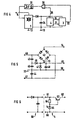
- the applied to connections 40, 41 Mains AC voltage is in a bridge rectifier circuit 42 rectified and is at port 14 with respect Primary mass 13 before.
- interference suppression is between the connections 40, 41 two capacitors connected in series 43, 44 provided whose connection point with Secondary ground, that is, the ground terminal 33 is connected.
- the Capacitors 43, 44 are commonly called Y capacitors designated. According to the invention is between the capacitor 43 and the secondary ground connection 33 for voltage division Alternating circuit switched a capacitor 45.
- the one on the capacitor 45 AC voltage is applied via a rectifier network from diodes 46, 47 and a capacitor 48 rectified and smoothed.
- the voltage across capacitor 48 is therefore available with regard to the secondary mass 33.
- To the connection terminals 49, 50 of the capacitor 48 becomes the secondary side working detector 4 connected to the power supply.
- the power supply shown in FIG 5 for the detector 4 can be implemented with little circuitry complexity. Since the detector 4 has a low power consumption and with appropriate dimensioning with a low supply voltage can be fed is the requirement regarding the dielectric strength to the capacitor 45 comparatively low.
- the infrared detector 4 has a connection 60 for a reference potential and a supply connection 61. Between the Terminal 61 and an output terminal 62 is the emitter-collector path a pnp bipolar transistor 63rd base and The emitters of transistor 63 are via a resistor 64 connected. The base of transistor 63 is one for Diode 65 sensitive to infrared light with reference terminal 60 connected. The diode 65 provides for increasing illuminance an increasing reverse current.
- the pair of input terminals 60, 61 is connected to a DC supply voltage. For connection to an AC voltage, a Diode-capacitor rectifier circuit 66 used become.
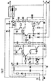
- FIG. 1 A detailed circuit diagram of a detector that has a high Reinforcement and high-pass character and therefore special Suitable for standard infrared signals from a remote control is shown in FIG.
- the detector contains on the input side a rectification and smoothing element 66. Die input-side terminals 60, 72 can be connected to both AC voltage as well as connected to a DC voltage become.
- the photodiode 65 is one with the center connection Voltage divider 71a, 71b connected. This is the Protected photodiode 65 from high reverse voltages.
- To the A capacitor 73 is connected to the cathode of the photodiode 65.
- the capacitor 73 acts as a high-pass filter, so that only fast changing brightness signals, as usually from Infrared transmitters are broadcast, processed.
- the Circuit thus remains exposed to fluctuations in brightness Daylight or low frequency modulated light insensitive to light bulbs.
- the capacitor 73 is a first amplifier stage 67 is connected on the output side, which in turn is followed by a second amplifier stage 68.
- the amplifier stage 68 contains a Darlington circuit on the output side 76, which ensures a high gain.
- the amplifier circuit 68 has a high-pass character. Due to the overall gain of the series
- the detector also has amplifiers 67, 68 for weak ones incoming infrared signals sufficient high gain.
- the Circuits 69, 70 ensure independent adjustment and Stabilization of the working point, so that a comparison of the Circuit is not necessary.
- the output of amplifier 68 switches the pnp bipolar transistor 63.
- the collector terminal 62 controls the excitation winding of a relay 77. This indicates the output 15 of the detector has sufficient current driving capability on.
- the amplifier stage 68 connected capacitor 80 Through the output side the amplifier stage 68 connected capacitor 80, the together with the resistors 64, 82, 83 of the as Integrator acts, can for the switching function of the A suitable inertia to be selected by the detector, so that with a short, possibly disturbed reception signal transistor 63 is not switched.
- Signal input 17 for a switch-on contact and the signal input 18 for the Feedback attack on the circuit node 81 which with the Base of the Darlington circuit 76 is connected.
- At node 81 can be coupled another input, not shown be connected to a timer.
- This The timer is used for time-controlled devices Detector and one controlled by the detector Turn on the control device for a short time, by the then it is determined whether there is a time condition for turning on of the device.
- the detector according to FIG. 7 can be used both with equal and with AC voltage operated.
- When operating on the A supply is recommended for the primary side of the switching power supply with a voltage equal to the mains voltage.
- a supply voltage is advantageous, which are also integrated for the operation of digital Circuits (e.g. 5 V) is suitable.
- the circuit shown can be used with suitable dimensions of the Components for different supply voltage levels be used.
- the power consumption lies in Milliwatt range.
- the circuit can easily be called integrated circuit can be realized. It can be used as an infrared amplifier and detector for others, not related applications with standby circuits become.
Landscapes
- Business, Economics & Management (AREA)
- Emergency Management (AREA)
- Engineering & Computer Science (AREA)
- Power Engineering (AREA)
- Selective Calling Equipment (AREA)
- Direct Current Feeding And Distribution (AREA)
Description
- FIG 1
- ein Prinzipschaltbild einer erfindungsgemäßen Standby-Schaltung,
- FIG 2
- eine Ausführung mit primärseitiger Anordnung des Detektors und sekundärseitiger Anordnung des Dekoders,
- FIG 3
- eine Ausführung mit primärseitiger Anordnung von Detektor und Dekoder,
- FIG 4
- eine Ausführung mit sekundärseitiger Anordnung von Detektor und Dekoder,
- FIG 5
- die Leistungsversorgung des Detektors bei sekundärseitiger Anordnung entsprechend FIG 4,
- FIG 6
- das Prinzipschaltbild eines Detektors und
- FIG 7
- eine Ausführung des Detektors im Detail.
Claims (8)
- Standby-Schaltung für elektrische Verbraucher enthaltend eine Detektoreinrichtung (4), durch die ein von einer Fernbedienung ausgesandtes Signal empfangbar ist, eine Dekodereinrichtung (3), durch die das von der Fernbedienung ausgesandte Signal dekodiert wird und die während einer Standby-Phase abgeschaltet ist und eingeschaltet wird, wenn von der Detektoreinrichtung (4) ein empfangenes Signal festgestellt wird, und eine Leistungsversorgung für den Verbraucher, die eingeschaltet wird, wenn durch die Dekodereinrichtung (3) ein Befehl zum Einschalten der Leistungsversorgung festgestellt wird, mit einem Leistungsumsetzer (1), von dessen Primärseite die Detektoreinrichtung (4) und von dessen Sekundärseite die Dekodereinrichtung (3) versorgt werden und der beim Feststellen des empfangenen Signals durch die Detektoreinrichtung (4) in einen Zustand geschaltet wird, bei dem die Dekodereinrichtung (3) mit Leistung versorgt wird,
dadurch gekennzeichnet, daß
eine weitere Detektoreinrichtung (9), durch die ein von der Fernbedienung ausgesandtes Signal empfangbar ist, von der Sekundärseite des Leistungsumsetzers (1) versorgt wird und daß ein Ausgangssignal der weiteren Detektoreinrichtung (9) der Dekodereinrichtung (3) zur Dekodierung zugeführt wird. - Standby-Schaltung nach Anspruch 1,
dadurch gekennzeichnet, daß die Detektoreinrichtung (3) von einem Energiespeicher (34) versorgt wird, der von der Sekundärseite des Leistungsumsetzers (1) wiederaufgeladen wird. - Standby-Schaltung nach Anspruch 2,
dadurch gekennzeichnet, daß der Energiespeicher ein Kondensator (34) ist, daß die Detektoreinrichtung (4) ein Spannungsüberwachungssignal erzeugt, durch das der die Detektoreinrichtung (4) speisende Teil des Leistungsumsetzers (1) eingeschaltet wird, wenn eine Mindestspannung unterschritten wird, und durch das der Leistungsumsetzer (1) ausschaltbar ist, wenn eine Sollspannung erreicht wird. - Standby-Schaltung nach Anspruch 1,
dadurch gekennzeichnet, daß die Detektoreinrichtung (3) durch einen Spannungsteiler (43, 44, 45) und durch eine Gleichrichtereinrichtung (46, 47, 48) aus einem Strompfad gespeist wird, der zwischen den Anschluß für eine
in die Primärseite des Leistungsumsetzers (1) eingespeiste Wechselspannung und einen Bezugsanschluß (33) der Sekundärseite des Leistungsumsetzers (1) geschaltet ist. - Standby-Schaltung nach einem der Ansprüche 1 bis 4,
dadurch gekennzeichnet, daß die Detektoreinrichtung (4) enthält:einen Bipolartransistor (63), dessen Emitter-Kollektor-Strecker zwischen einen Eingangsanschluß (61) und einen Ausgangsanschluß (62) geschaltet ist,ein zwischen Emitter und Basis des Bipolartransistors (63) geschaltetes Widerstandselements (64) undein lichtempfindliches Schaltelement (65), das einen ersten Anschluß für ein Bezugspotential aufweist und einen zweiten Anschluß, der mit der Basis des Bipolartransistors (63) gekoppelt ist. - Standby-Schaltung nach Anspruch 5,
dadurch gekennzeichnet, daß die Detektoreinrichtung (3) mindestens eine Signalverstärkereinrichtung (67, 68) mit Hochpaßeigenschaft enthält, deren Eingangs-Ausgangs-Signalpfad zwischen den zweiten Anschluß des lichtempfindlichen Schaltelements (65) und die Basis des Bipolartransistors (63) geschaltet ist. - Standby-Schaltung nach Anspruch 6,
dadurch gekennzeichnet, daß ein Integrierglied (82, 83, 80) zwischen die Basis des Bipolartransistors (63) und den Anschluß für das Bezugspotential (60) geschaltet ist. - Standby-Schaltung nach einem der Ansprüche 1 bis 4,
dadurch gekennzeichnet, daß der Leistungsumsetzer (1) ein Schaltnetzteil ist, der eine Steuerungseinrichtung (12) zur Steuerung der Betriebszustände des Schaltnetzteils und einen Transformator (10) enthält.
Applications Claiming Priority (2)
| Application Number | Priority Date | Filing Date | Title |
|---|---|---|---|
| DE4321948 | 1993-07-01 | ||
| DE4321948A DE4321948C3 (de) | 1993-07-01 | 1993-07-01 | Standby-Schaltung für elektrische Verbraucher |
Publications (4)
| Publication Number | Publication Date |
|---|---|
| EP0632563A2 EP0632563A2 (de) | 1995-01-04 |
| EP0632563A3 EP0632563A3 (de) | 1995-04-26 |
| EP0632563B1 true EP0632563B1 (de) | 2002-10-02 |
| EP0632563B2 EP0632563B2 (de) | 2008-07-09 |
Family
ID=6491731
Family Applications (1)
| Application Number | Title | Priority Date | Filing Date |
|---|---|---|---|
| EP94110111A Expired - Lifetime EP0632563B2 (de) | 1993-07-01 | 1994-06-29 | Standby-Schaltung für elektrische Verbraucher |
Country Status (2)
| Country | Link |
|---|---|
| EP (1) | EP0632563B2 (de) |
| DE (2) | DE4321948C3 (de) |
Families Citing this family (12)
| Publication number | Priority date | Publication date | Assignee | Title |
|---|---|---|---|---|
| DE19503243C2 (de) * | 1995-02-02 | 2000-08-03 | Loewe Opta Gmbh | Schaltungsanordnung |
| DE19540077A1 (de) * | 1995-10-27 | 1997-04-30 | Nokia Deutschland Gmbh | Fernbedienbare Videogeräteanordnung |
| DE19545659A1 (de) * | 1995-12-07 | 1997-06-12 | Thomson Brandt Gmbh | Schaltnetzteil für Normalbetrieb und Bereitschaftsbetrieb |
| DE19616726A1 (de) * | 1996-04-26 | 1997-10-30 | Thomson Brandt Gmbh | Anordnung zur Abschaltung der Netzspannung eines elektrischen Gerätes |
| WO1998001994A1 (de) * | 1996-07-04 | 1998-01-15 | Kuenzle Urs | Stromsparschaltung für ein elektronisches gerät und verfahren zur steuerung derselben |
| NL1009965C2 (nl) * | 1998-08-28 | 2000-02-29 | Bol Brothers Car Innovations C | Op afstand bedienbare schakelaar. |
| WO2000036830A1 (de) * | 1998-12-11 | 2000-06-22 | Siemens Ag Österreich | Stromlose standby-schaltung für geräte mit optischer fernbedienung |
| JP3188875B2 (ja) * | 1998-12-16 | 2001-07-16 | セイコーインスツルメンツ株式会社 | 電源回路 |
| US6525666B1 (en) | 1998-12-16 | 2003-02-25 | Seiko Instruments Inc. | Power circuit |
| IT1316251B1 (it) * | 2000-12-01 | 2003-04-03 | Elettronica G & C Snc Di Cella | Dispositivo interruttore di rete automatico. |
| ITTO20090214A1 (it) | 2009-03-20 | 2010-09-21 | St Microelectronics Srl | Circuito di alimentazione per l'accensione da remoto di apparecchi elettrici |
| US9118250B2 (en) | 2009-03-20 | 2015-08-25 | Stmicroelectronics S.R.L. | Power supply circuit for remotely turning-on electrical appliances |
Family Cites Families (12)
| Publication number | Priority date | Publication date | Assignee | Title |
|---|---|---|---|---|
| DE2503568A1 (de) * | 1975-01-29 | 1976-08-05 | Koerting Radio Werke Gmbh | Abschaltautomatik an funkempfaengern |
| DE2620191C2 (de) * | 1976-05-07 | 1982-05-06 | Graetz Gmbh & Co Ohg, 5990 Altena | Schaltnetzteil für die Versorgung eines Fernsehgerätes |
| DE3045715C2 (de) * | 1980-12-04 | 1986-01-16 | Loewe Opta Gmbh, 8640 Kronach | Fernsteuerbares nachrichtentechnisches Gerät |
| DE3231581A1 (de) * | 1981-09-17 | 1983-03-31 | Siemens AG, 1000 Berlin und 8000 München | Verfahren zum abschalten des standby-betriebs eines fernsehempfaengers |
| DE3234763A1 (de) * | 1982-09-20 | 1984-03-22 | Siemens AG, 1000 Berlin und 8000 München | Fernbedienbarer schalter |
| DE3303114C2 (de) * | 1983-01-31 | 1985-08-29 | Telefunken Fernseh Und Rundfunk Gmbh, 3000 Hannover | Selbstschwingendes Schaltnetzteil für ein Gerät mit Bereitschaftsbetrieb, insbesondere einen Fernsehempfänger |
| DE3412341C1 (de) * | 1984-04-03 | 1991-08-29 | Deutsche Thomson-Brandt Gmbh, 7730 Villingen-Schwenningen | Schaltungskonzept fuer den stand-by-Betrieb eines Fernsehempfaengers |
| DE3808863A1 (de) * | 1988-03-17 | 1989-09-28 | Philips Patentverwaltung | Stromversorgungsanordnung |
| DE3827210A1 (de) † | 1988-08-11 | 1990-02-15 | Grundig Emv | Fernbedienung fuer ein mit schaltnetzteil ausgeruestetes elektronisches geraet |
| JPH0616601B2 (ja) * | 1988-09-07 | 1994-03-02 | 三洋電機株式会社 | 受信電波処理回路のパワーセイブ回路及びそのパワーセイブ方法 |
| GB9000238D0 (en) * | 1990-01-05 | 1990-03-07 | Rca Licensing Corp | Minimum power standby circuit arrangement |
| DE9309814U1 (de) * | 1993-07-01 | 1993-09-02 | Siemens AG, 80333 München | Standby-Schaltung für elektrische Verbraucher |
-
1993
- 1993-07-01 DE DE4321948A patent/DE4321948C3/de not_active Expired - Fee Related
-
1994
- 1994-06-29 EP EP94110111A patent/EP0632563B2/de not_active Expired - Lifetime
- 1994-06-29 DE DE59410190T patent/DE59410190D1/de not_active Expired - Fee Related
Also Published As
| Publication number | Publication date |
|---|---|
| EP0632563A3 (de) | 1995-04-26 |
| DE4321948C3 (de) | 1999-02-25 |
| DE4321948A1 (de) | 1995-01-19 |
| EP0632563A2 (de) | 1995-01-04 |
| EP0632563B2 (de) | 2008-07-09 |
| DE59410190D1 (de) | 2002-11-07 |
| DE4321948C2 (de) | 1996-05-23 |
Similar Documents
| Publication | Publication Date | Title |
|---|---|---|
| DE69805052T2 (de) | Ein-/aus-funktionsschalter für schaltnetzteil mit burst-mode-betrieb | |
| DE10116528B4 (de) | Leistungsversorgungsvorrichtung mit vermindertem Leistungsverbrauch in der Bereitschaftsbetriebsart | |
| DE10143692B4 (de) | Schaltleistungsversorgungseinheit | |
| DE19826152A1 (de) | Anordnung mit einem Schaltnetzteil und einem Mikroprozessor | |
| DE60125310T2 (de) | Dämpferschaltung und Leistungswandler der diese anwendet | |
| EP0333275B1 (de) | Stromversorgungsanordnung | |
| EP0632563B2 (de) | Standby-Schaltung für elektrische Verbraucher | |
| DE19652604A1 (de) | Netzteil für ein Gerät mit Standby-Betrieb | |
| DE60024195T2 (de) | Stromversorgungseinheit | |
| US5341179A (en) | Source voltage control switching circuit | |
| EP0135119B1 (de) | Sperrwandler-Schaltnetzteil | |
| JPH0691747B2 (ja) | スイッチモ−ド電力供給装置 | |
| EP0803966B1 (de) | Netzteil für ein Gerät mit Standby-Betrieb | |
| DE4421869A1 (de) | Schaltungsanordnung für den Wartebetrieb eines fernbedienbaren Gerätes | |
| DE60107767T2 (de) | Gleichstrom/Gleichstrom Schaltnetzteil | |
| EP1114506A1 (de) | Schaltnetzteil | |
| DE9309814U1 (de) | Standby-Schaltung für elektrische Verbraucher | |
| DE19545659A1 (de) | Schaltnetzteil für Normalbetrieb und Bereitschaftsbetrieb | |
| EP0419726B1 (de) | Schaltungsanordnung für ein Schaltnetzteil | |
| EP0139226B1 (de) | Sperrwandler-Schaltnetzteil | |
| DE69602422T2 (de) | Stromversorgungsschaltung | |
| EP0808015A2 (de) | Schaltnetzteil | |
| US6151224A (en) | Power supply with reduced power comsumption in standby mode | |
| AU630465B2 (en) | Regulated dc power supply | |
| EP0920115A2 (de) | Sperrwandler |
Legal Events
| Date | Code | Title | Description |
|---|---|---|---|
| PUAI | Public reference made under article 153(3) epc to a published international application that has entered the european phase |
Free format text: ORIGINAL CODE: 0009012 |
|
| AK | Designated contracting states |
Kind code of ref document: A2 Designated state(s): DE ES FR GB IT |
|
| PUAL | Search report despatched |
Free format text: ORIGINAL CODE: 0009013 |
|
| AK | Designated contracting states |
Kind code of ref document: A3 Designated state(s): DE ES FR GB IT |
|
| 17P | Request for examination filed |
Effective date: 19951006 |
|
| 17Q | First examination report despatched |
Effective date: 19981208 |
|
| RAP1 | Party data changed (applicant data changed or rights of an application transferred) |
Owner name: MICRONAS MUNICH GMBH |
|
| GRAG | Despatch of communication of intention to grant |
Free format text: ORIGINAL CODE: EPIDOS AGRA |
|
| GRAG | Despatch of communication of intention to grant |
Free format text: ORIGINAL CODE: EPIDOS AGRA |
|
| GRAH | Despatch of communication of intention to grant a patent |
Free format text: ORIGINAL CODE: EPIDOS IGRA |
|
| GRAH | Despatch of communication of intention to grant a patent |
Free format text: ORIGINAL CODE: EPIDOS IGRA |
|
| GRAA | (expected) grant |
Free format text: ORIGINAL CODE: 0009210 |
|
| AK | Designated contracting states |
Kind code of ref document: B1 Designated state(s): DE ES FR GB IT |
|
| PG25 | Lapsed in a contracting state [announced via postgrant information from national office to epo] |
Ref country code: IT Free format text: LAPSE BECAUSE OF FAILURE TO SUBMIT A TRANSLATION OF THE DESCRIPTION OR TO PAY THE FEE WITHIN THE PRESCRIBED TIME-LIMIT;WARNING: LAPSES OF ITALIAN PATENTS WITH EFFECTIVE DATE BEFORE 2007 MAY HAVE OCCURRED AT ANY TIME BEFORE 2007. THE CORRECT EFFECTIVE DATE MAY BE DIFFERENT FROM THE ONE RECORDED. Effective date: 20021002 |
|
| REG | Reference to a national code |
Ref country code: GB Ref legal event code: FG4D Free format text: NOT ENGLISH |
|
| REF | Corresponds to: |
Ref document number: 59410190 Country of ref document: DE Date of ref document: 20021107 |
|
| GBT | Gb: translation of ep patent filed (gb section 77(6)(a)/1977) |
Effective date: 20021202 |
|
| ET | Fr: translation filed | ||
| PG25 | Lapsed in a contracting state [announced via postgrant information from national office to epo] |
Ref country code: ES Free format text: LAPSE BECAUSE OF FAILURE TO SUBMIT A TRANSLATION OF THE DESCRIPTION OR TO PAY THE FEE WITHIN THE PRESCRIBED TIME-LIMIT Effective date: 20030429 |
|
| PG25 | Lapsed in a contracting state [announced via postgrant information from national office to epo] |
Ref country code: GB Free format text: LAPSE BECAUSE OF NON-PAYMENT OF DUE FEES Effective date: 20030629 |
|
| PLBI | Opposition filed |
Free format text: ORIGINAL CODE: 0009260 |
|
| PLBQ | Unpublished change to opponent data |
Free format text: ORIGINAL CODE: EPIDOS OPPO |
|
| PLAX | Notice of opposition and request to file observation + time limit sent |
Free format text: ORIGINAL CODE: EPIDOSNOBS2 |
|
| 26 | Opposition filed |
Opponent name: INTERESSENGEMEINSCHAFTFUER RUNDFUNKSCHUTZRECHTE GM Effective date: 20030630 |
|
| PLAX | Notice of opposition and request to file observation + time limit sent |
Free format text: ORIGINAL CODE: EPIDOSNOBS2 |
|
| GBPC | Gb: european patent ceased through non-payment of renewal fee |
Effective date: 20030629 |
|
| PLBB | Reply of patent proprietor to notice(s) of opposition received |
Free format text: ORIGINAL CODE: EPIDOSNOBS3 |
|
| RAP2 | Party data changed (patent owner data changed or rights of a patent transferred) |
Owner name: MICRONAS GMBH |
|
| PUAH | Patent maintained in amended form |
Free format text: ORIGINAL CODE: 0009272 |
|
| STAA | Information on the status of an ep patent application or granted ep patent |
Free format text: STATUS: PATENT MAINTAINED AS AMENDED |
|
| 27A | Patent maintained in amended form |
Effective date: 20080709 |
|
| AK | Designated contracting states |
Kind code of ref document: B2 Designated state(s): DE ES FR GB IT |
|
| REG | Reference to a national code |
Ref country code: ES Ref legal event code: FD2A Effective date: 20030630 |
|
| PG25 | Lapsed in a contracting state [announced via postgrant information from national office to epo] |
Ref country code: ES Free format text: LAPSE BECAUSE OF FAILURE TO SUBMIT A TRANSLATION OF THE DESCRIPTION OR TO PAY THE FEE WITHIN THE PRESCRIBED TIME-LIMIT Effective date: 20030630 |
|
| PGFP | Annual fee paid to national office [announced via postgrant information from national office to epo] |
Ref country code: FR Payment date: 20090615 Year of fee payment: 16 |
|
| PGFP | Annual fee paid to national office [announced via postgrant information from national office to epo] |
Ref country code: DE Payment date: 20090622 Year of fee payment: 16 |
|
| PG25 | Lapsed in a contracting state [announced via postgrant information from national office to epo] |
Ref country code: DE Free format text: LAPSE BECAUSE OF NON-PAYMENT OF DUE FEES Effective date: 20110101 |
|
| PG25 | Lapsed in a contracting state [announced via postgrant information from national office to epo] |
Ref country code: FR Free format text: LAPSE BECAUSE OF NON-PAYMENT OF DUE FEES Effective date: 20100630 |