EP0631235B1 - Partial-scan built-in selftesting sequential circuit - Google Patents
Partial-scan built-in selftesting sequential circuit Download PDFInfo
- Publication number
- EP0631235B1 EP0631235B1 EP94303226A EP94303226A EP0631235B1 EP 0631235 B1 EP0631235 B1 EP 0631235B1 EP 94303226 A EP94303226 A EP 94303226A EP 94303226 A EP94303226 A EP 94303226A EP 0631235 B1 EP0631235 B1 EP 0631235B1
- Authority
- EP
- European Patent Office
- Prior art keywords
- flip
- flop
- self
- controllability
- node
- Prior art date
- Legal status (The legal status is an assumption and is not a legal conclusion. Google has not performed a legal analysis and makes no representation as to the accuracy of the status listed.)
- Expired - Lifetime
Links
- 238000012360 testing method Methods 0.000 claims abstract description 63
- 238000001514 detection method Methods 0.000 claims abstract description 11
- 230000001965 increasing effect Effects 0.000 claims abstract description 7
- 238000000034 method Methods 0.000 claims description 31
- 230000008859 change Effects 0.000 claims description 4
- 230000004044 response Effects 0.000 claims description 3
- 238000004364 calculation method Methods 0.000 description 5
- 239000013598 vector Substances 0.000 description 5
- 238000003780 insertion Methods 0.000 description 3
- 230000037431 insertion Effects 0.000 description 3
- 238000004088 simulation Methods 0.000 description 3
- 238000013459 approach Methods 0.000 description 2
- 238000000354 decomposition reaction Methods 0.000 description 2
- 238000010586 diagram Methods 0.000 description 2
- 230000000694 effects Effects 0.000 description 2
- 230000002708 enhancing effect Effects 0.000 description 2
- 230000008569 process Effects 0.000 description 2
- 230000001174 ascending effect Effects 0.000 description 1
- 230000007547 defect Effects 0.000 description 1
- 230000001419 dependent effect Effects 0.000 description 1
- 230000003116 impacting effect Effects 0.000 description 1
- 238000012804 iterative process Methods 0.000 description 1
- 238000012986 modification Methods 0.000 description 1
- 230000004048 modification Effects 0.000 description 1
- 230000000644 propagated effect Effects 0.000 description 1
- 238000000638 solvent extraction Methods 0.000 description 1
Images

Classifications
-
- G—PHYSICS
- G01—MEASURING; TESTING
- G01R—MEASURING ELECTRIC VARIABLES; MEASURING MAGNETIC VARIABLES
- G01R31/00—Arrangements for testing electric properties; Arrangements for locating electric faults; Arrangements for electrical testing characterised by what is being tested not provided for elsewhere
- G01R31/28—Testing of electronic circuits, e.g. by signal tracer
- G01R31/317—Testing of digital circuits
- G01R31/3181—Functional testing
- G01R31/3183—Generation of test inputs, e.g. test vectors, patterns or sequences
- G01R31/318342—Generation of test inputs, e.g. test vectors, patterns or sequences by preliminary fault modelling, e.g. analysis, simulation
-
- G—PHYSICS
- G01—MEASURING; TESTING
- G01R—MEASURING ELECTRIC VARIABLES; MEASURING MAGNETIC VARIABLES
- G01R31/00—Arrangements for testing electric properties; Arrangements for locating electric faults; Arrangements for electrical testing characterised by what is being tested not provided for elsewhere
- G01R31/28—Testing of electronic circuits, e.g. by signal tracer
- G01R31/317—Testing of digital circuits
- G01R31/3181—Functional testing
- G01R31/3185—Reconfiguring for testing, e.g. LSSD, partitioning
- G01R31/318533—Reconfiguring for testing, e.g. LSSD, partitioning using scanning techniques, e.g. LSSD, Boundary Scan, JTAG
- G01R31/318583—Design for test
- G01R31/318586—Design for test with partial scan or non-scannable parts
Definitions
- This invention relates to digital circuits having an improved ability to be electronically tested, and to methods for modifying a near-acyclic circuit to improve its testability.
- Partial-scan testing is practiced by partitioning the circuit such that selected sequential elements (i.e., flip-flops) in the circuit are arranged as a shift register. Initially, the circuit is placed in a test mode and a known stream of test data is shifted into the shift register configured of the selected flip-flops, usually referred to as "scan" flip-flops. Thereafter, the integrated circuit is placed in its normal operating mode so as to react to the test data. Finally, the integrated circuit is returned to the test mode and the test data (as modified by the operation of the integrated circuit) is shifted out from the scan flip-flops for comparison to a reference data stream.
- test points are defined as being either an observability point (i.e., a line coupled to a circuit node to facilitate observation of the signal at that node) or a control point, (i.e., either an AND or OR gate inserted between the node, and a line supplying the node with signals).
- test points can be selected using a known procedure for calculating a probabilistic measure of the controllability and observability of the nodes in the circuit.
- the controllability of a node is defined as the ability to excite a fault (e.g., a stuck-at-1 or a stuck-at-0 fault), whereas the observability of a node is defined as the ability to observe the effect of a fault at the node.
- test points in a sequential circuit i.e., a circuit containing one or more flip-flops
- a sequential circuit i.e., a circuit containing one or more flip-flops
- One current approach to adding test points in a sequential circuit is to perform fault simulation to determine optimal test point placement. Fault simulation is time consuming and quickly becomes impractical for even moderately large sequential circuits.
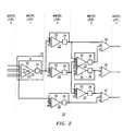
- FIGURE 1 illustrates a partial-scan, built-in, self-test circuit 10 which has been partitioned into a partial-scan chain 12, comprised of a plurality of individual flip-flops 13 coupled to form a shift register, and a near-acyclic, non-scan chain circuit portion 14, whose details are described in greater detail with respect to FIG. 2.
- the partial-scan chain 12 is similar to the scan chain described in Agrawal et al. patent No. US-A-5,043,986 and is tested by the technique of partial-scan testing as described in that patent.
- the system 10 includes a test pattern generator 16 in the form of a Linear Feedback Shift Register (LFSR) that generates a sequence of random test patterns (i.e., a plurality of successive sets of test vectors).
- the test patterns from the LSFR 16 are multiplexed by a set of multiplexers 18 with one or more primary input signals (i.e., normal operating mode signals) generated externally and intended for input to the circuit 14 (including the scan chain 12).
- the output of the multiplexer 18 is coupled to the circuit 14.
- Test patterns from the LSFR 16 are multiplexed by a second multiplexer 20 with an input signal SCANIN received by the system 10.
- the output of the multiplexer 20 is coupled to the first of the flip-flops 13 in the scan chain 12, and in response to the signal from the multiplexer, the scan chain produces an output signal SCANOUT.
- the output of the scan chain 12 is also coupled to a Multiple Input Shift Register (MISR) 22 which serves to successively compact the output signal of the scan chain with the output signal generated during a previous interval.
- MISR 20 also serves to compact output data generated by the circuit 14 with the output data generated previously by the circuit.
- the MISR 20 compacts the output signals from the scan chain 12 and from the circuit 14 to yield a bit stream referred to as a "signature" which is descriptive of the operation of the system 10. By comparing the signature of the system 10 to that for a fault-free system, the existence or absence of defects will be revealed.
- the circuit portion 14 is typically comprised of one or more sequential elements 24 (i.e., flip-flops) and one or more combinational elements 26 (i.e., gates), the elements being joined so as to create at least one node 28.
- sequential elements 24 i.e., flip-flops
- combinational elements 26 i.e., gates
- the exact nature of the elements 24 and 26 and the manner in which they are coupled is dependent on the functions to be performed by the system 10. The manner in which the elements 24 and 26 are coupled is not relevant to the invention, except that the circuit 14 has no flip-flop loops other than self-loops, as will be explained in greater detail later.
- test points may consist of either an "observation point” (i.e., a line coupled to one of the nodes 28 so as to allow the signal at the node to be observed) or a "control point” (i.e., either an AND or OR gate (not shown) interposed between the node and the signal driving it to allow the signal at the node to be controlled).
- observation point i.e., a line coupled to one of the nodes 28 so as to allow the signal at the node to be observed
- control point i.e., either an AND or OR gate (not shown) interposed between the node and the signal driving it to allow the signal at the node to be controlled.
- the circuit portion 14 is a near-acyclic circuit because it contains no flip-flop loops (i.e., the circuit portion does not contain two or more daisy-chained flip-flops 24).
- the circuit portion 14 may contain one or more self-looping flip-flops 24 which have their output coupled directly to their input and still be considered a near-acyclic circuit. (In accordance with my co-pending patent No. EP-A-0 549 130 such self-looping flip-flops would be replaced with initializable flip-flops for testing purposes.)
- the circuit portion 14 is first decomposed (modelled) in order to simplify the probabilistic calculations.
- the circuit portion 14 may be modelled by grouping the combinational elements 26 and non-self-looping flip-flips 24 into logic cones 30, which have one or more inputs and no more that one output.
- a self- looping flip-flop 24 is defined as a flip-flop which has its output coupled to its input, either directly, or through one or more gates 26).
- Each logic cone 30 whose output serves as a primary output of the circuit 14 (such as each of the logic cones located at the right-hand side of FIG. 2) is designated as a primary output block.
- a self-loop flip-flop block 32 may contain two or more overlapping logic cones 30 (i.e., the cones may share common inputs), each cone having an associated flip-flop 24. However, only one flip-flop 24 within such a block 32 may have its output coupled to the overlapping (i.e., common) inputs. Otherwise, the circuit portion 14 would no be a near-acyclic circuit.
- controllability of each node 28, representing the output of a corresponding gate 26 in FIG. 2 is determined.
- the controllability of a node 28 (expressed by the term C(28)) is defined as the probability of effecting a certain signal value at that node. For purposes of discussion, the controllability will be defined as the probability of effecting a logic "1" at a node.
- C(28) 1-C(a) where C(a) is the controllability of the input to the NOT gate.
- the controllability for a two-input NAND gate may be calculated by treating the gate as the serial combination of an AND gate and a NOT gate whose controllabilities are given by equations (1) and (3), respectively.
- the controllability of a NOR gate (not shown) may be computed in a similar fashion.
- computing the controllabilities in this fashion is an iterative process which is commenced by first calculating the controllability for each node 28 associated with each gate 26 whose input forms a primary input to the circuit 14, the primary inputs being those inputs at the left-hand edge of FIG. 2.
- the controllability computation would be commenced on those gates 26 closest to the left-hand edge of the drawing.
- the controllability at that input i.e., the probability of obtaining a prescribed logic value
- the value 0.5 indicating that it is equally likely to get a logic "1" for example as a logic "0".
- each flip-flop 24 is a more complex task than for each combinational gate 26, owing to the memory-like nature of the flip-flop.
- the task of computing the controllability of each flip-flop 24 can be simplified by modelling each non-self-loop flip-flop simply as a short-circuit between its D and Q outputs without regard to the clock input. While this approximation introduces some inaccuracy, the computation is greatly simplified.
- C(W) C(0)/(1- C(1) + C(0))
- C(0) is the controllability at the flip-flop D input after assigning a 0 controllability to the Q output and disconnecting the Q output from that of the block 32
- C(1) is the controllability at the flip-flop D input after assigning a probability of 1 at the Q flip-flop output.
- step (1) and (2) only the controllabilities of those nodes 28 of the associated logic cones 30 are computed.
- step (3) the effect of the change in the controllabilities is propagated outside the associated logic cone 30.
- each node's observability is computed.
- the observability of each node 28 (expressed by the term O(28)) is defined as the probability that a fault present at that node can be observed through one of the primary outputs of the circuit 14.
- O(28) O(output) * C(a)
- O(output) is the observability of the output of the AND gate
- C(a) is the controllability of the other AND gate input.
- the observability at the output of a NOT gate is the same as that of its input.
- Computation of the observability of each node 28 is accomplished in a manner similar to the manner in which the controllability of each node is performed, except that the observability computation is done from the primary circuit outputs (i.e., from the right-hand side of FIG. 2) to the primary circuit inputs (i.e., the left-hand side of the figure).
- SSCOM Station State Controllability Observability Measure
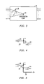
- testability of the circuit 10, and particularly, the testability of the circuit portion 14, may be enhanced by adding a test point, either in the form of an observation point 34, as seen in FIG. 3, or a control point 36, as seen in FIG. 6.
- An observation point 34 is a point at which the fault at each of a plurality of other nodes can be observed. For example in FIG. 3, the observation point 34 has been selected (in the manner described hereinafter) such that the fault at each of the nodes 28 lying in the shaded region of the circuit 14 can be observed at the observation point.
- each observation point 34 is added is straightforward. Referring to FIG. 4, which illustrates a part of the circuit portion 14, assume that a good location to observe faults is at a node 28 at the junction between a pair of gates 26. Referring to FIG. 5, to provide an observation point 34 associated with the node 28, a line 36 is provided to couple the node to the observation point 34. In practice, each observation point 34 is typically located so as to be physically accessible.
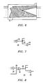
- a control point 36 is, in actuality, an element (described in greater detail with respect to FIG. 8) which serves to influence the controllability of a plurality of nodes 28 in the circuit.
- the control point 34 has been selected (in the manner described below) to influence the controllability of each of a plurality of nodes 28 lying within the cross-hatched region of the circuit 14.
- FIG. 7 which shows a part of the circuit portion 14, assume that it has been determined that the node 28, at the junction between a pair of gates 26, has been found to desirably influence the controllability of other nodes in the circuit portion 14 (not shown).
- FIG. 8 depicts the part of the circuit portion 14 shown in FIG.
- test point 36 in the form of a two-input control logic gate interposed between the gates 26, such that node 28 lies at a first input of the control logic gate and a second node 28' lies at its output.
- the control logic gate 36 of FIG. 8 serves to control the state of the signal at the node 28' in accordance with the signal at the node 28 and in accordance with the signal r at the second input of the control logic gate.
- the control logic gate 36 which forms the control point, may either take the form of an OR gate, as seen in FIG. 8, or an AND gate (not shown).
- the particular structure of the gate 36 depends on the controllability of the node 28. If the controllability of the node 28, as calculated by the SSCOM technique discussed previously, is less than a prescribed value (i.e., ⁇ 0.5), the gate 36 takes the form of an OR gate. On the other hand, if the controllability at the node 28' is above a prescribed value (i.e., > 0.5), the gate 36 is chosen as an AND gate.
- test points each taking the form of either an observation point 34 and/or a control point 36
- the following method is employed to select test points to achieve a desired level of fault coverage during testing of the circuit 14 by the application of t random patterns generated by the test pattern generator 16 of FIG. 1 with the minimum number of test points:
- the first procedure is intended to better detect hard-to- control faults by the addition of one or more control points 36.
- the second procedure is intended to detect hard-to-observe faults by the addition of one or more observation points 34.
- the rationale for adding control points 36 prior to the addition of observation points 34 is that the addition of a control point may in fact increase the observability of one or more nodes without the need to add an observation point 34.
- the control points 36 are added in ascending level-vector order, the number of such points required is reduced because the insertion of a control point can improve not only the controllability of a given node, but the nodes which are in its fanout cone as well. Note that the observability of a node 28 can be improved by inserting either an observation point 34 or a control point 36.
- the foregoing discloses a technique for improving the testability of a near-acyclic circuit 14 by the selective addition of at least one test point, either in the form of a control point 36 and/or an observation point 34 to increase the level of fault coverage.
Landscapes
- Engineering & Computer Science (AREA)
- General Engineering & Computer Science (AREA)
- Physics & Mathematics (AREA)
- General Physics & Mathematics (AREA)
- Tests Of Electronic Circuits (AREA)
- Test And Diagnosis Of Digital Computers (AREA)
Applications Claiming Priority (2)
| Application Number | Priority Date | Filing Date | Title |
|---|---|---|---|
| US08/063,191 US5450414A (en) | 1993-05-17 | 1993-05-17 | Partial-scan built-in self-testing circuit having improved testability |
| US63191 | 1993-05-17 |
Publications (2)
| Publication Number | Publication Date |
|---|---|
| EP0631235A1 EP0631235A1 (en) | 1994-12-28 |
| EP0631235B1 true EP0631235B1 (en) | 1998-08-12 |
Family
ID=22047570
Family Applications (1)
| Application Number | Title | Priority Date | Filing Date |
|---|---|---|---|
| EP94303226A Expired - Lifetime EP0631235B1 (en) | 1993-05-17 | 1994-05-04 | Partial-scan built-in selftesting sequential circuit |
Country Status (6)
| Country | Link |
|---|---|
| US (1) | US5450414A (Sortimente) |
| EP (1) | EP0631235B1 (Sortimente) |
| JP (1) | JP3048500B2 (Sortimente) |
| KR (1) | KR0163968B1 (Sortimente) |
| CA (1) | CA2119226C (Sortimente) |
| TW (1) | TW245776B (Sortimente) |
Families Citing this family (54)
| Publication number | Priority date | Publication date | Assignee | Title |
|---|---|---|---|---|
| US5748497A (en) * | 1994-10-31 | 1998-05-05 | Texas Instruments Incorporated | System and method for improving fault coverage of an electric circuit |
| US5831992A (en) * | 1995-08-17 | 1998-11-03 | Northern Telecom Limited | Methods and apparatus for fault diagnosis in self-testable systems |
| CA2187466A1 (en) * | 1995-10-19 | 1997-04-20 | Kwang-Ting Cheng | Method for inserting test points for full- and partial-scan built-in self-testing |
| US5668816A (en) * | 1996-08-19 | 1997-09-16 | International Business Machines Corporation | Method and apparatus for injecting errors into an array built-in self-test |
| KR100206128B1 (ko) * | 1996-10-21 | 1999-07-01 | 윤종용 | 선형 궤환 쉬프트레지스터, 다중 입력기호 레지스터 및 이들을 이용한 내장 자기 진단회로 |
| US5691990A (en) * | 1996-12-02 | 1997-11-25 | International Business Machines Corporation | Hybrid partial scan method |
| KR100499818B1 (ko) * | 1997-01-06 | 2005-11-22 | 가부시끼가이샤 히다치 세이사꾸쇼 | 반도체집적회로검사점의해석방법,해석장치 |
| JP2000513815A (ja) * | 1997-04-24 | 2000-10-17 | コーニンクレッカ フィリップス エレクトロニクス エヌ ヴィ | ディジタル回路を走査試験可能にする方法 |
| WO1998049576A1 (fr) * | 1997-04-25 | 1998-11-05 | Hitachi, Ltd. | Circuit logique et son procede d'essai |
| US6256759B1 (en) | 1998-06-15 | 2001-07-03 | Agere Systems Inc. | Hybrid algorithm for test point selection for scan-based BIST |
| US6363520B1 (en) | 1998-06-16 | 2002-03-26 | Logicvision, Inc. | Method for testability analysis and test point insertion at the RT-level of a hardware development language (HDL) specification |
| SE512916C2 (sv) | 1998-07-16 | 2000-06-05 | Ericsson Telefon Ab L M | Metod och anordning för feldetektering i digitalt system |
| US7036060B2 (en) | 1998-09-22 | 2006-04-25 | Hitachi, Ltd. | Semiconductor integrated circuit and its analyzing method |
| US6370664B1 (en) | 1998-10-29 | 2002-04-09 | Agere Systems Guardian Corp. | Method and apparatus for partitioning long scan chains in scan based BIST architecture |
| US6301688B1 (en) * | 1998-11-24 | 2001-10-09 | Agere Systems Optoelectronics Guardian Corp. | Insertion of test points in RTL designs |
| US7281185B2 (en) * | 1999-06-08 | 2007-10-09 | Cadence Design (Israel) Ii Ltd. | Method and apparatus for maximizing and managing test coverage |
| US7114111B2 (en) * | 1999-06-08 | 2006-09-26 | Cadence Design (Isreal) Ii Ltd. | Method and apparatus for maximizing test coverage |
| US6578167B2 (en) | 1999-08-06 | 2003-06-10 | Hewlett-Packard Development Company, L.P. | Digital Component test Apparatus, an apparatus for testing electronic assemblies and a method for remotely testing a peripheral device having an electronic assembly |
| US6463561B1 (en) | 1999-09-29 | 2002-10-08 | Agere Systems Guardian Corp. | Almost full-scan BIST method and system having higher fault coverage and shorter test application time |
| US6694466B1 (en) * | 1999-10-27 | 2004-02-17 | Agere Systems Inc. | Method and system for improving the test quality for scan-based BIST using a general test application scheme |
| US7493540B1 (en) | 1999-11-23 | 2009-02-17 | Jansuz Rajski | Continuous application and decompression of test patterns to a circuit-under-test |
| US6327687B1 (en) * | 1999-11-23 | 2001-12-04 | Janusz Rajski | Test pattern compression for an integrated circuit test environment |
| US9134370B2 (en) | 1999-11-23 | 2015-09-15 | Mentor Graphics Corporation | Continuous application and decompression of test patterns and selective compaction of test responses |
| US9664739B2 (en) | 1999-11-23 | 2017-05-30 | Mentor Graphics Corporation | Continuous application and decompression of test patterns and selective compaction of test responses |
| US6684358B1 (en) | 1999-11-23 | 2004-01-27 | Janusz Rajski | Decompressor/PRPG for applying pseudo-random and deterministic test patterns |
| EP1242885B1 (en) * | 1999-11-23 | 2009-10-07 | Mentor Graphics Corporation | Continuous application and decompression of test patterns to a circuit-under-test |
| US6557129B1 (en) | 1999-11-23 | 2003-04-29 | Janusz Rajski | Method and apparatus for selectively compacting test responses |
| US6353842B1 (en) | 1999-11-23 | 2002-03-05 | Janusz Rajski | Method for synthesizing linear finite state machines |
| US8533547B2 (en) | 1999-11-23 | 2013-09-10 | Mentor Graphics Corporation | Continuous application and decompression of test patterns and selective compaction of test responses |
| US6874109B1 (en) | 1999-11-23 | 2005-03-29 | Janusz Rajski | Phase shifter with reduced linear dependency |
| US6745373B2 (en) * | 2001-02-20 | 2004-06-01 | International Business Machines Corporation | Method for insertion of test points into integrated circuit logic designs |
| WO2004027440A1 (ja) * | 2002-09-19 | 2004-04-01 | Fujitsu Limited | 集積回路試験装置および試験方法 |
| US7299391B2 (en) * | 2002-10-29 | 2007-11-20 | Faraday Technology Corp. | Circuit for control and observation of a scan chain |
| US7302624B2 (en) * | 2003-02-13 | 2007-11-27 | Janusz Rajski | Adaptive fault diagnosis of compressed test responses |
| EP1595211B1 (en) | 2003-02-13 | 2008-07-09 | Mentor Graphics Corporation | Compressing test responses using a compactor |
| US7437640B2 (en) * | 2003-02-13 | 2008-10-14 | Janusz Rajski | Fault diagnosis of compressed test responses having one or more unknown states |
| US7509550B2 (en) * | 2003-02-13 | 2009-03-24 | Janusz Rajski | Fault diagnosis of compressed test responses |
| JP2005135226A (ja) * | 2003-10-31 | 2005-05-26 | Matsushita Electric Ind Co Ltd | 半導体集積回路のテスト回路挿入方法及び装置 |
| SG126774A1 (en) * | 2005-04-06 | 2006-11-29 | Agilent Technologies Inc | Method for determining a set of guard points and asystem for use thereof |
| US7493434B1 (en) * | 2005-05-25 | 2009-02-17 | Dafca, Inc. | Determining the value of internal signals in a malfunctioning integrated circuit |
| JP5136043B2 (ja) * | 2007-02-22 | 2013-02-06 | 富士通セミコンダクター株式会社 | 論理回路および記録媒体 |
| JP2008293088A (ja) | 2007-05-22 | 2008-12-04 | Nec Electronics Corp | 半導体集積回路及びその設計方法 |
| US7882454B2 (en) * | 2008-04-28 | 2011-02-01 | International Business Machines Corporation | Apparatus and method for improved test controllability and observability of random resistant logic |
| US8164345B2 (en) * | 2008-05-16 | 2012-04-24 | Rutgers, The State University Of New Jersey | Spectral and information theoretic method of test point, partial-scan, and full-scan flip-flop insertion to improve integrated circuit testability |
| JP2011112434A (ja) * | 2009-11-25 | 2011-06-09 | Renesas Electronics Corp | 論理回路用テストポイント挿入方法、論理回路試験装置 |
| US8819507B2 (en) * | 2010-05-10 | 2014-08-26 | Raytheon Company | Field programmable gate arrays with built-in self test mechanisms |
| US8887109B1 (en) * | 2013-05-17 | 2014-11-11 | Synopsys, Inc. | Sequential logic sensitization from structural description |
| EP3105674B1 (en) | 2013-11-28 | 2018-01-10 | Telefonaktiebolaget LM Ericsson (publ) | Testing a feedback shift-register |
| US10372855B2 (en) * | 2014-02-28 | 2019-08-06 | Mentor Graphics Corporation | Scan cell selection for partial scan designs |
| US10527674B2 (en) | 2017-08-21 | 2020-01-07 | International Business Machines Corporation | Circuit structures to resolve random testability |
| KR102450484B1 (ko) * | 2020-12-18 | 2022-09-30 | 연세대학교 산학협력단 | 테스트 포인트 삽입을 통하여 향상된 검출율을 가지는 고장 검출 방법, 고장 검출 장치 및 가중치 인가 회로 |
| KR102513278B1 (ko) * | 2021-04-16 | 2023-03-23 | 연세대학교 산학협력단 | 스캔 체인의 자가 테스트를 위한 삽입 노드 결정 방법 및 장치 |
| KR102680120B1 (ko) * | 2021-11-29 | 2024-06-28 | 연세대학교 산학협력단 | 컨트롤 포인트의 구동 제어 방법 및 장치 |
| US12130330B2 (en) * | 2023-01-25 | 2024-10-29 | Qualcomm Incorporated | Integrated circuit including constant-0 flip flops reconfigured to provide observable and controllable test points |
Family Cites Families (8)
| Publication number | Priority date | Publication date | Assignee | Title |
|---|---|---|---|---|
| US4225957A (en) * | 1978-10-16 | 1980-09-30 | International Business Machines Corporation | Testing macros embedded in LSI chips |
| GB2049958B (en) * | 1979-03-15 | 1983-11-30 | Nippon Electric Co | Integrated logic circuit adapted to performance tests |
| US4534028A (en) * | 1983-12-01 | 1985-08-06 | Siemens Corporate Research & Support, Inc. | Random testing using scan path technique |
| US5103557A (en) * | 1988-05-16 | 1992-04-14 | Leedy Glenn J | Making and testing an integrated circuit using high density probe points |
| US5043986A (en) * | 1989-05-18 | 1991-08-27 | At&T Bell Laboratories | Method and integrated circuit adapted for partial scan testability |
| US5132974A (en) * | 1989-10-24 | 1992-07-21 | Silc Technologies, Inc. | Method and apparatus for designing integrated circuits for testability |
| JPH03201035A (ja) * | 1989-10-24 | 1991-09-02 | Matsushita Electric Ind Co Ltd | 検査系列生成方法 |
| US5291495A (en) * | 1991-07-12 | 1994-03-01 | Ncr Corporation | Method for designing a scan path for a logic circuit and testing of the same |
-
1993
- 1993-05-17 US US08/063,191 patent/US5450414A/en not_active Expired - Lifetime
-
1994
- 1994-03-16 TW TW083102304A patent/TW245776B/zh active
- 1994-03-16 CA CA002119226A patent/CA2119226C/en not_active Expired - Fee Related
- 1994-05-04 EP EP94303226A patent/EP0631235B1/en not_active Expired - Lifetime
- 1994-05-16 KR KR1019940010613A patent/KR0163968B1/ko not_active Expired - Fee Related
- 1994-05-16 JP JP6124713A patent/JP3048500B2/ja not_active Expired - Lifetime
Also Published As
| Publication number | Publication date |
|---|---|
| CA2119226C (en) | 1998-08-04 |
| TW245776B (Sortimente) | 1995-04-21 |
| US5450414A (en) | 1995-09-12 |
| CA2119226A1 (en) | 1994-11-18 |
| KR0163968B1 (ko) | 1999-03-20 |
| EP0631235A1 (en) | 1994-12-28 |
| JPH06331709A (ja) | 1994-12-02 |
| JP3048500B2 (ja) | 2000-06-05 |
Similar Documents
| Publication | Publication Date | Title |
|---|---|---|
| EP0631235B1 (en) | Partial-scan built-in selftesting sequential circuit | |
| Edirisooriya et al. | Diagnosis of scan path failures | |
| Krstic et al. | Delay fault testing for VLSI circuits | |
| EP1722246B1 (en) | Method and apparatus for selectively compacting test responses | |
| US6993694B1 (en) | Deterministic bist architecture including MISR filter | |
| Iyengar et al. | Synthesis of pseudo-random pattern testable designs | |
| US10747926B2 (en) | Low-power test compression for launch-on-capture transition fault testing | |
| US6256759B1 (en) | Hybrid algorithm for test point selection for scan-based BIST | |
| US7266746B2 (en) | Device and method for testing integrated circuit | |
| IE56976B1 (en) | Improvements in or relating to integrated circuits | |
| Chen et al. | A methodology to design efficient BIST test pattern generators | |
| JPH1049567A (ja) | 回路設計の可試験性を向上させる方法 | |
| US7610527B2 (en) | Test output compaction with improved blocking of unknown values | |
| US6484294B1 (en) | Semiconductor integrated circuit and method of designing the same | |
| US5828828A (en) | Method for inserting test points for full-and-partial-scan built-in self-testing | |
| JPH04236378A (ja) | 論理装置を試験する方法および装置 | |
| US6728917B2 (en) | Sequential test pattern generation using combinational techniques | |
| US7299394B2 (en) | Method and apparatus for determining optimum initial value for test pattern generator | |
| Rudnick et al. | An observability enhancement approach for improved testability and at-speed test | |
| Cho et al. | Test application time reduction for scan circuits using limited scan operations | |
| HK1097600B (en) | Method and apparatus for selectively compacting test responses | |
| JPH10197602A (ja) | 半導体集積回路 |
Legal Events
| Date | Code | Title | Description |
|---|---|---|---|
| PUAI | Public reference made under article 153(3) epc to a published international application that has entered the european phase |
Free format text: ORIGINAL CODE: 0009012 |
|
| AK | Designated contracting states |
Kind code of ref document: A1 Designated state(s): FR GB IT NL |
|
| 17P | Request for examination filed |
Effective date: 19950615 |
|
| 17Q | First examination report despatched |
Effective date: 19961018 |
|
| GRAG | Despatch of communication of intention to grant |
Free format text: ORIGINAL CODE: EPIDOS AGRA |
|
| GRAG | Despatch of communication of intention to grant |
Free format text: ORIGINAL CODE: EPIDOS AGRA |
|
| GRAH | Despatch of communication of intention to grant a patent |
Free format text: ORIGINAL CODE: EPIDOS IGRA |
|
| GRAH | Despatch of communication of intention to grant a patent |
Free format text: ORIGINAL CODE: EPIDOS IGRA |
|
| GRAA | (expected) grant |
Free format text: ORIGINAL CODE: 0009210 |
|
| AK | Designated contracting states |
Kind code of ref document: B1 Designated state(s): FR GB IT NL |
|
| ITF | It: translation for a ep patent filed | ||
| ET | Fr: translation filed | ||
| PLBE | No opposition filed within time limit |
Free format text: ORIGINAL CODE: 0009261 |
|
| STAA | Information on the status of an ep patent application or granted ep patent |
Free format text: STATUS: NO OPPOSITION FILED WITHIN TIME LIMIT |
|
| 26N | No opposition filed | ||
| PGFP | Annual fee paid to national office [announced via postgrant information from national office to epo] |
Ref country code: GB Payment date: 20010426 Year of fee payment: 8 |
|
| PGFP | Annual fee paid to national office [announced via postgrant information from national office to epo] |
Ref country code: NL Payment date: 20010427 Year of fee payment: 8 |
|
| PGFP | Annual fee paid to national office [announced via postgrant information from national office to epo] |
Ref country code: FR Payment date: 20010502 Year of fee payment: 8 |
|
| REG | Reference to a national code |
Ref country code: GB Ref legal event code: IF02 |
|
| PG25 | Lapsed in a contracting state [announced via postgrant information from national office to epo] |
Ref country code: GB Free format text: LAPSE BECAUSE OF NON-PAYMENT OF DUE FEES Effective date: 20020504 |
|
| PG25 | Lapsed in a contracting state [announced via postgrant information from national office to epo] |
Ref country code: NL Free format text: LAPSE BECAUSE OF NON-PAYMENT OF DUE FEES Effective date: 20021201 |
|
| GBPC | Gb: european patent ceased through non-payment of renewal fee |
Effective date: 20020504 |
|
| PG25 | Lapsed in a contracting state [announced via postgrant information from national office to epo] |
Ref country code: FR Free format text: LAPSE BECAUSE OF NON-PAYMENT OF DUE FEES Effective date: 20030131 |
|
| NLV4 | Nl: lapsed or anulled due to non-payment of the annual fee |
Effective date: 20021201 |
|
| REG | Reference to a national code |
Ref country code: FR Ref legal event code: ST |
|
| PG25 | Lapsed in a contracting state [announced via postgrant information from national office to epo] |
Ref country code: IT Free format text: LAPSE BECAUSE OF NON-PAYMENT OF DUE FEES Effective date: 20050504 |