EP0623955A2 - Halbleiterchipmodul - Google Patents
Halbleiterchipmodul Download PDFInfo
- Publication number
- EP0623955A2 EP0623955A2 EP94303149A EP94303149A EP0623955A2 EP 0623955 A2 EP0623955 A2 EP 0623955A2 EP 94303149 A EP94303149 A EP 94303149A EP 94303149 A EP94303149 A EP 94303149A EP 0623955 A2 EP0623955 A2 EP 0623955A2
- Authority
- EP
- European Patent Office
- Prior art keywords
- semiconductor chip
- semiconductor
- semiconductor substrate
- chip module
- substrate
- Prior art date
- Legal status (The legal status is an assumption and is not a legal conclusion. Google has not performed a legal analysis and makes no representation as to the accuracy of the status listed.)
- Withdrawn
Links
Images

Classifications
-
- H10W72/00—
-
- H10W70/413—
-
- H10W72/073—
-
- H10W72/07331—
-
- H10W72/07337—
-
- H10W72/354—
-
- H10W74/00—
-
- H10W90/756—
Definitions
- This invention relates, in general, to semiconductor chips, and more particularly, but not limited to, a semiconductor chip module used in a semiconductor package.
- interconnection system Semiconductor chips or integrated circuits are typically bonded to an external, electrical interconnection system (hereinafter interconnection system).
- the interconnection system enables one to electrically connect the semiconductor chip to an external system.
- This interconnection typically includes a metal leads or a leadframe having an integral or a separate metal heatsink.
- the semiconductor chip is electrically connected to the leads.
- the chip and a portion of the interconnection system are typically encapsulated or housed in a metal or ceramic housing.
- the interconnection system as used herein, also describes chips bonded to a printed circuit board.
- a silicon chip or die with or without metal deposited on the back side is attached to the metal leadframe or a metal heatsink through a die attach or adhesive media.
- the die attach or adhesive media is comprised of solder or other metallic materials, or an epoxy based material.
- a thermal mismatch occurs between the semiconductor material of the semiconductor chip and the die attach material, and the die attach material and the metallic leadframe. Problems with these interconnection systems include die cracking due to thermal mismatch, failure of the bond between the die and the die attach material, and voiding in conventional solder and epoxy die attach systems.
- a semiconductor chip module is formed by providing at least one semiconductor chip and a semiconductor substrate and bonding the semiconductor chip to the semiconductor substrate without the use of an epoxy or a metallic layer to create a bond between the semiconductor chip and the semiconductor substrate.
- the semiconductor chip may be electrically connected to an external, electrical interconnection system.
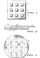
- FIG. 1 illustrates a top view of an embodiment of the present invention in a beginning stage of processing
- FIG. 2 illustrates a cross-sectional view of an embodiment of the present invention in a further stage of processing
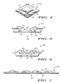
- FIG. 3 illustrates a top view of an embodiment of the present invention in a further stage of processing
- FIG. 4 illustrates a perspective view of an embodiment of the present further along in processing
- FIG. 5 illustrates a side view of the structure of
- FIG. 4 further along in process in a first embodiment of the present invention
- FIG. 6 illustrates a side view of the structure of
- FIG. 4 further along in process in a second embodiment of the present invention.
- FIG. 7 illustrates a side view of the structure of
- FIG. 4 further along in process in a third embodiment of the present invention.
- FIG. 8 illustrates a flow chart of an embodiment of a process flow of the present invention.
- FIG. 1 illustrates a top view of a beginning process of forming a semiconductor chip module for final assembly into a package.
- FIG. 8 illustrates a flowchart of the present invention.
- a holder or carrier 10 having a plurality of spaced slots 12 in which a plurality of semiconductor chips 20 are placed.
- This type of holder 10 is typically called a waffle pack, with this one having a stretch grid in which semiconductor chips 20 are spaced apart from each other by a particular distance.
- Semiconductor chips 20 can be placed into holder 10 by using a pick and place method.
- the plurality of semiconductor chips 20 are placed front side 21 (shown in FIG. 4) up in holder 10.
- FIG. 2 illustrates the plurality of semiconductor chips 20 picked up by a vacuum frame 15 from holder 10.
- Vacuum frame 15 is comprised of a multi-port pick-up surface with a vacuum 17 attached thereto. Vacuum 17 is connected to conduits 18.
- back side 22 shown in FIG. 4
- the plurality of semiconductor chips 20 are held in place by vacuum pickup 15 it is submerged in a cleaning solution, preferably an ammonia-hydrogen peroxide solution, for an appropriate amount of time necessary to clean the surface.
- a cleaning solution preferably an ammonia-hydrogen peroxide solution
- semiconductor substrate 30 is then provided.
- semiconductor substrate 30 is a wafer of the size which is typically used to form a plurality of semiconductor chips 20 thereon. For example, a 4, 5, 6, or even a 12 inch wafer is used in the art. Also, semiconductor substrate 30 is similarly cleaned.
- Backside 22 of semiconductor chips 20 are joined to front side 31 (shown in FIG. 4) of semiconductor substrate 30.
- semiconductor substrate 30 and the plurality of semiconductor chips 20 are placed in a horizontal position in a furnace preferably having a temperature of approximately 200 to 400°C for at least approximately one hour. Bonding may also take place in a vertical position, with a small force applied to semiconductor chips 20 and semiconductor substrate 30. Note that in conventional wafer-to-wafer bonding, rather than chip-to-wafer bonding as done here, a much higher temperature must be used. The temperature range and time chosen is believed to produce an optimum bond between each semiconductor chip 20 and semiconductor substrate 30.
- semiconductor chip 20 is bonded to a portion of semiconductor substrate 30 without the use of an adhesive media (epoxy) or a metallic layer. This is important because an adhesive media or metallic layer has a substantially different thermal coefficient of expansion than semiconductor chip 20 or semiconductor substrate 30.
- semiconductor substrate 30 is comprised of a semiconductor material which is used to form semiconductor chip 20. Even if semiconductor substrate 30 and semiconductor chip 20 are comprised of dissimilar semiconductor materials, the thermal properties are closer than the thermal properties of a semiconductor material and a metal or an epoxy.
- either the front side 31 of semiconductor substrate 30 or backside of semiconductor chip 20 has an oxidized layer chemically formed thereon to minimize or prevent the formation of voids.
- this oxidized layer is thermally grown on semiconductor substrate 30 or semiconductor chip 20 by oxidizing the semiconductor material of semiconductor chip 20 or semiconductor substrate 30. If the semiconductor material is comprised of silicon, then preferably the oxidized layer is comprised of silicon dioxide. Note that one element of the oxidized layer is comprised of the semiconductor material. The thickness of the oxidized layer is thin enough that it is negligible in terms of causing problems with semiconductor substrate 30 and semiconductor chip 20 having matched thermal properties. In other words, the oxidized layer does not introduce a significant thermal mismatch to the semiconductor chip module 35 of the present invention. Thus, the present invention avoids the host of failure mechanisms associated with interconnections systems having thermal mismatch.
- FIG. 3 illustrates a top view of semiconductor substrate 30 in the process of singulating at least one semiconductor chip 20 into a module 35 (shown in FIG. 4). Dashed lines 40 indicate where semiconductor substrate 30 may be sawn into a plurality of modules 35. Other methods of singulating semiconductor substrate 30 may be used.
- FIG. 4 illustrates a single semiconductor chip module 35 having a front side 31 and a back side 32.
- a single semiconductor chip 20 having a front side 21 and a back side 22 is bonded to a portion of semiconductor substrate 30.
- the portion of semiconductor substrate 30 is larger than semiconductor chip(s) 20 bonded thereon.
- FIG. 5 illustrates a semiconductor chip module 35 bonded to an interconnection system 49. Electrical connection 54 is made between leads 51 and semiconductor chip 20.
- metal heatsink 50 is separate from leads 51.
- FIG. 5 illustrates only one way in which semiconductor chip module 35 may be attached to metal heatsink 50.
- semiconductor chip module 35 is attached to metal heatsink 50 by attaching front side 31 of semiconductor chip module 35 to metal heatsink 50 by using a thermally conductive bonding material 52, such an electrically conductive or nonconductive epoxy or a solder in this embodiment.
- the portion of semiconductor substrate 30 replaces a portion of a conventional metal heatsink.
- metal heatsink 50 is provided with an opening so that semiconductor chip 20 is exposed on the front side.
- metal heatsink 50 has a step or notch 53 to which semiconductor substrate 30 is bonded to metal heatsink 50.
- This step 53 is not necessary for all packages, but provides for a coplanar surface when thermally required. This coplanar surface improves the thermal performance characteristics of interconnection system 49.
- a plastic encapsulant or other housing may then be formed to house semiconductor chip module 35, heatsink 50 and a portion of leads 51.
- FIG. 6 illustrates an interconnection system 60, another embodiment of the present invention.
- front side 31 of semiconductor chip module 35 can be attached to the leads or leadframe 56 through bonding material 52 as described above with reference to FIG. 5.
- Electrical connection 54 may be made between leads 56 and semiconductor chip 20 if bonding material 52 is electrically nonconductive.
- a plastic encapsulant 65 may be formed to encapsulate semiconductor chip module 35 and a portion of leads 56. Many processes are known in the art to accomplish this packaging step. In this embodiment, the portion of semiconductor substrate 30 replaces the metal heatsink of the prior art.
- thermal mismatch between semiconductor chip module 35 and metal heatsink 50 (FIG. 5) or leadframe 56 (FIG. 6)
- the thermal mismatch between the chip 20 and the material adjacent chip 20 is removed.
- area in which there is thermal mismatch is smaller than in the prior art because only a portion of semiconductor substrate 30 is bonded to the metal heatsink or leads.
- the material adjacent the chip was a solder or epoxy layer and then the metal heatsink adjacent to that.
- FIG. 7 illustrates yet another embodiment of the present invention.
- semiconductor chip module 35 is used to replace all or a portion of a board in a printed circuit board.
- Electrically isolated metal layers or stripes 72 (which act as leads) can be formed directly on a portion of substrate 30.
- Metal layer 72 are electrically isolated from each other and the portion of semiconductor substrate 30.
- One way of forming isolated metal layers 72 is by forming an insulating layer on front side 31 of semiconductor substrate 30 and subsequently forming a metal layer (through evaporation or sputtering) on the insulating layer. The metal layer and insulating layer are then patterned to form a plurality of isolated metal layers 72 and an insulating portion (or a plurality of insulating portions) 74.
- FIG. 8 illustrates a flow chart of the process used in the present invention to fabricate a semiconductor chip module.
- the die does not have to be bonded directly to a metallic heatsink through an adhesive media thus thermal mismatch is prevented.
- Thermal mismatch leads to high stresses in the adhesive media and has been known to cause die cracking.
- the thermal performance of the interconnection system is enhanced by the elimination of thermal mismatch.
Landscapes
- Cooling Or The Like Of Semiconductors Or Solid State Devices (AREA)
- Die Bonding (AREA)
Applications Claiming Priority (2)
| Application Number | Priority Date | Filing Date | Title |
|---|---|---|---|
| US08/055,888 US5473192A (en) | 1993-05-04 | 1993-05-04 | Unitary silicon die module |
| US55888 | 1993-05-04 |
Publications (2)
| Publication Number | Publication Date |
|---|---|
| EP0623955A2 true EP0623955A2 (de) | 1994-11-09 |
| EP0623955A3 EP0623955A3 (de) | 1995-04-26 |
Family
ID=22000824
Family Applications (1)
| Application Number | Title | Priority Date | Filing Date |
|---|---|---|---|
| EP94303149A Withdrawn EP0623955A3 (de) | 1993-05-04 | 1994-04-29 | Halbleiterchipmodul. |
Country Status (5)
| Country | Link |
|---|---|
| US (1) | US5473192A (de) |
| EP (1) | EP0623955A3 (de) |
| JP (1) | JPH06333962A (de) |
| KR (1) | KR940027146A (de) |
| CN (1) | CN1095862A (de) |
Cited By (2)
| Publication number | Priority date | Publication date | Assignee | Title |
|---|---|---|---|---|
| WO2002060811A3 (en) * | 2001-01-30 | 2003-03-20 | Axsun Tech Inc | Mems singulation process utilizing protective coating |
| CN102412226A (zh) * | 2010-09-17 | 2012-04-11 | 安森美半导体贸易公司 | 半导体装置 |
Families Citing this family (6)
| Publication number | Priority date | Publication date | Assignee | Title |
|---|---|---|---|---|
| US6261867B1 (en) | 1998-03-13 | 2001-07-17 | Stratedge Corporation | Method of making a package for microelectronic devices using iron oxide as a bonding agent |
| US6534851B1 (en) * | 2000-08-21 | 2003-03-18 | Agere Systems, Inc. | Modular semiconductor substrates |
| KR100621617B1 (ko) * | 2003-08-27 | 2006-09-13 | 삼성전자주식회사 | 메모리 모듈 구조 |
| JP2006082260A (ja) * | 2004-09-14 | 2006-03-30 | Oki Data Corp | 半導体複合装置、半導体複合装置の製造方法、半導体複合装置を使用したledヘッド及びこのledヘッドを用いた画像形成装置 |
| US7238589B2 (en) * | 2004-11-01 | 2007-07-03 | International Business Machines Corporation | In-place bonding of microstructures |
| JP5467579B2 (ja) | 2010-06-01 | 2014-04-09 | 株式会社沖データ | 半導体複合装置の製造方法 |
Family Cites Families (7)
| Publication number | Priority date | Publication date | Assignee | Title |
|---|---|---|---|---|
| DE3583183D1 (de) * | 1984-05-09 | 1991-07-18 | Toshiba Kawasaki Kk | Verfahren zur herstellung eines halbleitersubstrates. |
| US4818323A (en) * | 1987-06-26 | 1989-04-04 | Motorola Inc. | Method of making a void free wafer via vacuum lamination |
| JPH0752738B2 (ja) * | 1987-09-18 | 1995-06-05 | 日本電気株式会社 | 半導体素子のマウント方法 |
| US5010036A (en) * | 1990-04-20 | 1991-04-23 | Eaton Corporation | Low temperature semiconductor bonding process with chemical vapor reaction |
| GB9014491D0 (en) * | 1990-06-29 | 1990-08-22 | Digital Equipment Int | Mounting silicon chips |
| US5175613A (en) * | 1991-01-18 | 1992-12-29 | Digital Equipment Corporation | Package for EMI, ESD, thermal, and mechanical shock protection of circuit chips |
| US5198963A (en) * | 1991-11-21 | 1993-03-30 | Motorola, Inc. | Multiple integrated circuit module which simplifies handling and testing |
-
1993
- 1993-05-04 US US08/055,888 patent/US5473192A/en not_active Expired - Fee Related
-
1994
- 1994-04-25 KR KR1019940008685A patent/KR940027146A/ko not_active Ceased
- 1994-04-27 JP JP6110210A patent/JPH06333962A/ja active Pending
- 1994-04-29 EP EP94303149A patent/EP0623955A3/de not_active Withdrawn
- 1994-04-29 CN CN94105000A patent/CN1095862A/zh active Pending
Cited By (3)
| Publication number | Priority date | Publication date | Assignee | Title |
|---|---|---|---|---|
| WO2002060811A3 (en) * | 2001-01-30 | 2003-03-20 | Axsun Tech Inc | Mems singulation process utilizing protective coating |
| CN102412226A (zh) * | 2010-09-17 | 2012-04-11 | 安森美半导体贸易公司 | 半导体装置 |
| CN102412226B (zh) * | 2010-09-17 | 2015-04-01 | 半导体元件工业有限责任公司 | 半导体装置 |
Also Published As
| Publication number | Publication date |
|---|---|
| CN1095862A (zh) | 1994-11-30 |
| KR940027146A (ko) | 1994-12-10 |
| JPH06333962A (ja) | 1994-12-02 |
| EP0623955A3 (de) | 1995-04-26 |
| US5473192A (en) | 1995-12-05 |
Similar Documents
| Publication | Publication Date | Title |
|---|---|---|
| US6218728B1 (en) | Mold-BGA-type semiconductor device and method for making the same | |
| US5703405A (en) | Integrated circuit chip formed from processing two opposing surfaces of a wafer | |
| US5726500A (en) | Semiconductor hybrid component | |
| US5273940A (en) | Multiple chip package with thinned semiconductor chips | |
| US4525921A (en) | High-density electronic processing package-structure and fabrication | |
| US20050042786A1 (en) | Process for making contact with and housing integrated circuits | |
| US6822336B2 (en) | Semiconductor device | |
| US7473581B2 (en) | Wafer stacking package method | |
| KR20010004562A (ko) | 칩 사이즈 스택 패키지 및 그의 제조 방법 | |
| EP2087516A2 (de) | Herstellung von chips mit deckeln auf waferebene mit elektroabgeschiedener dielektrischer beschichtung | |
| CN1153997A (zh) | 改进的减小尺寸的集成芯片封装 | |
| US20120217657A1 (en) | Multi-chip module package | |
| US5473192A (en) | Unitary silicon die module | |
| FR2645681A1 (fr) | Dispositif d'interconnexion verticale de pastilles de circuits integres et son procede de fabrication | |
| US3986251A (en) | Germanium doped light emitting diode bonding process | |
| JP2005294443A (ja) | 半導体装置及びその製造方法 | |
| US8324115B2 (en) | Semiconductor chip, semiconductor device and methods for producing the same | |
| US4530001A (en) | High voltage integrated semiconductor devices using a thermoplastic resin layer | |
| US5959352A (en) | Chip arrangement and method of producing the same | |
| CN101305464A (zh) | 芯片组件和制造芯片组件的方法 | |
| EP0525651B1 (de) | Packungsstruktur für integrierte Schaltungschips | |
| JP2529087B2 (ja) | 熱整合されたicチップ装置の製造方法 | |
| EP0032565B1 (de) | Verfahren zur Montierung und Kapselung von Halbleiteranordnungen auf keramischen Substraten und eingekapselte Halbleiteranordnungen | |
| US20050082658A1 (en) | Simplified stacked chip assemblies | |
| US5512780A (en) | Inorganic chip-to-package interconnection circuit |
Legal Events
| Date | Code | Title | Description |
|---|---|---|---|
| PUAI | Public reference made under article 153(3) epc to a published international application that has entered the european phase |
Free format text: ORIGINAL CODE: 0009012 |
|
| AK | Designated contracting states |
Kind code of ref document: A2 Designated state(s): DE FR GB IT |
|
| PUAL | Search report despatched |
Free format text: ORIGINAL CODE: 0009013 |
|
| AK | Designated contracting states |
Kind code of ref document: A3 Designated state(s): DE FR GB IT |
|
| 17P | Request for examination filed |
Effective date: 19951026 |
|
| 17Q | First examination report despatched |
Effective date: 19971110 |
|
| STAA | Information on the status of an ep patent application or granted ep patent |
Free format text: STATUS: THE APPLICATION IS DEEMED TO BE WITHDRAWN |
|
| 18D | Application deemed to be withdrawn |
Effective date: 19990605 |