EP0614321A2 - Farbanzeigevorrichtung mit Plasmaanzeigetafel - Google Patents
Farbanzeigevorrichtung mit Plasmaanzeigetafel Download PDFInfo
- Publication number
- EP0614321A2 EP0614321A2 EP94301452A EP94301452A EP0614321A2 EP 0614321 A2 EP0614321 A2 EP 0614321A2 EP 94301452 A EP94301452 A EP 94301452A EP 94301452 A EP94301452 A EP 94301452A EP 0614321 A2 EP0614321 A2 EP 0614321A2
- Authority
- EP
- European Patent Office
- Prior art keywords
- signals
- gamma
- plasma display
- display panel
- display unit
- Prior art date
- Legal status (The legal status is an assumption and is not a legal conclusion. Google has not performed a legal analysis and makes no representation as to the accuracy of the status listed.)
- Granted
Links
Images


Classifications
-
- H—ELECTRICITY
- H04—ELECTRIC COMMUNICATION TECHNIQUE
- H04N—PICTORIAL COMMUNICATION, e.g. TELEVISION
- H04N9/00—Details of colour television systems
- H04N9/64—Circuits for processing colour signals
- H04N9/68—Circuits for processing colour signals for controlling the amplitude of colour signals, e.g. automatic chroma control circuits
- H04N9/69—Circuits for processing colour signals for controlling the amplitude of colour signals, e.g. automatic chroma control circuits for modifying the colour signals by gamma correction
Definitions
- the present invention relates to video signal processing and picture display techniques in a display system such as television or the like, and particularly to a color display unit in which the quality (contrast ratio and color reproductivity) of a picture color-displayed on a plasma display panel is improved.
- a plasma display panel is used for a display unit.
- This plasma display panel is designed so as to have two groups of linear or plane electrodes perpendicularly intersecting each other on two glass plates opposite to each other, and a voltage is applied across only a pair of specified ones of the electrodes of the respective groups so as to produce plasma at an intersection of the specified electrodes to thereby form a picture element of dot matrix display.
- a plasma display panel is superior in realizing a large screen and is capable of performing full color display or high-speed gradation display. Accordingly, a plasma display panel is coming into practical use for a thin-type large-screen color display unit (for example, a display unit for a wall-mounted television set).
- CRT cathode-ray tube
- input signals for example, R, G and B signals
- such a plasma display panel used for a color display unit is dimmer, that is, lower in luminous efficiency; smaller in contrast ratio; and smaller in the number of display gradations so that a false outline is apt to be produced. If the number of display gradations is increased, the luminance level on the screen is reduced. Further, since the contrast ratio is small as mentioned above, there is a problem that the degree of color saturation of a picture is small, and hence the color reproductivity is poor. Furthermore, the low luminous efficiency, the small contrast ratio, and so on make it difficult to realize a large-screen wall-mounted television set.
- a color display unit comprising a plasma display panel and a driving device for driving the plasma display unit so that a picture constituted by input R, G and B signals is displayed on the plasma display panel
- the color display unit further comprises a device for analog-to-digital converting input R, G and B signals constituting a picture image and for giving gamma correction to the digital-converted R, G and B signals, the gamma correction having a characteristic in which a gamma value is made larger than 2.2 in a middle portion of a gamma characteristic curve, and, at the same time, the middle portion of the gamma characteristic curve is shifted to a position having a higher luminance level, and white and black foot portions of the gamma characteristic curve are made smooth, whereby the driving device drives the plasma display panel on the basis of the R, G and B signals subjected to gamma correction so that a picture composed of the input R, G
- a color display unit comprising a plasma display panel and a driving device for driving the plasma display unit so that a picture constituted by input R, G and B signals is displayed on the plasma display panel
- the color display unit further comprises: a chrominance demodulating means for chrominance-demodulating a received video signal into R, G and B signals; an analog-to-digital converting means for analog-to-digital converting each of the R, G and B signals; a gamma correction means for giving gamma correction to the analog-to-digital converted R, G and B signals, the gamma correction having a characteristic in which a gamma value is made larger than 2.2 in a middle portion of a gamma characteristic curve, and, at the same time, the middle portion of the gamma characteristic curve is shifted to a position having a higher luminance level, and white and black foot portions of the gamma characteristic curve are made smooth; and the driving means being
- the gamma correction means has a storage means for storing data required for the gamma correction, and for outputting output signals obtained by giving the gamma correction to the analog-to-digital converted R, G and B signals when the storage means is supplied with the analog-to-digital converted R, G and B signals, so that the driving means drives the plasma display panel on the basis of the output signals of the storage means.
- the storage means is a read only memory in which data required for the gamma correction are stored in advance.
- the correction characteristic is set so that the gamma value at the middle portion of the gamma characteristic curve is larger than 2.2, the contrast ratio of the middle level on which attention is most given on the screen of the plasma display panel is enlarged.
- the middle portion of the gamma characteristic curve is shifted to a position having a higher luminance level on the screen, the luminance level of the screen is made high to increase the average luminance of the screen.
- the gamma value at the above-mentioned middle portion of the gamma characteristic and the position of the same characteristic curve are limited by the collapse of black and white and the tolerance of false outlines of black and white portions, and the white and black foot portions of the gamma characteristic curve are made smooth.
- a color display unit when a picture composed of input R, G and B signals is displayed on a plasma display panel (hereinafter abbreviated to "PDP"), each of the R, G and B signals is subjected to digital conversion and gamma correction, and the PDP is driven by these signals subjected to the gamma correction.
- the gamma correction is performed with data in which a middle portion of a gamma characteristic curve is made to have a gamma value larger than 2.2, and, at the same time, the middle portion is shifted to come to a position having a higher luminance level on the screen, and the white and black foot portions of the gamma characteristic curve are made smooth.
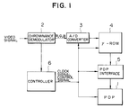
- the color display unit is provided with a PDP 1 for displaying, for example, a picture of a composite video signal composed of R, G and B signals and a synchronizing signal, a chrominance demodulator 2 for converting the video signal into R, G and B signals and, at the same time, for separating a synchronizing signal out of the video signal, an A/D converter 3 for analog-to-digital converting these converted R, G and B signals respectively, a ⁇ -ROM (storage means) 4 which is supplied with these digital-converted R, G and B signals from the A/D converter 3 and outputs corrected R, G and B signals obtained by applying gamma correction to the inputted digital-converted R, G and B signals, a PDP interface 5 including a controller and so on for driving the PDP 1 on the base of the gamma-corrected R, G and B signals supplied from the ⁇ -ROM 4, and a controller 6 for generating clock signals and control
- ⁇ -ROM 4 data required for gamma correction is stored in advance.
- the contrast ratio of the middle level upon which attention is given extremely on the screen of the PDP 1 is improved, and the gamma value corresponding to the luminance level on the same screen is made to be as large as possible within a range in which black and white of a picture are not collapsed, and within a range of tolerance limits in which any false outline of the picture is not so remarkable.
- the words "middle level” used herein means a level at a position, for example, in Fig.
- the ⁇ -ROM 4 stores ⁇ -correction data in which the gamma value at the middle portion of a gamma characteristic curve is set to be larger than 2.2, for example, 3, and at the same time, as shown in Fig. 3, the middle portion of the gamma characteristic curve is shifted to a position having a higher luminance level on the screen.
- the smoothness of the white and black foot portions of the gamma characteristic curve may be realized, for example, by making the gamma correction data have a biquadratic curve.
- a video signal of a picture to be displayed on the PDP 1 is being supplied into the chrominance demodulator 2.
- the R, G and B signals of the input video signal demodulated by the chrominance demodulator 2 are converted into digital signals in the A/D converter 3 respectively, and the data stored in the ⁇ -ROM 4 is read out by use of these digital signals as address signals. Since the above-mentioned gamma correction data are stored in this ⁇ -ROM 4 in advance, gamma-corrected signals may be read out in the form of data from the ⁇ -ROM 4. These output data are supplied to the PDP interface 5 which is a controller for the PDP 1, so that the PDP 1 is driven on the basis of the above-mentioned gamma-corrected signals.
- the data for deciding the gamma characteristics in the ⁇ -ROM 4 are such that the gamma value at the middle portion of the gamma characteristic curve is set be larger than 2.2, for example 3, (the broken line curve in Fig. 3 which is the same as the solid line curve in Fig. 2) to thereby enlarge the contrast ratio of the middle level which is most remarkable on the screen of the PDP 1.
- the lens aperture of a camera is adjusted so that the brightness at a portion at which attention is given or at which it is intended to give intensive expression on the screen is made to have an optimum value (that is, in the vicinity of the middle level).
- the middle portion of the gamma characteristic curve is shifted leftward in the same drawing (from the broken line curve to the solid line curve in Fig. 3), that is, the middle portion of the characteristic is shifted to a position having a higher luminance level on the screen, and the white and black foot portions of the gamma characteristic curve are made smooth (as shown by the solid line curve in Fig. 3). Accordingly, the average luminance of the screen of the PDP 1 becomes large, and the color saturation of the picture on the screen also becomes large, so that the picture can be displayed with clear colors.
- a color display unit with a plasma display panel can be used for a large-screen wall-mounted television set.
- gamma correction is performed by use of the ⁇ -ROM 4 in the above-mentioned embodiment, similar effects can be obtained even in the case where the ⁇ -ROM 4 is replaced by a suitable arithmetic means and the arithmetic means makes an arithmetic operation to obtain ⁇ -correction data every time when the arithmetic means is supplied with a signal from the A/D converter 3, so that gamma correction is performed with the obtained ⁇ -correction data.
- the gamma correction is performed with data in which a gamma value is made larger than 2.2 in the middle portion of a gamma characteristic curve, and, at the same time, the middle portion of the gamma characteristic curve is shifted to a position having a higher luminance level, and the white and black foot portions of the gamma characteristic curve are made smooth.
Applications Claiming Priority (3)
| Application Number | Priority Date | Filing Date | Title |
|---|---|---|---|
| JP6609493 | 1993-03-02 | ||
| JP05066094A JP3107260B2 (ja) | 1993-03-02 | 1993-03-02 | カラー表示装置 |
| JP66094/93 | 1993-03-02 |
Publications (3)
| Publication Number | Publication Date |
|---|---|
| EP0614321A2 true EP0614321A2 (de) | 1994-09-07 |
| EP0614321A3 EP0614321A3 (en) | 1996-10-16 |
| EP0614321B1 EP0614321B1 (de) | 1999-07-21 |
Family
ID=13305947
Family Applications (1)
| Application Number | Title | Priority Date | Filing Date |
|---|---|---|---|
| EP94301452A Expired - Lifetime EP0614321B1 (de) | 1993-03-02 | 1994-03-01 | Farbanzeigevorrichtung mit Plasmaanzeigetafel |
Country Status (6)
| Country | Link |
|---|---|
| US (1) | US5546101A (de) |
| EP (1) | EP0614321B1 (de) |
| JP (1) | JP3107260B2 (de) |
| AU (1) | AU675476B2 (de) |
| CA (1) | CA2116636C (de) |
| DE (1) | DE69419546T2 (de) |
Cited By (7)
| Publication number | Priority date | Publication date | Assignee | Title |
|---|---|---|---|---|
| EP0831643A2 (de) * | 1996-09-18 | 1998-03-25 | Matsushita Electric Industrial Co., Ltd. | Plasmaanzeigetafel und Verfahren zur Helligkeitskontrolle |
| EP0966165A1 (de) * | 1998-06-19 | 1999-12-22 | Pioneer Electronic Corporation | Videosignalverarbeitungsschaltung mit optimalem Signalpegel für invertierte Gammakorrektur |
| EP0992972A2 (de) * | 1998-10-01 | 2000-04-12 | LOEWE OPTA GmbH | Verfahren zur Einstellung der Helligkeit einer Zelle eines Flachdisplays |
| EP1065648A2 (de) * | 1999-06-30 | 2001-01-03 | Fujitsu Limited | Plasmaanzeigetafel |
| WO2001071701A2 (en) * | 2000-03-24 | 2001-09-27 | Lighthouse Technologies Ltd. | Selected data compression for digital pictorial information |
| EP1176834A2 (de) * | 2000-07-28 | 2002-01-30 | Fujitsu Hitachi Plasma Display Limited | Farbwiedergabekorrekturschaltung für Farbdarstellung und ein Farbanzeigerät |
| EP1130564A3 (de) * | 2000-02-29 | 2004-06-30 | Lg Electronics Inc. | Verfahren zur Regulierung der Farbtemperatur einer Plasmaanzeigetafel |
Families Citing this family (19)
| Publication number | Priority date | Publication date | Assignee | Title |
|---|---|---|---|---|
| JP3891499B2 (ja) * | 1995-04-14 | 2007-03-14 | パイオニア株式会社 | プラズマディスプレイパネルにおける輝度調整装置 |
| WO1997035294A1 (en) * | 1996-03-18 | 1997-09-25 | Philips Electronics N.V. | Plasma-addressed display |
| JPH10276349A (ja) * | 1997-03-27 | 1998-10-13 | Asahi Optical Co Ltd | 画像信号補正装置 |
| JPH11143379A (ja) * | 1997-09-03 | 1999-05-28 | Semiconductor Energy Lab Co Ltd | 半導体表示装置補正システムおよび半導体表示装置の補正方法 |
| US6285411B1 (en) * | 1997-10-10 | 2001-09-04 | Philips Electronics North America Corporation | Circuit for video moiré reduction |
| JP4189062B2 (ja) * | 1998-07-06 | 2008-12-03 | セイコーエプソン株式会社 | 電子機器 |
| EP1046307A1 (de) * | 1998-10-06 | 2000-10-25 | Matsushita Electric Industrial Co., Ltd. | Gammakorrekturschaltung und gammakorrekturverfahren |
| US6377270B1 (en) * | 1999-07-30 | 2002-04-23 | Microsoft Corporation | Method and system for transforming color coordinates by direct calculation |
| TW508560B (en) * | 2001-04-03 | 2002-11-01 | Chunghwa Picture Tubes Ltd | Method for performing different anti-compensation processes by segments on image gray levels inputted to plasma flat display |
| US6826303B2 (en) * | 2001-06-28 | 2004-11-30 | Hewlett-Packard Development Company, L.P. | Software-based acceleration color correction filtering system |
| JP3652352B2 (ja) * | 2001-12-27 | 2005-05-25 | エルジー電子株式会社 | フラットパネル表示装置の駆動方法及び装置 |
| KR100490405B1 (ko) * | 2002-07-02 | 2005-05-17 | 삼성전자주식회사 | 프린팅 시스템에 있어서 이미지의 색상 조정방법 및 이를위한 그래픽 사용자 인터페이스 |
| KR100493293B1 (ko) * | 2002-10-31 | 2005-06-02 | 엘지전자 주식회사 | 비선형 샘플링을 이용한 영상 신호의 감마 보정 방법 |
| KR20040041940A (ko) * | 2002-11-12 | 2004-05-20 | 삼성전자주식회사 | 액정 표시 장치 및 그 구동 방법 |
| US8289233B1 (en) | 2003-02-04 | 2012-10-16 | Imaging Systems Technology | Error diffusion |
| US8305301B1 (en) | 2003-02-04 | 2012-11-06 | Imaging Systems Technology | Gamma correction |
| KR100996412B1 (ko) * | 2004-05-14 | 2010-11-24 | 엘지전자 주식회사 | 플라즈마 디스플레이 패널의 계조 표현 장치 및 방법 |
| US8248328B1 (en) | 2007-05-10 | 2012-08-21 | Imaging Systems Technology | Plasma-shell PDP with artifact reduction |
| US8803922B2 (en) * | 2007-05-30 | 2014-08-12 | Apple Inc. | Methods and apparatuses for increasing the apparent brightness of a display |
Citations (1)
| Publication number | Priority date | Publication date | Assignee | Title |
|---|---|---|---|---|
| FR2656484A1 (fr) * | 1989-12-22 | 1991-06-28 | Thomson Csf | Dispositif de correction de gamma des signaux video destines a un ecran de visualisation et recepteur de television comportant un ecran recevant des signaux d'un tel dispositif. |
Family Cites Families (10)
| Publication number | Priority date | Publication date | Assignee | Title |
|---|---|---|---|---|
| US4020280A (en) * | 1973-02-21 | 1977-04-26 | Ryuichi Kaneko | Pulse width luminance modulation system for a DC gas discharge display panel |
| JPS5046216A (de) * | 1973-08-29 | 1975-04-24 | ||
| JPS53148918A (en) * | 1977-06-01 | 1978-12-26 | Hitachi Ltd | Matrix display unit |
| FR2612326A1 (fr) * | 1987-03-13 | 1988-09-16 | Thomson Csf | Procede de reglage des couleurs d'un panneau a plasma polychrome et panneau a plasma utilisant un tel procede |
| US5298892A (en) * | 1988-07-21 | 1994-03-29 | Proxima Corporation | Stacked display panel construction and method of making same |
| US5185602A (en) * | 1989-04-10 | 1993-02-09 | Cirrus Logic, Inc. | Method and apparatus for producing perception of high quality grayscale shading on digitally commanded displays |
| JPH0398086A (ja) * | 1989-09-11 | 1991-04-23 | Victor Co Of Japan Ltd | 液晶表示装置における残像打消回路 |
| JP2720607B2 (ja) * | 1990-03-02 | 1998-03-04 | 株式会社日立製作所 | 表示装置、階調表示方法及び駆動回路 |
| JPH04286492A (ja) * | 1991-03-15 | 1992-10-12 | Sharp Corp | テレビジョン受像機 |
| JPH04287592A (ja) * | 1991-03-18 | 1992-10-13 | Sanyo Electric Co Ltd | Museデコーダ |
-
1993
- 1993-03-02 JP JP05066094A patent/JP3107260B2/ja not_active Expired - Fee Related
-
1994
- 1994-02-24 US US08/201,376 patent/US5546101A/en not_active Expired - Fee Related
- 1994-02-25 AU AU56424/94A patent/AU675476B2/en not_active Ceased
- 1994-02-28 CA CA002116636A patent/CA2116636C/en not_active Expired - Fee Related
- 1994-03-01 DE DE69419546T patent/DE69419546T2/de not_active Expired - Fee Related
- 1994-03-01 EP EP94301452A patent/EP0614321B1/de not_active Expired - Lifetime
Patent Citations (1)
| Publication number | Priority date | Publication date | Assignee | Title |
|---|---|---|---|---|
| FR2656484A1 (fr) * | 1989-12-22 | 1991-06-28 | Thomson Csf | Dispositif de correction de gamma des signaux video destines a un ecran de visualisation et recepteur de television comportant un ecran recevant des signaux d'un tel dispositif. |
Cited By (19)
| Publication number | Priority date | Publication date | Assignee | Title |
|---|---|---|---|---|
| EP0831643A3 (de) * | 1996-09-18 | 1998-04-01 | Matsushita Electric Industrial Co., Ltd. | Plasmaanzeigetafel und Verfahren zur Helligkeitskontrolle |
| US6034656A (en) * | 1996-09-18 | 2000-03-07 | Matsushita Electric Industrial Co., Ltd. | Plasma display panel and method of controlling brightness of the same |
| EP0831643A2 (de) * | 1996-09-18 | 1998-03-25 | Matsushita Electric Industrial Co., Ltd. | Plasmaanzeigetafel und Verfahren zur Helligkeitskontrolle |
| EP1231779A3 (de) * | 1996-09-18 | 2002-11-27 | Matsushita Electric Industrial Co., Ltd. | Plasmaanzeigetafel und Verfahren zur Helligkeitskontrolle |
| EP1231779A2 (de) * | 1996-09-18 | 2002-08-14 | Matsushita Electric Industrial Co., Ltd. | Plasmaanzeigetafel und Verfahren zur Helligkeitskontrolle |
| US6271891B1 (en) | 1998-06-19 | 2001-08-07 | Pioneer Electronic Corporation | Video signal processing circuit providing optimum signal level for inverse gamma correction |
| EP0966165A1 (de) * | 1998-06-19 | 1999-12-22 | Pioneer Electronic Corporation | Videosignalverarbeitungsschaltung mit optimalem Signalpegel für invertierte Gammakorrektur |
| EP0992972A2 (de) * | 1998-10-01 | 2000-04-12 | LOEWE OPTA GmbH | Verfahren zur Einstellung der Helligkeit einer Zelle eines Flachdisplays |
| EP0992972A3 (de) * | 1998-10-01 | 2000-10-25 | LOEWE OPTA GmbH | Verfahren zur Einstellung der Helligkeit einer Zelle eines Flachdisplays |
| EP1065648A3 (de) * | 1999-06-30 | 2002-04-17 | Fujitsu Limited | Plasmaanzeigetafel |
| EP1065648A2 (de) * | 1999-06-30 | 2001-01-03 | Fujitsu Limited | Plasmaanzeigetafel |
| US7126562B1 (en) | 1999-06-30 | 2006-10-24 | Hitachi, Ltd. | Plasma display panel with constant color temperature or color deviation |
| EP1130564A3 (de) * | 2000-02-29 | 2004-06-30 | Lg Electronics Inc. | Verfahren zur Regulierung der Farbtemperatur einer Plasmaanzeigetafel |
| WO2001071701A2 (en) * | 2000-03-24 | 2001-09-27 | Lighthouse Technologies Ltd. | Selected data compression for digital pictorial information |
| WO2001071701A3 (en) * | 2000-03-24 | 2002-04-04 | Lighthouse Technologies Ltd | Selected data compression for digital pictorial information |
| AU2001250556B2 (en) * | 2000-03-24 | 2005-04-28 | Light-House Technologies Ltd. | Selected data compression for digital pictorial information |
| EP1176834A2 (de) * | 2000-07-28 | 2002-01-30 | Fujitsu Hitachi Plasma Display Limited | Farbwiedergabekorrekturschaltung für Farbdarstellung und ein Farbanzeigerät |
| EP1176834A3 (de) * | 2000-07-28 | 2004-11-03 | Fujitsu Hitachi Plasma Display Limited | Farbwiedergabekorrekturschaltung für Farbdarstellung und ein Farbanzeigerät |
| US6940559B2 (en) | 2000-07-28 | 2005-09-06 | Fujitsu Hitachi Plasma Display Limited | Color reproduction correction circuit for color representation and a color display |
Also Published As
| Publication number | Publication date |
|---|---|
| AU5642494A (en) | 1994-09-08 |
| CA2116636A1 (en) | 1994-09-03 |
| DE69419546D1 (de) | 1999-08-26 |
| AU675476B2 (en) | 1997-02-06 |
| JPH06261335A (ja) | 1994-09-16 |
| CA2116636C (en) | 2000-10-17 |
| EP0614321B1 (de) | 1999-07-21 |
| EP0614321A3 (en) | 1996-10-16 |
| US5546101A (en) | 1996-08-13 |
| JP3107260B2 (ja) | 2000-11-06 |
| DE69419546T2 (de) | 2000-03-30 |
Similar Documents
| Publication | Publication Date | Title |
|---|---|---|
| US5546101A (en) | Color display unit with plasma display panel | |
| US5347294A (en) | Image display apparatus | |
| US5257103A (en) | Method and apparatus for deinterlacing video inputs | |
| US20040257318A1 (en) | Image display apparatus | |
| JPH0564110A (ja) | 映像信号補正装置とそれを用いた表示装置 | |
| US7161608B2 (en) | Digital system and method for displaying images using shifted bit-weights for neutral density filtering applications | |
| JPH07121138A (ja) | 時分割カラー液晶表示装置及びその駆動方法 | |
| JP2001042833A (ja) | カラー表示装置 | |
| JP2006153914A (ja) | 液晶プロジェクタ装置 | |
| JPH02271389A (ja) | フルカラー液晶表示装置 | |
| JPH11338407A (ja) | 固定画素表示装置及びその駆動方法 | |
| WO2007009057A1 (en) | Displaying non-linear images on linear displays | |
| US7205961B1 (en) | Display apparatus having uniformity function of pixel luminescence frequency and display method | |
| US7307611B2 (en) | Driving method for LCD panel | |
| JPH1198521A (ja) | 表示方法及び投写型表示装置 | |
| JPH0990905A (ja) | Ledディスプレイの表示方法 | |
| WO1995026109A1 (fr) | Procede de pilotage d'un afficheur a cristaux liquides | |
| KR20050055252A (ko) | 액정표시장치 및 그 구동방법 | |
| JPH10319895A (ja) | 表示装置、表示方法および表示制御プログラムを記録した媒体 | |
| JPH08317321A (ja) | 画像表示装置 | |
| JP3292256B2 (ja) | プラズマ表示駆動装置 | |
| US5235429A (en) | Display apparatus having bandwidth reduction and vertical interpolation | |
| KR100296417B1 (ko) | 블랙화면의 화질 보정장치 | |
| JPH0294868A (ja) | 映像補正回路 | |
| JPH0955907A (ja) | 表示装置 |
Legal Events
| Date | Code | Title | Description |
|---|---|---|---|
| PUAI | Public reference made under article 153(3) epc to a published international application that has entered the european phase |
Free format text: ORIGINAL CODE: 0009012 |
|
| AK | Designated contracting states |
Kind code of ref document: A2 Designated state(s): DE FR GB IT |
|
| PUAL | Search report despatched |
Free format text: ORIGINAL CODE: 0009013 |
|
| AK | Designated contracting states |
Kind code of ref document: A3 Designated state(s): DE FR GB IT |
|
| 17P | Request for examination filed |
Effective date: 19961206 |
|
| GRAG | Despatch of communication of intention to grant |
Free format text: ORIGINAL CODE: EPIDOS AGRA |
|
| 17Q | First examination report despatched |
Effective date: 19980914 |
|
| GRAG | Despatch of communication of intention to grant |
Free format text: ORIGINAL CODE: EPIDOS AGRA |
|
| GRAH | Despatch of communication of intention to grant a patent |
Free format text: ORIGINAL CODE: EPIDOS IGRA |
|
| GRAH | Despatch of communication of intention to grant a patent |
Free format text: ORIGINAL CODE: EPIDOS IGRA |
|
| GRAA | (expected) grant |
Free format text: ORIGINAL CODE: 0009210 |
|
| AK | Designated contracting states |
Kind code of ref document: B1 Designated state(s): DE FR GB IT |
|
| REF | Corresponds to: |
Ref document number: 69419546 Country of ref document: DE Date of ref document: 19990826 |
|
| ET | Fr: translation filed | ||
| ITF | It: translation for a ep patent filed |
Owner name: MODIANO & ASSOCIATI S.R.L. |
|
| PLBE | No opposition filed within time limit |
Free format text: ORIGINAL CODE: 0009261 |
|
| STAA | Information on the status of an ep patent application or granted ep patent |
Free format text: STATUS: NO OPPOSITION FILED WITHIN TIME LIMIT |
|
| 26N | No opposition filed | ||
| REG | Reference to a national code |
Ref country code: GB Ref legal event code: IF02 |
|
| PGFP | Annual fee paid to national office [announced via postgrant information from national office to epo] |
Ref country code: DE Payment date: 20070222 Year of fee payment: 14 |
|
| PGFP | Annual fee paid to national office [announced via postgrant information from national office to epo] |
Ref country code: GB Payment date: 20070228 Year of fee payment: 14 |
|
| PGFP | Annual fee paid to national office [announced via postgrant information from national office to epo] |
Ref country code: IT Payment date: 20070608 Year of fee payment: 14 |
|
| PGFP | Annual fee paid to national office [announced via postgrant information from national office to epo] |
Ref country code: FR Payment date: 20070308 Year of fee payment: 14 |
|
| GBPC | Gb: european patent ceased through non-payment of renewal fee |
Effective date: 20080301 |
|
| REG | Reference to a national code |
Ref country code: FR Ref legal event code: ST Effective date: 20081125 |
|
| PG25 | Lapsed in a contracting state [announced via postgrant information from national office to epo] |
Ref country code: DE Free format text: LAPSE BECAUSE OF NON-PAYMENT OF DUE FEES Effective date: 20081001 |
|
| PG25 | Lapsed in a contracting state [announced via postgrant information from national office to epo] |
Ref country code: FR Free format text: LAPSE BECAUSE OF NON-PAYMENT OF DUE FEES Effective date: 20080331 |
|
| PG25 | Lapsed in a contracting state [announced via postgrant information from national office to epo] |
Ref country code: GB Free format text: LAPSE BECAUSE OF NON-PAYMENT OF DUE FEES Effective date: 20080301 |
|
| PG25 | Lapsed in a contracting state [announced via postgrant information from national office to epo] |
Ref country code: IT Free format text: LAPSE BECAUSE OF NON-PAYMENT OF DUE FEES Effective date: 20080301 |