EP0611121A2 - Verfahren zum Mustern von Dielektrikum und resultierende Strukturen - Google Patents
Verfahren zum Mustern von Dielektrikum und resultierende Strukturen Download PDFInfo
- Publication number
- EP0611121A2 EP0611121A2 EP94300881A EP94300881A EP0611121A2 EP 0611121 A2 EP0611121 A2 EP 0611121A2 EP 94300881 A EP94300881 A EP 94300881A EP 94300881 A EP94300881 A EP 94300881A EP 0611121 A2 EP0611121 A2 EP 0611121A2
- Authority
- EP
- European Patent Office
- Prior art keywords
- layer
- dielectric layer
- dielectric
- opening
- providing
- Prior art date
- Legal status (The legal status is an assumption and is not a legal conclusion. Google has not performed a legal analysis and makes no representation as to the accuracy of the status listed.)
- Withdrawn
Links
Images


Classifications
-
- H—ELECTRICITY
- H05—ELECTRIC TECHNIQUES NOT OTHERWISE PROVIDED FOR
- H05K—PRINTED CIRCUITS; CASINGS OR CONSTRUCTIONAL DETAILS OF ELECTRIC APPARATUS; MANUFACTURE OF ASSEMBLAGES OF ELECTRICAL COMPONENTS
- H05K3/00—Apparatus or processes for manufacturing printed circuits
- H05K3/0011—Working of insulating substrates or insulating layers
- H05K3/0017—Etching of the substrate by chemical or physical means
- H05K3/0041—Etching of the substrate by chemical or physical means by plasma etching
-
- H10P50/287—
-
- H10W20/081—
-
- H10W70/093—
-
- H10W70/095—
-
- H10W70/614—
-
- H—ELECTRICITY
- H05—ELECTRIC TECHNIQUES NOT OTHERWISE PROVIDED FOR
- H05K—PRINTED CIRCUITS; CASINGS OR CONSTRUCTIONAL DETAILS OF ELECTRIC APPARATUS; MANUFACTURE OF ASSEMBLAGES OF ELECTRICAL COMPONENTS
- H05K1/00—Printed circuits
- H05K1/02—Details
- H05K1/03—Use of materials for the substrate
- H05K1/0313—Organic insulating material
- H05K1/0353—Organic insulating material consisting of two or more materials, e.g. two or more polymers, polymer + filler, + reinforcement
- H05K1/036—Multilayers with layers of different types
-
- H—ELECTRICITY
- H05—ELECTRIC TECHNIQUES NOT OTHERWISE PROVIDED FOR
- H05K—PRINTED CIRCUITS; CASINGS OR CONSTRUCTIONAL DETAILS OF ELECTRIC APPARATUS; MANUFACTURE OF ASSEMBLAGES OF ELECTRICAL COMPONENTS
- H05K2201/00—Indexing scheme relating to printed circuits covered by H05K1/00
- H05K2201/01—Dielectrics
- H05K2201/0137—Materials
- H05K2201/0166—Polymeric layer used for special processing, e.g. resist for etching insulating material or photoresist used as a mask during plasma etching
-
- H—ELECTRICITY
- H05—ELECTRIC TECHNIQUES NOT OTHERWISE PROVIDED FOR
- H05K—PRINTED CIRCUITS; CASINGS OR CONSTRUCTIONAL DETAILS OF ELECTRIC APPARATUS; MANUFACTURE OF ASSEMBLAGES OF ELECTRICAL COMPONENTS
- H05K2201/00—Indexing scheme relating to printed circuits covered by H05K1/00
- H05K2201/01—Dielectrics
- H05K2201/0183—Dielectric layers
- H05K2201/0195—Dielectric or adhesive layers comprising a plurality of layers, e.g. in a multilayer structure
-
- H—ELECTRICITY
- H05—ELECTRIC TECHNIQUES NOT OTHERWISE PROVIDED FOR
- H05K—PRINTED CIRCUITS; CASINGS OR CONSTRUCTIONAL DETAILS OF ELECTRIC APPARATUS; MANUFACTURE OF ASSEMBLAGES OF ELECTRICAL COMPONENTS
- H05K3/00—Apparatus or processes for manufacturing printed circuits
- H05K3/0011—Working of insulating substrates or insulating layers
- H05K3/0017—Etching of the substrate by chemical or physical means
- H05K3/0026—Etching of the substrate by chemical or physical means by laser ablation
- H05K3/0032—Etching of the substrate by chemical or physical means by laser ablation of organic insulating material
-
- H10W70/099—
-
- H10W70/60—
-
- H10W70/682—
-
- H10W72/01255—
-
- H10W72/073—
-
- H10W72/29—
-
- H10W72/874—
-
- H10W72/9413—
-
- H10W90/00—
-
- H10W90/734—
-
- Y—GENERAL TAGGING OF NEW TECHNOLOGICAL DEVELOPMENTS; GENERAL TAGGING OF CROSS-SECTIONAL TECHNOLOGIES SPANNING OVER SEVERAL SECTIONS OF THE IPC; TECHNICAL SUBJECTS COVERED BY FORMER USPC CROSS-REFERENCE ART COLLECTIONS [XRACs] AND DIGESTS
- Y10—TECHNICAL SUBJECTS COVERED BY FORMER USPC
- Y10S—TECHNICAL SUBJECTS COVERED BY FORMER USPC CROSS-REFERENCE ART COLLECTIONS [XRACs] AND DIGESTS
- Y10S438/00—Semiconductor device manufacturing: process
- Y10S438/94—Laser ablative material removal
-
- Y—GENERAL TAGGING OF NEW TECHNOLOGICAL DEVELOPMENTS; GENERAL TAGGING OF CROSS-SECTIONAL TECHNOLOGIES SPANNING OVER SEVERAL SECTIONS OF THE IPC; TECHNICAL SUBJECTS COVERED BY FORMER USPC CROSS-REFERENCE ART COLLECTIONS [XRACs] AND DIGESTS
- Y10—TECHNICAL SUBJECTS COVERED BY FORMER USPC
- Y10S—TECHNICAL SUBJECTS COVERED BY FORMER USPC CROSS-REFERENCE ART COLLECTIONS [XRACs] AND DIGESTS
- Y10S438/00—Semiconductor device manufacturing: process
- Y10S438/942—Masking
- Y10S438/945—Special, e.g. metal
Definitions
- This invention relates generally to patterning of polymers. More particularly, this invention relates to patterning of polymers in a high density interconnect process in such a way as to allow use of low dielectric constant polymers, and to remove any polymer ridges which may be formed around pattern openings.
- Teflon polytetrafluoroethylene Teflon is a trademark of E.I. duPont de Nemours and Co.
- fluorocarbon polymers have highly desirable properties in the manufacture of high density interconnect (HDI) circuits.
- Polytetrafluoroethylene has one of the lowest dielectric constants in the polymer field, optical clarity, and excellent chemical and temperature stability.
- laser patterning of fluorocarbon polymers is hindered because the various fluorocarbon polymer derivatives are transparent to light of wavelengths generally greater than 200 nm.
- CW continuous wave
- fluorocarbon polymers in conventional procedures is the fact that metal does not readily adhere to the surface. Thus, it is difficult to pattern electrical connections on a polytetrafluoroethylene surface.
- high dielectric constant materials limits the present HDI process. Specifically, high dielectric constant materials (i.e., ⁇ about 3.0) applied over chips contribute additional capacitance loading to the chips at high frequencies and thus alter the design performance of the chips. Improved propagation and reduced capacitive coupling are obtained with Teflon polytetrafluoroethylene ( ⁇ about 2.0) because of its significantly lower dielectric constant. Additionally, video array chips need to have their viewing windows cleared of light blocking polymer materials to achieve proper optical response. Localized ablation has been used to clear polymers off of sensitive areas of chips; however, direct laser ablation on the chip surface sometimes damages the chip. Since Teflon polytetrafluoroethylene is transparent down to 200 nm, this ablation damage can be reduced while still achieving optically clear layers.
- Polymers that absorb light at wavelengths of approximately 350-360 nm work well with this CW argon ion laser system.
- the laser energy is absorbed by the polymer and locally heats the polymer to temperatures where thermal decomposition or ablation occurs.
- fluorocarbon polymers such as polytetrafluoroethylene
- polytetrafluoroethylene has essentially no absorption at wavelengths above 200 nm, both CW and pulsed excimer lasers at all wavelengths above 200 nm will not effectively ablate this material, thus limiting its use as a low dielectric constant interlayer dielectric for HDI adaptive lithography in which an adaptive laser is employed for via fabrication.
- the process of via formation by adaptive lithography using laser dithering can cause extreme localized heating of the surrounding polymer and can put the polymer under stress and result in melting or flowing of the material.
- the stress caused by via dithering often results in the formation of a substantial polymer ridge around the surface perimeter of the via.
- Exposure of the via to excimer lasers or ashing procedures replicates the surface topography further down into the polymer, leaving the ridge intact.
- Subsequent metallization causes a much larger metal ridge to form around the via perimeter because of excessive electroplating in this area, due to high electric field density areas.
- Subsequent patterning of the metal around the via becomes difficult because of thin or incomplete resist coverage over the metal ridge, allowing etchants to attack the via metal. Additionally, the metal ridge can form shorts between metal levels, due to thinning of dielectrics.
- one object of the invention is to provide a patternable integral mask (preferably using adaptive lithography) that enables the patterning of non-laser absorbing materials such as polytetrafluoroethylene and other fluorinated polyethylenes.
- Another object of the invention is to provide a method of fabricating low dielectric constant structures for use as high density interconnect layers in multi-chip module applications.
- Still another object of the invention is to provide a method of fabricating structures suitable for use in video arrays.
- Yet another object of the invention is to provide a process for adhering metal to a dielectric layer consisting essentially of material to which the metal under normal use does not adhere.
- Another object of the invention is to provide a method to remove the dielectric ridge which forms around a via surface perimeter in a dielectric layer during laser dithering.
- the invention accomplishes the above objects by employing a differentiable ablation method of patterning materials which are not all of the same absorbance using, in one embodiment, an absorbant material, such as Kapton polyimide, over a non-absorbant material, such as Teflon polytetrafluoroethylene.
- Kapton polyimide is easily patterned by the adaptive lithography method, and this patterned polyimide becomes an integral mask that enables precision, selective, differential etching by methods such as RIE (reactive ion etching) of the underlying, nonablated material.
- RIE reactive ion etching
- a non-absorbant material such as silicon nitride, may overlie the absorbant layer.
- This overlying non-absorbant material is patterned simultaneously with the absorbant layer by the adaptive lithography method, and these patterned layers become an integral mask that enables precision, selective, differential etching by methods such as RIE of both the absorbant material and the underlying non-absorbant material.
- an opening is fabricated in a first dielectric layer which is not itself laser ablatable at a given laser wavelength by providing a second dielectric layer which is laser ablatable at the given laser wavelength overlying the first dielectric layer.
- An opening is provided in the second dielectric layer by laser ablation.
- An opening aligned with the opening in the second dielectric layer is etched in the first dielectric layer, using the second layer as an etch mask.
- an inorganic optically transparent mask is deposited over an optically absorbing polymer material overlying an optically non-absorbing polymer material to form a structure that is patternable by an adaptive masking technique.
- Laser ablation patterning of the absorbing polymer material ablates the overlying mask in the same area, providing an integral opening.
- An opening is etched in the nonabsorbing polymer material, aligned with the opening in the absorbing polymer material, without loss of dielectric thickness.
- an inorganic optically transparent hard mask is deposited over an ablatable polymer material to form a structure that is patternable by an adaptive masking technique.
- This method is used for removing a polymer ridge formed around a via surface.
- a via is provided through the hard mask and polymer layer.
- the exposed portion of the polymer layer in the area of the hard mask is isotropically etched.
- the hard mask is then removed from the polymer layer.
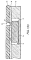
- FIG. 1(a) is a sectional side view of a chip 12 with pads 14 attached to a substrate 10 in well 16.
- Chip 12 may comprise an integrated circuit chip or a discrete circuit component and can be attached to the substrate by adhesive 15.
- Substrate 10 may comprise any structural material and, in a preferred embodiment, comprises a ceramic such as alumina.
- the chip and substrate are overlaid by a first dielectric layer 18, which, in turn, is overlaid by a second dielectric layer 20.
- First dielectric 18 has a lower dielectric constant than second dielectric layer 20.
- Second dielectric layer 20 is selected to be ablatable at commercially available laser wavelengths and in one embodiment may comprise Kapton polyimide.
- First dielectric layer 18 with low dielectric constant and low optical absorption above 200 nm, is not ablatable at commercially available laser wavelengths in the 350-360 nm range.
- first dielectric layer 18 may comprise Teflon polytetrafluoroethylene. Additional examples of materials for first dielectric layer 18 include polyesters and other fluorocarbon polymers.
- the two layers 18 and 20 may comprise a double laminate film, such as Dupont F type and XP type Kapton polyimide-Teflon polytetrafluoroethylene products.
- a double laminate film such as Dupont FEP and PFA series Teflon polytetrafluoroethylene may be covered by a layer of Kapton polyimide, or liquid Teflon polytetrafluoroethylene such as Dupont AF series may be used in combination with a high absorbance film or a spun-on high absorbance material such as silicone polyimide or Ultem polyetherimide resin (Ultem is a registered trademark of General Electric Company, Pittsfield, MA).
- FIG. 1(b) is a view similar to that of FIG. 1(a), with a laser dithered hole 22 through second dielectric layer 20.
- Methods for laser dithering are disclosed in Eichelberger et al., U.S. Pat. No. 4,783,695, issued Nov. 8, 1988, and Eichelberger et al., U.S. Pat. No. 4,894,115, issued Jan. 16, 1990, both of which are commonly assigned and herein incorporated by reference. Because of the different absorbancies of the materials, when second dielectric layer 20 is laser dithered, the first dielectric layer 18 is undisturbed.
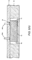
- FIG. 1(c) is a view similar to that of FIG. 1(b), with an opening extending through both second dielectric layer 20 and first dielectric layer 18.
- the opening is a via 24 exposing chip pad 14; the invention, however, extends to any type of opening, including large area openings, and is not limited to vias.
- this opening through first dielectric layer 18 is formed by RIE (reactive ion etching).
- RIE reactive ion etching
- the entire top surface of the second dielectric layer 20 is exposed and thus etched to result in a thinner second dielectric layer.
- the resulting thickness of second dielectric layer 20 can be controlled by adjusting the initial thickness as well as RIE etch time or etch chemistry.
- HDI assemblies are generally exposed to an O2/CF4 plasma before metallization to clear laser debris. RIE accomplishes removal of laser soot while etching through first dielectric layer 18.
- first dielectric layer 18 comprises Teflon polytetrafluoroethylene, 0.5 mil thick
- second dielectric layer 20 comprises Kapton polyimide, 1.0 mil thick
- an Anelva RIE etcher model 506 was used to remove first dielectric layer 18, using a laser dithered second dielectric layer 20 as a mask.
- a three step etch sequence was used to produce vias in an integrated circuit (IC) test structure.
- IC integrated circuit
- a mixture of 90% CF4 and 10% O2 total flow of 40 standard cubic centimeters per minute (sccm); power of 500 watts (W); pressure of 155 millitorr (mtorr); time of 10 minutes
- sccm standard cubic centimeters per minute
- W power of 500 watts
- mtorr millitorr
- time of 10 minutes was used to remove both soot from the laser dithering operation and remaining residual Kapton polyimide at the bottom of the via, yielding a clear Teflon area to etch.
- This plasma condition resulted in an etch rate ratio of approximately 1:1 for Kapton polyimide (1370 ⁇ /min) and Teflon polytetrafluoroethylene (1400 ⁇ /min).
- a plasma condition with a more selective etch rate ratio to Teflon polytetrafluoroethylene was used in order to preserve the Kapton polyimide mask (second dielectric layer 20), while removing the entire thickness of Teflon polytetrafluoroethylene (first dielectric layer 18) from the bottom of the via.
- An Ar plasma etch total flow of 40 sccm; power of 600 W; pressure of 50 mtorr; time of 60 minutes
- a mixture of 50% O2 and 50% Ar (total flow of 40 sccm; power of 600 W; pressure of 30 mtorr; time of 20 minutes) was used to remove residual Teflon polytetrafluoroethylene and to thin the upper Kapton polyimide layer 20 at a fast rate.
- This plasma condition resulted in an etch rate ratio of approximately 1.25:1 for Teflon polytetrafluoroethylene (3473 ⁇ /min) and Kapton polyimide (2780 ⁇ /min).
- the three step etch sequence yielded vias with openings approximately 2 mil square, and a final total dielectric film thickness of approximately 1 mil (0.5 mil Teflon polytetrafluoroethylene and 0.5 mil Kapton polyimide).
- a top metallization comprising 1000 ⁇ Ti, 4000 ⁇ Cu, 4 ⁇ m of electroplated copper and 1000 ⁇ Ti was deposited using conventional sputtering and electroplating techniques.
- low contact resistance (2-5 milliohms) was measured between the upper Ti/Cu/Ti and the metal pad 14, which generally comprises Al, at the bottom of the via, indicating that dielectric layers 18 and 20 were completely removed from the metal pad and the via was free of residue.
- the third step in the etch sequence can be used in other embodiments to remove or greatly thin second dielectric layer 20, leaving a surface which provides good adhesion to other low dielectric constant layers such as benzocyclobutene (BCB), fluorocarbon polymers such as Teflon polytetrafluoroethylene, or metal.
- BCB benzocyclobutene
- fluorocarbon polymers such as Teflon polytetrafluoroethylene, or metal.
- FIG. 1(d) is a view similar to that of FIG. 1(c), with an electrically conducting material 28 now situated in via 24.
- Aforementioned U.S. Pat. No. 4,783,695 discloses the basic HDI techniques.
- FIG. 1(e) is a view similar to that of FIG. 1(a), with a third dielectric layer 19 situated between first dielectric layer 18 and chip 12.
- adhesives such as first dielectric layer 18, in the embodiment shown in FIGs. 1(a)-1(d), can flow, resulting in non-uniform adhesive thickness and thus in non-uniform dielectric layers after processing.
- the use of first dielectric layer 18 and second dielectric layer 20 (which acts as a mask), such as type XP type Dupont film composite laminates, may be enhanced in usage by inserting a third dielectric layer 19 which has a low dielectric constant and lower melting point than first layer 18 (which also has a low dielectric constant) between the first layer and the substrate.
- This structure may comprise, for example, a Dupont type FEP Teflon polytetrafluoroethylene that is placed as a film (or prelaminated to an XP double laminate film) under the type XP film.
- the FEP Teflon polytetrafluoroethylene may melt, flow, or be forced away by the lamination process at corners of the die or other sharp edged areas.
- the use of two layers of Teflon polytetrafluoroethylene, or two layers other low dielectric constant films, with differing melting points provides a guaranteed minimum thickness of material between chip 12 and dielectric layers 18 and 20, thus providing uniform dielectric properties.
- second dielectric layer 20 may be replaced by any appropriate masking material which can be removed without damaging the module, such as, for example, an electrically conductive material.
- a hard mask 76 shown in FIG. 3(a) may be added to the configuration of FIG. 1(e), as discussed infra .
- FIG. 2 is a sectional side view of a laser ablated window 32 in second dielectric layer 20, overlying first dielectric layer 18, overlying a chip 30 in well 16 in substrate 10.
- the laser ablated window through second dielectric layer 20 is situated over a damage sensitive area 34, such as a video array area or a high frequency area.
- a laser may be used to locally ablate second dielectric layer 20 down to first dielectric layer 18. This is usually sufficient for optical and dielectric constraints, especially because a video array is preferably covered by a protective layer to prevent damage. If the laser process or RIE has affected the optical clarity of first dielectric layer 18, optical clarity may be adjusted with localized heat reflow, which smooths the surface of first dielectric layer 18 in window 32.
- the configurations of FIGs. 1(a)-1(d) further include a hard mask 76 which overlies first dielectric layer 18 and second dielectric layer 20.
- Metal contact 17 may be either a chip pad or a selected portion of an electrically conductive interconnect pattern.
- hard mask 76 an oxygen plasma resistant layer, preferably transparent, is deposited on top of an HDI module (not shown) after application of dielectric layers 18 and 20.
- Silicon nitride is one useful material for hard mask 76 because the nitride mask is transparent to allow visual alignment to the substrate during via dither; it has good adhesion to polymer surfaces; it has a very low erosion rate during polymer etching; and it is easily removed.
- the nitride film is deposited from silane and ammonia source gases using low pressure, plasma enhanced chemical vapor deposition at 200°C. This technique is compatible with other HDI processing steps.
- nitride layer hard mask 76
- laser dithering for via formation is performed as discussed with reference to FIG. 1(b), and dielectric ridge 80 is formed, as shown in FIG. 3(b).
- the nitride film is removed at the same time and in the same area during the laser ablation of second dielectric layer 20 directly over via 23, as shown in FIG. 3(b) .
- first dielectric layer 18 may be etched in the same manner as discussed with respect to FIG. 1(c), leaving a via opening 25, shown in FIG. 3(c) , extending through dielectric layers 18 and 20 to metal contact 17.
- hard mask 76 can be used as a mask to plasma etch out the remainder of the polymer in the via without decreasing the total thickness of second dielectric layer 20.
- Hard mask 76 thus provides uniform dielectric layers with controlled thicknesses, enabling better impedance matching for stripline devices.
- ridge 80 is subsequently removed during the etch of first dielectric layer 18.
- a second etch process removes hard mask 76 from the surface of second dielectric layer 20, as shown in FIG. 3(d) .
- this can be performed with RIE using a mixture of 90% CF4 and 10% O2 ( total flow of 39 sccm; power of 400 W; and pressure of 155 mtorr).
- the HDI module is then ready for continuation of fabrication, with no additional cleaning required. Additionally, this etch promotes good adhesion between the surface of second dielectric layer 20 and subsequent sputtered metal layers (not shown). Both the polymer ridge removal and hard mask removal etch steps can be done consecutively in a RIE system for ease of implementation.
- a hard mask layer 76 is also useful for removing polymer dielectric ridges which may form during via fabrication by laser dithering layers that are laser ablatable.
- FIGs. 4(a) through 4(c) illustrate a process for removing a dielectric ridge 80 formed during laser dithering of dielectric layer 82, which in one embodiment comprises Kapton polyimide.
- FIG. 4(a) is a view showing the ridge that results from dithering.
- FIG. 4(b) is a view of the via 74 which results after a short isotropic etch in a barrel type etcher using 9% CF4 and 91% O2 (total flow 600 sccm; power of 150 W; and pressure of 750 mtorr).
- the etch process isoptropically etches the exposed Kapton polyimide selective to the hard mask, effectively undercutting the hard mask surrounding the vias, and completely removing the polymer dielectric ridge. Because the isotropic etch process etches more dielectric at the opening of the via than in the chip pad area, a taper 220 is created, the size and nature of which depend on the plasma pressure. The taper can thus be designed to obtain improved metal step coverage.
- FIG. 4(c) is a view after the hard mask shown in FIG. 4(b) has been removed in the same manner as discussed with respect to FIG. 3(d).
- patterning low dielectric constant layers may be performed by using an inert mask layer 38 comprising metals or other hard materials such as nitrides or oxides rather than a polymeric dielectric layer 20 (shown in FIGs. 1(a)-1(d)).
- the inert mask material is chosen so that it will not react during the etching of the low dielectric constant layer.
- FIG. 5(a) is a sectional side view of chip 12 in a substrate 10, in well 16 covered by low dielectric constant layer 18, which, in turn, is covered by a layer of inert mask material 38, which itself is covered by a layer of photoresist 40.
- a Kapton polyimide/Teflon polytetrafluoroethylene layer may be laminated as discussed with respect to FIG. 1(a).
- the entire Kapton polyimide portion can be removed using RIE or other plasma or chemical treatments. It is preferable to leave a thin film of Kapton polyimide (not shown) on the Teflon polytetrafluoroethylene layer to improve mask adhesion. Concentrated H2SO4, NaOH, etc., may be used in lieu of RIE and will etch Kapton polyimide quickly. These treatments may shorten RIE time and protect the circuit during this processing.
- low dielectric constant layer 18 may be applied as the only dielectric layer, although applying Teflon polytetrafluoroethylene alone is more difficult than using a prefabricated double layer film such as Kapton polyimide/Teflon polytetrafluoroethylene.
- inert mask 38 comprises a metal mask.
- the module can be metallized with 1000 ⁇ titanium/tungsten (TiW) or titanium (Ti), for adhesion, and metallized with 1000-4000 ⁇ of molybdenum, for example.
- the thickness depends on the surface finish and topography of the module being processed.
- the object is to use a metal system that is non-reactive in the etch chemistry used to remove the dielectric material.
- the metal inert mask also needs to be removed selective to Al chip pads.
- the metallized module is coated with a photoresist and patterned with adaptive lithography (both these techniques are disclosed in aforementioned U.S. Pat. No. 4,835,704).
- the photoresist is developed and rinsed, resulting in a pattern with openings 42 as shown in FIG. 5(b) .
- the metal mask is then etched to create openings 44 and the photoresist is removed to expose the low dielectric constant layer 18 to be etched, as shown in FIG. 5(c) .
- the via 44 shown in FIG. 5(d) , can be etched using a mixture of 50% O2 and 50% Ar, as described with reference to FIG. 1(c).
- second dielectric layer 20 in the approach described in conjunction with FIGs.
- FIG. 5(e) is a view similar to that of FIG. 5(d), with the inert mask removed.
- the inert mask is a metal such as Ti/Mo or TiW/Mo, it can be removed selectively to the Al chip pads 14 with RIE using a mixture of 70% SF6 and 30% O2 (total flow 60 sccm; power 300 W; and pressure 65 mtorr).
- other metals such as Ti/Al are used as the mask, chip pads 14 must be protected from the mask etch.
- One protection process is to re-photoresist the module with photoresist layer 200 (shown in FIG. 5(f)) and use the HDI adaptive lithography system, disclosed in aforementioned U.S. Pat. No.
- Another method for protecting chip pads during the inert mask etch is to stop the RIE prior to completion of the via etch and remove the mask, using low dielectric constant layer 18 as the etch mask.
- the module is then returned to the RIE process and etched to via completion. This process completely etches the via and also differentially etches the thickness of the remaining low dielectric constant layer 18 everywhere else.
Landscapes
- Engineering & Computer Science (AREA)
- Physics & Mathematics (AREA)
- Plasma & Fusion (AREA)
- Manufacturing & Machinery (AREA)
- Microelectronics & Electronic Packaging (AREA)
- Drying Of Semiconductors (AREA)
- Internal Circuitry In Semiconductor Integrated Circuit Devices (AREA)
- Laser Beam Processing (AREA)
Applications Claiming Priority (2)
| Application Number | Priority Date | Filing Date | Title |
|---|---|---|---|
| US14609 | 1993-02-08 | ||
| US08/014,609 US5302547A (en) | 1993-02-08 | 1993-02-08 | Systems for patterning dielectrics by laser ablation |
Publications (2)
| Publication Number | Publication Date |
|---|---|
| EP0611121A2 true EP0611121A2 (de) | 1994-08-17 |
| EP0611121A3 EP0611121A3 (de) | 1995-03-22 |
Family
ID=21766510
Family Applications (1)
| Application Number | Title | Priority Date | Filing Date |
|---|---|---|---|
| EP94300881A Withdrawn EP0611121A3 (de) | 1993-02-08 | 1994-02-07 | Verfahren zum Mustern von Dielektrikum und resultierende Strukturen. |
Country Status (3)
| Country | Link |
|---|---|
| US (1) | US5302547A (de) |
| EP (1) | EP0611121A3 (de) |
| JP (1) | JPH077102A (de) |
Cited By (3)
| Publication number | Priority date | Publication date | Assignee | Title |
|---|---|---|---|---|
| LT5900B (lt) | 2011-06-16 | 2013-02-25 | Uab "Precizika - Met Sc" | Būdas nuimti sixny ploną sluoksnį nuo si paviršiaus nepažeidžiant p/n legiruoto si sluoksnio |
| CN111508820A (zh) * | 2020-03-25 | 2020-08-07 | 长江存储科技有限责任公司 | 清洗方法 |
| WO2022028852A1 (de) * | 2020-08-03 | 2022-02-10 | Gebr. Schmid Gmbh | Verfahren zur leiterplattenherstellung |
Families Citing this family (51)
| Publication number | Priority date | Publication date | Assignee | Title |
|---|---|---|---|---|
| US5468561A (en) * | 1993-11-05 | 1995-11-21 | Texas Instruments Incorporated | Etching and patterning an amorphous copolymer made from tetrafluoroethylene and 2,2-bis(trifluoromethyl)-4,5-difluoro-1,3-dioxole (TFE AF) |
| DE69424393T2 (de) * | 1993-12-28 | 2001-02-15 | Nec Corp., Tokio/Tokyo | Verfahren zur Bildung von Kontaktbohrungen in einer isolierenden Membran und Verfahren zum Schneiden der Membran |
| US5785787A (en) | 1994-05-23 | 1998-07-28 | General Electric Company | Processing low dielectric constant materials for high speed electronics |
| US5449427A (en) * | 1994-05-23 | 1995-09-12 | General Electric Company | Processing low dielectric constant materials for high speed electronics |
| US5536579A (en) * | 1994-06-02 | 1996-07-16 | International Business Machines Corporation | Design of high density structures with laser etch stop |
| US5648296A (en) * | 1994-07-27 | 1997-07-15 | General Electric Company | Post-fabrication repair method for thin film imager devices |
| IL112826A (en) * | 1995-02-28 | 1998-09-24 | Chip Express Israel Ltd | Method for depositing a plasma deposited polymer |
| US6255718B1 (en) | 1995-02-28 | 2001-07-03 | Chip Express Corporation | Laser ablateable material |
| GB2298956B (en) * | 1995-03-11 | 1999-05-19 | Northern Telecom Ltd | Improvements in crystal substrate processing |
| US5843363A (en) * | 1995-03-31 | 1998-12-01 | Siemens Aktiengesellschaft | Ablation patterning of multi-layered structures |
| US6294799B1 (en) * | 1995-11-27 | 2001-09-25 | Semiconductor Energy Laboratory Co., Ltd. | Semiconductor device and method of fabricating same |
| US6211034B1 (en) | 1997-04-14 | 2001-04-03 | Texas Instruments Incorporated | Metal patterning with adhesive hardmask layer |
| FR2766654B1 (fr) * | 1997-07-28 | 2005-05-20 | Matsushita Electric Works Ltd | Procede de fabrication d'une carte de circuit imprime |
| US6576547B2 (en) * | 1998-03-05 | 2003-06-10 | Micron Technology, Inc. | Residue-free contact openings and methods for fabricating same |
| US5972722A (en) * | 1998-04-14 | 1999-10-26 | Texas Instruments Incorporated | Adhesion promoting sacrificial etch stop layer in advanced capacitor structures |
| US6355322B1 (en) | 1998-12-08 | 2002-03-12 | 3M Innovative Properties Company | Release liner incorporating a metal layer |
| US20020132491A1 (en) * | 1998-12-31 | 2002-09-19 | John E. Lang | Method of removing photoresist material with dimethyl sulfoxide |
| US6341029B1 (en) * | 1999-04-27 | 2002-01-22 | Gsi Lumonics, Inc. | Method and apparatus for shaping a laser-beam intensity profile by dithering |
| US6272271B1 (en) | 1999-04-29 | 2001-08-07 | General Electric Company | Alignment of optical interfaces for data communication |
| EP1222053A1 (de) * | 1999-06-08 | 2002-07-17 | Biomicro Systems, Inc. | Laserablationen von dotierten fluorkohlenstoffmaterailien und ihre verwendungen |
| US6153060A (en) * | 1999-08-04 | 2000-11-28 | Honeywell International Inc. | Sputtering process |
| US6362638B1 (en) * | 1999-09-01 | 2002-03-26 | Agere Systems Guardian Corp. | Stacked via Kelvin resistance test structure for measuring contact anomalies in multi-level metal integrated circuit technologies |
| US6284564B1 (en) * | 1999-09-20 | 2001-09-04 | Lockheed Martin Corp. | HDI chip attachment method for reduced processing |
| EP1246710A4 (de) * | 1999-09-28 | 2007-07-04 | Jetek Inc | Verfahren und vorrichtung unter atmosphärischen bedingungen zum schnellen und kotrolierten entfernen von polymeren aus durch grosse tiefen-weiten-verhältnisszahlen gekennzeichneten löchern |
| US7365019B2 (en) * | 1999-11-01 | 2008-04-29 | Jetek, Llc | Atmospheric process and system for controlled and rapid removal of polymers from high aspect ratio holes |
| US6955991B2 (en) * | 1999-11-01 | 2005-10-18 | Jetek, Inc. | Atmospheric process and system for controlled and rapid removal of polymers from high depth to width aspect ratio holes |
| US6762136B1 (en) | 1999-11-01 | 2004-07-13 | Jetek, Inc. | Method for rapid thermal processing of substrates |
| US20020073544A1 (en) * | 2000-12-18 | 2002-06-20 | Konica Corporation | Manufacturing method of ink-jet haead |
| US6571468B1 (en) | 2001-02-26 | 2003-06-03 | Saturn Electronics & Engineering, Inc. | Traceless flip chip assembly and method |
| US6512198B2 (en) | 2001-05-15 | 2003-01-28 | Lexmark International, Inc | Removal of debris from laser ablated nozzle plates |
| US6964881B2 (en) * | 2002-08-27 | 2005-11-15 | Micron Technology, Inc. | Multi-chip wafer level system packages and methods of forming same |
| DE112004000619D2 (de) * | 2003-04-11 | 2005-12-22 | Lpkf Laser & Electronics Ag | Verfahren zur Herstellung von Mehrschichtsystemen |
| JP2006007250A (ja) * | 2004-06-23 | 2006-01-12 | Disco Abrasive Syst Ltd | 被加工物保持装置 |
| US7575999B2 (en) * | 2004-09-01 | 2009-08-18 | Micron Technology, Inc. | Method for creating conductive elements for semiconductor device structures using laser ablation processes and methods of fabricating semiconductor device assemblies |
| DE102006009723A1 (de) * | 2006-03-02 | 2007-09-06 | Siemens Ag | Verfahren zum Herstellen und planaren Kontaktieren einer elektronischen Vorrichtung und entsprechend hergestellte Vorrichtung |
| US7749907B2 (en) * | 2006-08-25 | 2010-07-06 | Semiconductor Energy Laboratory Co., Ltd. | Method for manufacturing semiconductor device |
| FR2937427B1 (fr) * | 2008-10-17 | 2011-03-04 | Commissariat Energie Atomique | Procede de fabrication d'un modulateur electro-optique lateral sur silicium a zones implantees auto-alignees |
| TWI392405B (zh) * | 2009-10-26 | 2013-04-01 | Unimicron Technology Corp | 線路結構 |
| TWI392419B (zh) * | 2009-10-29 | 2013-04-01 | Unimicron Technology Corp | 線路結構的製作方法 |
| US9214385B2 (en) | 2009-12-17 | 2015-12-15 | Globalfoundries Inc. | Semiconductor device including passivation layer encapsulant |
| JP5077337B2 (ja) * | 2009-12-22 | 2012-11-21 | 株式会社デンソー | モールドパッケージおよびその製造方法 |
| US8658937B2 (en) * | 2010-01-08 | 2014-02-25 | Uvtech Systems, Inc. | Method and apparatus for processing substrate edges |
| US8415587B2 (en) * | 2010-12-03 | 2013-04-09 | Uvtech Systems, Inc. | Fiber-optic beam delivery system for wafer edge processing |
| US20140299356A1 (en) * | 2013-04-04 | 2014-10-09 | Chong Zhang | Protective film with dye materials for laser absorption enhancement for via drilling |
| GB2529620A (en) * | 2014-08-18 | 2016-03-02 | Flexenable Ltd | Patterning layer stacks for electronic devices |
| JP6562651B2 (ja) * | 2015-02-20 | 2019-08-21 | キヤノン株式会社 | 半導体装置の製造方法 |
| JP6715508B2 (ja) * | 2016-03-09 | 2020-07-01 | 国立大学法人静岡大学 | 金属微細構造体の製造方法 |
| JP7140687B2 (ja) | 2017-09-11 | 2022-09-21 | フジフイルム エレクトロニック マテリアルズ ユー.エス.エー., インコーポレイテッド | 誘電フィルム形成用組成物 |
| EP3685954B1 (de) * | 2019-01-22 | 2024-01-24 | Synova S.A. | Verfahren zum schneiden eines werkstücks mit einem komplexen fluidstrahlgeführten laserstrahl |
| JP7471861B2 (ja) * | 2020-02-27 | 2024-04-22 | Tdk株式会社 | 薄膜キャパシタ及びこれを内蔵する回路基板 |
| WO2021217056A1 (en) * | 2020-04-23 | 2021-10-28 | Akash Systems, Inc. | High-efficiency structures for improved wireless communications |
Family Cites Families (10)
| Publication number | Priority date | Publication date | Assignee | Title |
|---|---|---|---|---|
| US4783695A (en) * | 1986-09-26 | 1988-11-08 | General Electric Company | Multichip integrated circuit packaging configuration and method |
| US4714516A (en) * | 1986-09-26 | 1987-12-22 | General Electric Company | Method to produce via holes in polymer dielectrics for multiple electronic circuit chip packaging |
| US4835704A (en) * | 1986-12-29 | 1989-05-30 | General Electric Company | Adaptive lithography system to provide high density interconnect |
| US4764485A (en) * | 1987-01-05 | 1988-08-16 | General Electric Company | Method for producing via holes in polymer dielectrics |
| US4891303A (en) * | 1988-05-26 | 1990-01-02 | Texas Instruments Incorporated | Trilayer microlithographic process using a silicon-based resist as the middle layer |
| US4894115A (en) * | 1989-02-14 | 1990-01-16 | General Electric Company | Laser beam scanning method for forming via holes in polymer materials |
| US5108785A (en) * | 1989-09-15 | 1992-04-28 | Microlithics Corporation | Via formation method for multilayer interconnect board |
| US5130229A (en) * | 1990-04-26 | 1992-07-14 | International Business Machines Corporation | Multi layer thin film wiring process featuring self-alignment of vias |
| US5073814A (en) * | 1990-07-02 | 1991-12-17 | General Electric Company | Multi-sublayer dielectric layers |
| US5173442A (en) * | 1990-07-23 | 1992-12-22 | Microelectronics And Computer Technology Corporation | Methods of forming channels and vias in insulating layers |
-
1993
- 1993-02-08 US US08/014,609 patent/US5302547A/en not_active Expired - Fee Related
-
1994
- 1994-02-07 EP EP94300881A patent/EP0611121A3/de not_active Withdrawn
- 1994-02-07 JP JP6013343A patent/JPH077102A/ja not_active Withdrawn
Cited By (4)
| Publication number | Priority date | Publication date | Assignee | Title |
|---|---|---|---|---|
| LT5900B (lt) | 2011-06-16 | 2013-02-25 | Uab "Precizika - Met Sc" | Būdas nuimti sixny ploną sluoksnį nuo si paviršiaus nepažeidžiant p/n legiruoto si sluoksnio |
| CN111508820A (zh) * | 2020-03-25 | 2020-08-07 | 长江存储科技有限责任公司 | 清洗方法 |
| WO2022028852A1 (de) * | 2020-08-03 | 2022-02-10 | Gebr. Schmid Gmbh | Verfahren zur leiterplattenherstellung |
| US12289837B2 (en) | 2020-08-03 | 2025-04-29 | Gebr. Schmid Gmbh | Method of producing printed circuit boards |
Also Published As
| Publication number | Publication date |
|---|---|
| JPH077102A (ja) | 1995-01-10 |
| US5302547A (en) | 1994-04-12 |
| EP0611121A3 (de) | 1995-03-22 |
Similar Documents
| Publication | Publication Date | Title |
|---|---|---|
| US5302547A (en) | Systems for patterning dielectrics by laser ablation | |
| US5236551A (en) | Rework of polymeric dielectric electrical interconnect by laser photoablation | |
| US5104480A (en) | Direct patterning of metals over a thermally inefficient surface using a laser | |
| US5227013A (en) | Forming via holes in a multilevel substrate in a single step | |
| US5391516A (en) | Method for enhancement of semiconductor device contact pads | |
| US5093279A (en) | Laser ablation damascene process | |
| US4764485A (en) | Method for producing via holes in polymer dielectrics | |
| EP1484949B1 (de) | Verarbeiten von Materialien mit niedriger Dielektrizitätskonstante für die Hochgeschwindigkeitselektronik | |
| US5329152A (en) | Ablative etch resistant coating for laser personalization of integrated circuits | |
| EP0366259B1 (de) | Verfahren zum Untereinanderverbinden von elektrischen Dünnschichtkreisen | |
| US5505320A (en) | Method employing laser ablating for providing a pattern on a substrate | |
| US4983250A (en) | Method of laser patterning an electrical interconnect | |
| US5401687A (en) | Process for high density interconnection of substrates and integrated circuit chips containing sensitive structures | |
| KR100287173B1 (ko) | 포토레지스트제거방법및이들을이용한반도체장치의제조방법 | |
| US5874369A (en) | Method for forming vias in a dielectric film | |
| US4827325A (en) | Protective optical coating and method for use thereof | |
| EP0652590B1 (de) | Verfahren zur Herstellung eines Halbleiterbauelements mit einer Höckerelectrode | |
| EP0455032B1 (de) | Verfahren zum Herstellen von mehrlagigen koplanaren Leitungs-/Isolator-Schichten unter Verwendung von lichtempfindlichem Polyimid | |
| US4849363A (en) | Integrated circuit having laser-alterable metallization layer | |
| US5652169A (en) | Method for fabricating a programmable semiconductor element having an antifuse structure | |
| US5288664A (en) | Method of forming wiring of semiconductor device | |
| JP3810629B2 (ja) | 半導体装置およびその半導体装置の製造方法 | |
| US5332879A (en) | Method for removing trace metal contaminants from organic dielectrics | |
| US5521104A (en) | Method for dry etching of post-processing interconnection metal on hybrid integrated circuits | |
| US6131279A (en) | Integrated manufacturing packaging process |
Legal Events
| Date | Code | Title | Description |
|---|---|---|---|
| PUAI | Public reference made under article 153(3) epc to a published international application that has entered the european phase |
Free format text: ORIGINAL CODE: 0009012 |
|
| AK | Designated contracting states |
Kind code of ref document: A2 Designated state(s): DE FR GB IT NL |
|
| PUAL | Search report despatched |
Free format text: ORIGINAL CODE: 0009013 |
|
| AK | Designated contracting states |
Kind code of ref document: A3 Designated state(s): DE FR GB IT NL |
|
| 17P | Request for examination filed |
Effective date: 19950922 |
|
| 17Q | First examination report despatched |
Effective date: 19970923 |
|
| STAA | Information on the status of an ep patent application or granted ep patent |
Free format text: STATUS: THE APPLICATION IS DEEMED TO BE WITHDRAWN |
|
| 18D | Application deemed to be withdrawn |
Effective date: 20000901 |