EP0609532A1 - Emetteur d'électrons - Google Patents
Emetteur d'électrons Download PDFInfo
- Publication number
- EP0609532A1 EP0609532A1 EP93120277A EP93120277A EP0609532A1 EP 0609532 A1 EP0609532 A1 EP 0609532A1 EP 93120277 A EP93120277 A EP 93120277A EP 93120277 A EP93120277 A EP 93120277A EP 0609532 A1 EP0609532 A1 EP 0609532A1
- Authority
- EP
- European Patent Office
- Prior art keywords
- diamond
- layer
- electron emitter
- carbon
- defect
- Prior art date
- Legal status (The legal status is an assumption and is not a legal conclusion. Google has not performed a legal analysis and makes no representation as to the accuracy of the status listed.)
- Granted
Links
Images


Classifications
-
- H—ELECTRICITY
- H01—ELECTRIC ELEMENTS
- H01J—ELECTRIC DISCHARGE TUBES OR DISCHARGE LAMPS
- H01J1/00—Details of electrodes, of magnetic control means, of screens, or of the mounting or spacing thereof, common to two or more basic types of discharge tubes or lamps
- H01J1/02—Main electrodes
- H01J1/30—Cold cathodes, e.g. field-emissive cathode
- H01J1/304—Field-emissive cathodes
- H01J1/3042—Field-emissive cathodes microengineered, e.g. Spindt-type
-
- H—ELECTRICITY
- H01—ELECTRIC ELEMENTS
- H01J—ELECTRIC DISCHARGE TUBES OR DISCHARGE LAMPS
- H01J2201/00—Electrodes common to discharge tubes
- H01J2201/30—Cold cathodes
- H01J2201/304—Field emission cathodes
- H01J2201/30446—Field emission cathodes characterised by the emitter material
- H01J2201/30453—Carbon types
- H01J2201/30457—Diamond
Definitions
- the present invention pertains to improved electron emitters and more specifically to electron emitters with improved current characteristics in devices such as field emission devices.
- diamond has a negative electron affinity. It is also known that diamonds emit electrons because of this negative electron affinity and, indeed, emit at much lower fields than other common electron emitters such as molybdenum or tungsten. This is currently not a controllable function. The emitter current is often much lower than would be predicted and some samples that seem to have all the criteria for emission often do not emit at all.
- a field emission device including a supporting substrate having a layer of material including diamond or diamond-like carbon formed on a surface thereof, the diamond or diamond-like carbon having a diamond bond structure with an electrically active defect defining an electron emitter.
- diamond-like carbon is defined as carbon in which the bonding is formed by carbon atoms bonded generally into the well known diamond bond, commonly referred to as an abundance of sp3 tetrahedral bonds, and includes diamond as well as any other material containing the diamond bond.
- graphite-like carbon is defined as crystalline carbon in which the lattice structure is formed by carbon atoms bonded generally into the well known graphite bond, commonly referred to as an abundance of sp2 bonds , and includes graphite as well as any other material containing the graphite bond.
- the space lattice structure of carbon as diamond is face-centered cubic (fcc).
- the primitive basis for this lattice is two identical carbon atoms at 0, 0, 0, and 1/4, 1/4, 1/4 associated with each lattice point. This gives a tetrahedral bonding and each carbon atom has four nearest neighbors and twelve next nearest neighbors with eight carbon atoms in a unit cube.
- This structure is a result of covalent bonding.
- this covalent structure there is a definite link between specific atoms, with the shared electrons spending most of their time in the region between the two sharing atoms (i.e. the probability wave is the most dense between the atoms). This creates a bond consisting of a concentration of negative charge and, hence, neighboring bonds repel one another.
- bonds When an atom, such as carbon, has several bonds (4 in diamond) the bonds occur at equal angles to one another, which angle is 109° in diamond.
- the covalent bond is a directed bond, and very strong.
- the binding energy of a carbon atom in diamond is 7.3eV with respect to separated neutral atoms.
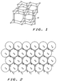
- Diamond-like lattice structure 10, illustrated in FIG. 1, is very interesting because the (111) plane in this structure is the same as the basal plane of a hexagonal closely packed (hcp) structure.
- hcp hexagonal closely packed
- FIG. 2 if a (111) layer (atoms designated A) is provided and a second similar layer (atoms designated B) is arranged on top, the structure is indistinct from the hcp. That is, the structure could be face centered cubic or hexagonal closely packed.
- a third layer atoms designated C
- a decision between an hcp and an fcc structure must be made.
- the structure is an hcp structure, or graphite.
- the layers of such a structure can be described as an ABABABAB structure. If the third layer is placed in a second possible location, displaced from both the A and B atoms in the X, Y and Z directions (see FIG. 2), the structure becomes an fcc structure, or diamond.
- the layers of FIG. 2 can be described as an ABCABCABC structure. In both structures (graphite and the diamond of FIGS. 2) the number of nearest neighbors is four.
- Graphite is effectively a metallic conductor with a conductivity of 1375 x 10 ⁇ 6ohm-cm. This is a difference of at least 7 orders of magnitude and as great as 20 orders of magnitude for the intrinsic properties.
- Graphite is a semi-metal with about 5 x 10¹⁸ carriers per cm3. Electrical conductivity of graphite is much greater in directions parallel to the hexagonal planes and low in the perpendicular direction (c-axis). The different orientations of the covalent bonds with their attendantly different energy levels act as efficient electrical conduction paths. Thus, there are great differences in electrical properties for very small changes in the crystal structure between graphite and diamond.
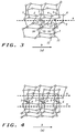
- a first defect is the screw dislocation, two embodiments of which are illustrated in FIGS. 3 and 4. There are also 60° dislocations that may easily form extended networks, and many other dislocations and variations.
- the (001) plane is the most important slip plane, and indeed, it appears that this is the only slip plane that occurs under any but the most playful circumstances.
- the shortest transitional distance between any two carbon atoms in the diamond lattice is along the ⁇ 110 ⁇ direction (specifically, ⁇ 1/2, 1/2, 0 ⁇ , that is along half the diagonal of a cubic face).
- Dislocations with Burgers vectors in the ⁇ 110 ⁇ direction are the most stable (lowest free energy). Any arbitrary direction in this lattice can be considered as the sum of successive ⁇ 110 ⁇ directions, and simple dislocations will have these same directions for their axes.
- the three types of simple dislocations having both their Burgers vectors and axes along the ⁇ 110 ⁇ direction are the screw dislocation, the 60° dislocation (with its Burgers vector 60° to the dislocation axis) and an edge type dislocation with a (100) glide plane. All of these dislocations are useful as electrically active defects.
- a screw defect is generally the result of shear, which occurs during the growth or deposition process of the diamond material.
- This dislocation like others, creates an elastic strain field in the surrounding crystal.
- G shear modulus.
- the strain energy of annulus 20 per unit length is The strain energy of the diamond crystal per unit dislocation length is where Ro and R are the lower and upper limits.
- Ro is the lower limit for this integration, that is, the level below which Hooke's law is not valid and the material behaves atomically.
- the value for Ro is not critical because the energy is a logarithmic function thereof.
- Upper level R is the boundary of the crystal or the point at which other dislocations cancel out the stress field. It should be noted that since the energy of the strain field created by the dislocation is a function of the square of the Burgers vector b , the crystal minimizes its free energy by dividing multiple dislocations into unit dislocations.
- the maximum radius of the strain, R is selected arbitrarily as 1uM. The actual maximum radius might be as far as the boundaries of the crystal. In reality, the range of the strain field from a crystal defect is typically as far as the distance to another defect that cancels out the strain field with its own strain field.
- the energy of the strain field is comparatively insensitive to both R and Ro.
- the energy varies as the logarithm of the ratio of the maximum field radius and minimum field radius (before the material behaves atomically).
- This example using the above numbers is a reasonable calculation of the magnitude of the energy to be used for estimating the possible behavior of the lattice.
- the strain energy becomes 17.8eV/ ⁇ , or 44.4eV per bond length. This is clearly enough energy to break the covalent bond of the diamond lattice and to allow local reconfiguration. It is possible to have both single bonds and even double bonds broken and reformed. By reconfiguring the bonds into covalent bonds remaining in a plane, a monolayer of graphite-like material is formed, along with its electrical properties. This thin film of graphitic structure then lends its properties to that of the diamond and an electrically active defect is formed.
- FIG. 6 a layer 30 of diamond-like material having an electrically active defect 32 is illustrated.
- defect 32 in layer 30 operates similar to an electron emitter formed of a sharp tip (10 angstrom radius) of a metallic conductor with a thin (10's of angstroms) diamond coating.
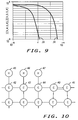
- FIGS. 7 - 9 are graphs illustrating electron emission properties of a prior art field emission device, such as the tip commonly referred to as a Spindt emitter, and the device of FIG. 6, respectively.
- FIG. 7 is a graph of emitted current, I, vs. voltage, or the field potential, applied to the tip.
- FIG. 7 a typical prior art tip with a radius of 200 ⁇ and a work function of the material of 4.5eV is utilized.
- the emitter of FIG. 6 operates like an emitter tip having a radius of 10 ⁇ and a work function of the material of 0.2eV.
- the electron emission is substantially greater for the emitter of FIG. 6 with a substantially smaller voltage, or field potential, applied.
- FIG. 9 is a graph comparing electron emission of the surface defect described above (curve 36), to a prior art field emission device (curve 35). Curves 35 and 36 depict electron emission for a free standing rod in an electric field as a function of tip radius, wherein a molybdenum rod with a work function of 4.5eV is used for curve 35 and the above described surface defect with a work function of 0.5eV is used for curve 36.
- the advantage of the lower work function of the surface defect is slowly lost to the sharp tip. If the standing rod is sharp enough, its work function approaches unimportance. Low work function is still desirable, but it becomes less necessary for enhanced emission as the emitter diameter shrinks. Since the defect described above (i.e., at the surface of the diamond) appears sharper than virtually any prior art field emitter tip, it has a substantial advantage in both work function and radius.
- a double bond has formed between carbon atoms 40 and 41 which is stronger than the surrounding single bonds and, thus, draws carbon atoms 40 and 41 slightly closer together.
- the low energy structure formed by carbon atoms 40 and 41 is a poor electron emitter and is undesirable in devices that require this property from the diamond.
- Carbon atoms 42, 43 and 44 have been hydrogenated, that is an atom of hydrogen 45, 46 and 47, respectively, is attached by a single bond.
- the lattice structure formed by carbon atoms 42, 43 and 44 appears the same at the surface and, therefore, appears as an extension of the bulk. Since the lattice structure of carbon atoms 42, 43 and 44 is an extension of the bulk it has the properties of the bulk and, therefore, is a good electron emitter.
- FIG. 11 illustrates a cross-sectional representation of a field emission device 50 employing a hydrogenated layer 52 of diamond-like carbon with electrically active defects 53, 54 and 55.
- the hydrogenation of layer 52 is illustrated by a layer 56 on the surface thereof.
- Electrically active defects 53, 54 and 55 appear generally periodically spaced and substantially perpendicular to the surface although it should be understood that some angular changes and some differences in spacing may occur. It is believed, for example, that the elongated defects should be positioned at an angle to the surface of the diamond-like carbon layer for best results. Further, it is believed that it is best if the elongated defect makes an angle in the range of 45° to 90° with the surface.
- Device 50 further includes a supporting substrate 57 having a conductive layer 58 formed on a surface thereof.
- Conductive layer 58, or layers, provide the means to electrically communicate with defects 53, 54 and 55.
- electrical current flows in conductive layer 58 from a source (not shown) and is emitted by defects 53, 54 and 55 into the free space above layer 56.
- Dislocations There are many possible kinds of lattice imperfections; vacancies, interstitials, impurities, dislocations, cellular and lineage substructure, grain boundaries, and surfaces. Vacancies in a lattice can actually lower the free energy of a crystal and are therefore present at equilibrium. Dislocations, which are of greater interest, do not lower the free energy of a crystal but instead raise it. Dislocations , therefore, are a nonequilibrium type of defect and, generally, can be formed only as a result of nonequilibrium conditions during growth of the crystal. There are several types of disturbances that can be effective in producing dislocations.
- a diamond-like carbon electron emitter with improved current characteristics including improved saturation current
- the improved current characteristics are realized through the incorporation of an electrically active defect which locally enhances electron emission.
- the defect is formed of the same basic material with a different structure.
- a field emission device with a diamond-like emitter, having improved current characteristics is disclosed. It should be noted that while carbon has been described throughout this disclosure, electron emitters incorporating other materials, such as aluminum nitride, might be enhanced in a similar fashion, i.e.,by including an electrically active defect.
Applications Claiming Priority (2)
| Application Number | Priority Date | Filing Date | Title |
|---|---|---|---|
| US08/011,595 US5619092A (en) | 1993-02-01 | 1993-02-01 | Enhanced electron emitter |
| US11595 | 1993-02-01 |
Publications (2)
| Publication Number | Publication Date |
|---|---|
| EP0609532A1 true EP0609532A1 (fr) | 1994-08-10 |
| EP0609532B1 EP0609532B1 (fr) | 1998-08-26 |
Family
ID=21751109
Family Applications (1)
| Application Number | Title | Priority Date | Filing Date |
|---|---|---|---|
| EP93120277A Expired - Lifetime EP0609532B1 (fr) | 1993-02-01 | 1993-12-16 | Emetteur d'électrons |
Country Status (7)
| Country | Link |
|---|---|
| US (4) | US5619092A (fr) |
| EP (1) | EP0609532B1 (fr) |
| JP (1) | JP3171290B2 (fr) |
| CN (1) | CN1059050C (fr) |
| DE (1) | DE69320617T2 (fr) |
| RU (1) | RU94011577A (fr) |
| TW (1) | TW232076B (fr) |
Cited By (20)
| Publication number | Priority date | Publication date | Assignee | Title |
|---|---|---|---|---|
| WO1995022168A1 (fr) * | 1994-02-14 | 1995-08-17 | The Regents Of The University Of California | Emetteur de champ diamant-graphite |
| WO1995022169A1 (fr) * | 1994-02-14 | 1995-08-17 | E.I. Du Pont De Nemours And Company | Emetteurs de champ en fibres de diamant |
| EP0701265A1 (fr) * | 1994-08-29 | 1996-03-13 | Canon Kabushiki Kaisha | Dispositif émetteur d'électrons, source d'électrons et appareil de formation d'images ainsi qu'un procédé pour leur fabrication |
| EP0705915A1 (fr) | 1994-10-03 | 1996-04-10 | Motorola, Inc. | Film émetteur d'électrons |
| EP0709870A1 (fr) * | 1994-10-31 | 1996-05-01 | AT&T Corp. | Procédé et appareil pour la fabrication d'émetteurs à effet de champ améliorés formés de particules, et produits ainsi obtenus |
| EP0709869A1 (fr) * | 1994-10-31 | 1996-05-01 | AT&T Corp. | Dispositifs à émission de champ utilisant des émetteurs à effet de champ améliorés en diamant |
| EP0730780A4 (fr) * | 1993-06-02 | 1996-07-22 | Microelectronics And Comp Tech | Cathode plate a emission de champ pourvue d'une pellicule de diamant amorphe |
| EP0727057A1 (fr) * | 1993-11-04 | 1996-08-21 | Microelectronics and Computer Technology Corporation | Procedes de fabrication de systemes et composants d'affichage a ecran plat |
| WO1997007522A1 (fr) * | 1995-08-14 | 1997-02-27 | Sandia Corporation | Procede de creation de sites d'emission par effet de champ controles |
| EP0764965A2 (fr) * | 1995-09-19 | 1997-03-26 | AT&T Corp. | Afficheurs à plasma utilisant des matériaux d'électrode à basse affinité électronique |
| EP0836217A1 (fr) * | 1996-10-14 | 1998-04-15 | Hamamatsu Photonics K.K. | Tube électronique |
| EP0841677A1 (fr) * | 1996-03-27 | 1998-05-13 | Matsushita Electric Industrial Co., Ltd. | Dispositif emetteur d'electrons et procede de fabrication |
| EP0924737A1 (fr) * | 1997-12-20 | 1999-06-23 | Philips Patentverwaltung GmbH | Matrice d'électrodes contenant de diamant et d'hydrogène |
| US6020677A (en) * | 1996-11-13 | 2000-02-01 | E. I. Du Pont De Nemours And Company | Carbon cone and carbon whisker field emitters |
| EP1004132A1 (fr) * | 1997-08-13 | 2000-05-31 | SI Diamond Technology, Inc. | Film de carbone pour dispositif a emission de champ |
| US6097139A (en) * | 1995-08-04 | 2000-08-01 | Printable Field Emitters Limited | Field electron emission materials and devices |
| AU728397B2 (en) * | 1994-08-29 | 2001-01-11 | Canon Kabushiki Kaisha | Electron-emitting device, electron source and image-forming apparatus as well as method of manufacturing the same |
| WO2001052296A1 (fr) * | 2000-01-14 | 2001-07-19 | Thomson Tubes Electroniques | Cathode generatrice d"electrons et son procede de fabrication |
| DE19910156C2 (de) * | 1999-02-26 | 2002-07-18 | Hahn Meitner Inst Berlin Gmbh | Elektronenemitter und Verfahren zu dessen Herstellung |
| US6992428B2 (en) | 2001-12-25 | 2006-01-31 | Canon Kabushiki Kaisha | Electron emitting device, electron source and image display device and methods of manufacturing these devices |
Families Citing this family (22)
| Publication number | Priority date | Publication date | Assignee | Title |
|---|---|---|---|---|
| US5619092A (en) * | 1993-02-01 | 1997-04-08 | Motorola | Enhanced electron emitter |
| JP3580930B2 (ja) * | 1996-01-18 | 2004-10-27 | 住友電気工業株式会社 | 電子放出装置 |
| US5973452A (en) * | 1996-11-01 | 1999-10-26 | Si Diamond Technology, Inc. | Display |
| WO1998045868A1 (fr) * | 1997-04-09 | 1998-10-15 | Matsushita Electric Industrial Co., Ltd. | Dispositif emetteur d'electrons et procede de fabrication associe |
| US6635979B1 (en) | 1998-02-09 | 2003-10-21 | Matsushita Electric Industrial Co., Ltd. | Electron emitting device, method of producing the same, and method of driving the same; and image display comprising the electron emitting device and method of producing the same |
| FR2780808B1 (fr) * | 1998-07-03 | 2001-08-10 | Thomson Csf | Dispositif a emission de champ et procedes de fabrication |
| US6181055B1 (en) | 1998-10-12 | 2001-01-30 | Extreme Devices, Inc. | Multilayer carbon-based field emission electron device for high current density applications |
| US6441550B1 (en) | 1998-10-12 | 2002-08-27 | Extreme Devices Inc. | Carbon-based field emission electron device for high current density applications |
| KR100311209B1 (ko) * | 1998-10-29 | 2001-12-17 | 박종섭 | 전계방출표시소자의제조방법 |
| US6059627A (en) * | 1999-03-08 | 2000-05-09 | Motorola, Inc. | Method of providing uniform emission current |
| RU2155412C1 (ru) * | 1999-07-13 | 2000-08-27 | Закрытое акционерное общество "Патинор Коутингс Лимитед" | Плоский люминесцентный экран, способ изготовления плоского люминесцентного экрана и способ получения изображения на плоском люминесцентном экране |
| DE10036889C1 (de) * | 2000-07-28 | 2002-04-18 | Infineon Technologies Ag | Verfahren und Einrichtung zur Bestimmung eines in einem differentiellen Sendesignalabschnitt eines Funkgerätes auftretenden Offsetwerts |
| US6686696B2 (en) * | 2001-03-08 | 2004-02-03 | Genvac Aerospace Corporation | Magnetron with diamond coated cathode |
| US6554673B2 (en) | 2001-07-31 | 2003-04-29 | The United States Of America As Represented By The Secretary Of The Navy | Method of making electron emitters |
| US6847045B2 (en) | 2001-10-12 | 2005-01-25 | Hewlett-Packard Development Company, L.P. | High-current avalanche-tunneling and injection-tunneling semiconductor-dielectric-metal stable cold emitter, which emulates the negative electron affinity mechanism of emission |
| US6822380B2 (en) | 2001-10-12 | 2004-11-23 | Hewlett-Packard Development Company, L.P. | Field-enhanced MIS/MIM electron emitters |
| US6577058B2 (en) | 2001-10-12 | 2003-06-10 | Hewlett-Packard Development Company, L.P. | Injection cold emitter with negative electron affinity based on wide-gap semiconductor structure with controlling base |
| EP1826796A4 (fr) * | 2003-07-11 | 2008-04-02 | Tetranova Ltd | Cathodes a froid en materiaux a base de carbone |
| US7327829B2 (en) * | 2004-04-20 | 2008-02-05 | Varian Medical Systems Technologies, Inc. | Cathode assembly |
| TWI324024B (en) * | 2005-01-14 | 2010-04-21 | Hon Hai Prec Ind Co Ltd | Field emission type light source |
| GB0620259D0 (en) * | 2006-10-12 | 2006-11-22 | Astex Therapeutics Ltd | Pharmaceutical compounds |
| JP5450022B2 (ja) * | 2009-12-11 | 2014-03-26 | 株式会社デンソー | 熱電子発電素子 |
Citations (1)
| Publication number | Priority date | Publication date | Assignee | Title |
|---|---|---|---|---|
| JPH05135687A (ja) * | 1991-03-08 | 1993-06-01 | Canon Inc | 半導体電子放出素子 |
Family Cites Families (10)
| Publication number | Priority date | Publication date | Assignee | Title |
|---|---|---|---|---|
| US3921022A (en) * | 1974-09-03 | 1975-11-18 | Rca Corp | Field emitting device and method of making same |
| EP0713241B1 (fr) * | 1987-02-06 | 2001-09-19 | Canon Kabushiki Kaisha | Dispositif d'affichage comprenant un élément émetteur d'électrons |
| GB8818445D0 (en) * | 1988-08-03 | 1988-09-07 | Jones B L | Stm probe |
| NL8802409A (nl) * | 1988-09-30 | 1990-04-17 | Philips Nv | Weergeefinrichting, steunplaat voorzien van diode en geschikt voor de weergeefinrichting en werkwijze ter vervaardiging van de steunplaat. |
| US5141460A (en) * | 1991-08-20 | 1992-08-25 | Jaskie James E | Method of making a field emission electron source employing a diamond coating |
| US5129850A (en) * | 1991-08-20 | 1992-07-14 | Motorola, Inc. | Method of making a molded field emission electron emitter employing a diamond coating |
| US5536193A (en) * | 1991-11-07 | 1996-07-16 | Microelectronics And Computer Technology Corporation | Method of making wide band gap field emitter |
| US5686791A (en) * | 1992-03-16 | 1997-11-11 | Microelectronics And Computer Technology Corp. | Amorphic diamond film flat field emission cathode |
| US5449970A (en) * | 1992-03-16 | 1995-09-12 | Microelectronics And Computer Technology Corporation | Diode structure flat panel display |
| US5619092A (en) * | 1993-02-01 | 1997-04-08 | Motorola | Enhanced electron emitter |
-
1993
- 1993-02-01 US US08/011,595 patent/US5619092A/en not_active Expired - Fee Related
- 1993-11-10 TW TW082109441A patent/TW232076B/zh active
- 1993-12-16 DE DE69320617T patent/DE69320617T2/de not_active Expired - Fee Related
- 1993-12-16 EP EP93120277A patent/EP0609532B1/fr not_active Expired - Lifetime
-
1994
- 1994-01-25 JP JP2305194A patent/JP3171290B2/ja not_active Expired - Fee Related
- 1994-01-25 CN CN94101129A patent/CN1059050C/zh not_active Expired - Fee Related
- 1994-04-08 RU RU94011577A patent/RU94011577A/ru unknown
-
1996
- 1996-03-19 US US08/618,484 patent/US5753997A/en not_active Expired - Fee Related
- 1996-10-29 US US08/740,457 patent/US5757114A/en not_active Expired - Fee Related
-
1997
- 1997-08-25 US US08/917,123 patent/US5945778A/en not_active Expired - Fee Related
Patent Citations (1)
| Publication number | Priority date | Publication date | Assignee | Title |
|---|---|---|---|---|
| JPH05135687A (ja) * | 1991-03-08 | 1993-06-01 | Canon Inc | 半導体電子放出素子 |
Non-Patent Citations (2)
| Title |
|---|
| C.WANG ET AL: "Cold Field Emission From CVD Diamond Films Observed In Emission Electron Microscopy", ELECTRONICS LETTERS, vol. 27, no. 16, 1 August 1991 (1991-08-01), STEVENAGE, HERTS, UK, pages 1459 - 1461, XP000259873 * |
| PATENT ABSTRACTS OF JAPAN vol. 17, no. 511 (E - 1432) 14 September 1993 (1993-09-14) * |
Cited By (40)
| Publication number | Priority date | Publication date | Assignee | Title |
|---|---|---|---|---|
| EP0730780A1 (fr) * | 1993-06-02 | 1996-09-11 | Microelectronics and Computer Technology Corporation | Cathode plate a emission de champ pourvue d'une pellicule de diamant amorphe |
| EP0730780A4 (fr) * | 1993-06-02 | 1996-07-22 | Microelectronics And Comp Tech | Cathode plate a emission de champ pourvue d'une pellicule de diamant amorphe |
| EP0727057A4 (fr) * | 1993-11-04 | 1997-08-13 | Microelectronics & Computer | Procedes de fabrication de systemes et composants d'affichage a ecran plat |
| EP0727057A1 (fr) * | 1993-11-04 | 1996-08-21 | Microelectronics and Computer Technology Corporation | Procedes de fabrication de systemes et composants d'affichage a ecran plat |
| WO1995022169A1 (fr) * | 1994-02-14 | 1995-08-17 | E.I. Du Pont De Nemours And Company | Emetteurs de champ en fibres de diamant |
| WO1995022168A1 (fr) * | 1994-02-14 | 1995-08-17 | The Regents Of The University Of California | Emetteur de champ diamant-graphite |
| US5602439A (en) * | 1994-02-14 | 1997-02-11 | The Regents Of The University Of California, Office Of Technology Transfer | Diamond-graphite field emitters |
| US5578901A (en) * | 1994-02-14 | 1996-11-26 | E. I. Du Pont De Nemours And Company | Diamond fiber field emitters |
| AU708413B2 (en) * | 1994-08-29 | 1999-08-05 | Canon Kabushiki Kaisha | Electron-emitting device, electron source and image-forming apparatus as well as method of manufacturing the same |
| US6608437B1 (en) | 1994-08-29 | 2003-08-19 | Canon Kabushiki Kaisha | Electron-emitting device, electron source and image-forming apparatus as well as method of manufacturing the same |
| AU728397B2 (en) * | 1994-08-29 | 2001-01-11 | Canon Kabushiki Kaisha | Electron-emitting device, electron source and image-forming apparatus as well as method of manufacturing the same |
| US6179678B1 (en) | 1994-08-29 | 2001-01-30 | Canon Kabushiki Kaisha | Method of manufacturing electron-emitting device electron source and image-forming apparatus |
| US7758762B2 (en) | 1994-08-29 | 2010-07-20 | Canon Kabushiki Kaisha | Method for manufacturing an electron-emitting device with first and second carbon films |
| US6246168B1 (en) | 1994-08-29 | 2001-06-12 | Canon Kabushiki Kaisha | Electron-emitting device, electron source and image-forming apparatus as well as method of manufacturing the same |
| CN1056013C (zh) * | 1994-08-29 | 2000-08-30 | 佳能株式会社 | 电子发射器件、电子源和图象形成装置 |
| EP0701265A1 (fr) * | 1994-08-29 | 1996-03-13 | Canon Kabushiki Kaisha | Dispositif émetteur d'électrons, source d'électrons et appareil de formation d'images ainsi qu'un procédé pour leur fabrication |
| EP0915493B1 (fr) * | 1994-08-29 | 2003-10-22 | Canon Kabushiki Kaisha | Procédé pour la fabrication d'un dispositif émetteur d'électrons, |
| US7234985B2 (en) | 1994-08-29 | 2007-06-26 | Canon Kabushiki Kaisha | Method for manufacturing an electric emitting device with first and second carbon films |
| US7057336B2 (en) | 1994-08-29 | 2006-06-06 | Canon Kabushiki Kaisha | Electron-emitting device, electron source and image-forming apparatus as well as method of manufacturing the same |
| EP0705915A1 (fr) | 1994-10-03 | 1996-04-10 | Motorola, Inc. | Film émetteur d'électrons |
| EP0709869A1 (fr) * | 1994-10-31 | 1996-05-01 | AT&T Corp. | Dispositifs à émission de champ utilisant des émetteurs à effet de champ améliorés en diamant |
| US5637950A (en) * | 1994-10-31 | 1997-06-10 | Lucent Technologies Inc. | Field emission devices employing enhanced diamond field emitters |
| US5623180A (en) * | 1994-10-31 | 1997-04-22 | Lucent Technologies Inc. | Electron field emitters comprising particles cooled with low voltage emitting material |
| EP0709870A1 (fr) * | 1994-10-31 | 1996-05-01 | AT&T Corp. | Procédé et appareil pour la fabrication d'émetteurs à effet de champ améliorés formés de particules, et produits ainsi obtenus |
| US6097139A (en) * | 1995-08-04 | 2000-08-01 | Printable Field Emitters Limited | Field electron emission materials and devices |
| WO1997007522A1 (fr) * | 1995-08-14 | 1997-02-27 | Sandia Corporation | Procede de creation de sites d'emission par effet de champ controles |
| EP0764965A3 (fr) * | 1995-09-19 | 1998-01-28 | AT&T Corp. | Afficheurs à plasma utilisant des matériaux d'électrode à basse affinité électronique |
| EP0764965A2 (fr) * | 1995-09-19 | 1997-03-26 | AT&T Corp. | Afficheurs à plasma utilisant des matériaux d'électrode à basse affinité électronique |
| EP0841677A1 (fr) * | 1996-03-27 | 1998-05-13 | Matsushita Electric Industrial Co., Ltd. | Dispositif emetteur d'electrons et procede de fabrication |
| EP0841677A4 (fr) * | 1996-03-27 | 2000-03-08 | Matsushita Electric Ind Co Ltd | Dispositif emetteur d'electrons et procede de fabrication |
| EP0836217A1 (fr) * | 1996-10-14 | 1998-04-15 | Hamamatsu Photonics K.K. | Tube électronique |
| US5959400A (en) * | 1996-10-14 | 1999-09-28 | Hamamatsu Photonics K.K. | Electron tube having a diamond field emitter |
| US6020677A (en) * | 1996-11-13 | 2000-02-01 | E. I. Du Pont De Nemours And Company | Carbon cone and carbon whisker field emitters |
| EP1004132A1 (fr) * | 1997-08-13 | 2000-05-31 | SI Diamond Technology, Inc. | Film de carbone pour dispositif a emission de champ |
| EP1004132A4 (fr) * | 1997-08-13 | 2000-11-08 | Si Diamond Techn Inc | Film de carbone pour dispositif a emission de champ |
| EP0924737A1 (fr) * | 1997-12-20 | 1999-06-23 | Philips Patentverwaltung GmbH | Matrice d'électrodes contenant de diamant et d'hydrogène |
| DE19910156C2 (de) * | 1999-02-26 | 2002-07-18 | Hahn Meitner Inst Berlin Gmbh | Elektronenemitter und Verfahren zu dessen Herstellung |
| FR2803944A1 (fr) * | 2000-01-14 | 2001-07-20 | Thomson Tubes Electroniques | Cathode generatrice d'electrons et son procede de fabrication |
| WO2001052296A1 (fr) * | 2000-01-14 | 2001-07-19 | Thomson Tubes Electroniques | Cathode generatrice d"electrons et son procede de fabrication |
| US6992428B2 (en) | 2001-12-25 | 2006-01-31 | Canon Kabushiki Kaisha | Electron emitting device, electron source and image display device and methods of manufacturing these devices |
Also Published As
| Publication number | Publication date |
|---|---|
| JP3171290B2 (ja) | 2001-05-28 |
| US5619092A (en) | 1997-04-08 |
| CN1092904A (zh) | 1994-09-28 |
| CN1059050C (zh) | 2000-11-29 |
| JPH06318428A (ja) | 1994-11-15 |
| DE69320617D1 (de) | 1998-10-01 |
| US5945778A (en) | 1999-08-31 |
| TW232076B (fr) | 1994-10-11 |
| RU94011577A (ru) | 1995-12-10 |
| DE69320617T2 (de) | 1999-03-11 |
| US5753997A (en) | 1998-05-19 |
| EP0609532B1 (fr) | 1998-08-26 |
| US5757114A (en) | 1998-05-26 |
Similar Documents
| Publication | Publication Date | Title |
|---|---|---|
| EP0609532B1 (fr) | Emetteur d'électrons | |
| EP0555076B1 (fr) | Source d'électrons avec couche de diamant polycrystalline | |
| US5825122A (en) | Field emission cathode and a device based thereon | |
| Landheer et al. | Tunneling through AlAs barriers: Γ–X transfer current | |
| Geis et al. | A new surface electron-emission mechanism in diamond cathodes | |
| US5608283A (en) | Electron-emitting devices utilizing electron-emissive particles which typically contain carbon | |
| EP0601692B1 (fr) | Dispositif électronique avec un super-réseau artificiel | |
| US6204595B1 (en) | Amorphous-diamond electron emitter | |
| US5211707A (en) | Semiconductor metal composite field emission cathodes | |
| Silva et al. | Modeling of the electron field emission process in polycrystalline diamond and diamond-like carbon thin films | |
| US6891324B2 (en) | Carbon-metal nano-composite materials for field emission cathodes and devices | |
| US6084340A (en) | Electron emitter with nano-crystalline diamond having a Raman spectrum with three lines | |
| Givargizov et al. | Field emission characteristics of polycrystalline and single-crystalline diamond grown on Si tips | |
| Lee et al. | Electron field emission characteristics of planar diamond film array synthesized by chemical vapor deposition process | |
| Tondare et al. | Self-assembled Ge nanostructures as field emitters | |
| Krauss et al. | Morphology and electron emission properties of nanocrystalline CVD diamond thin films | |
| Ohno et al. | Field-ion microscopy of GaAs and GaP | |
| Chung et al. | Band structure calculation of field emission from Al x Ga 1− x N as a function of stoichiometry | |
| KR100216695B1 (ko) | 개선된 전자 방출기 | |
| US6870309B2 (en) | Cold emission film cathode and flat panel display with nanocrystalline carbon film emitter | |
| HIRAKI et al. | Field emission from multilayered carbon films consisting of nano seeded diamond and nanocluster carbon, deposited at room-temperature on glass substrates | |
| Zakhidov et al. | Statistical analysis of low-voltage electron emission from nanocarbon cathodes | |
| Jung et al. | Effect of N doping on the electron emission properties of diamondlike carbon film on a 2-in. Mo field emitter array panel | |
| KR100324082B1 (ko) | 전계 방출팁 | |
| Gomez‐Yanez et al. | Structural and electrical characterization of gold/chemically vapor deposited diamond contact |
Legal Events
| Date | Code | Title | Description |
|---|---|---|---|
| PUAI | Public reference made under article 153(3) epc to a published international application that has entered the european phase |
Free format text: ORIGINAL CODE: 0009012 |
|
| AK | Designated contracting states |
Kind code of ref document: A1 Designated state(s): DE FR GB |
|
| 17P | Request for examination filed |
Effective date: 19950210 |
|
| 17Q | First examination report despatched |
Effective date: 19951204 |
|
| GRAG | Despatch of communication of intention to grant |
Free format text: ORIGINAL CODE: EPIDOS AGRA |
|
| GRAG | Despatch of communication of intention to grant |
Free format text: ORIGINAL CODE: EPIDOS AGRA |
|
| GRAH | Despatch of communication of intention to grant a patent |
Free format text: ORIGINAL CODE: EPIDOS IGRA |
|
| GRAH | Despatch of communication of intention to grant a patent |
Free format text: ORIGINAL CODE: EPIDOS IGRA |
|
| GRAA | (expected) grant |
Free format text: ORIGINAL CODE: 0009210 |
|
| AK | Designated contracting states |
Kind code of ref document: B1 Designated state(s): DE FR GB |
|
| REF | Corresponds to: |
Ref document number: 69320617 Country of ref document: DE Date of ref document: 19981001 |
|
| ET | Fr: translation filed | ||
| PLBE | No opposition filed within time limit |
Free format text: ORIGINAL CODE: 0009261 |
|
| STAA | Information on the status of an ep patent application or granted ep patent |
Free format text: STATUS: NO OPPOSITION FILED WITHIN TIME LIMIT |
|
| 26N | No opposition filed | ||
| PGFP | Annual fee paid to national office [announced via postgrant information from national office to epo] |
Ref country code: GB Payment date: 19991001 Year of fee payment: 7 |
|
| PGFP | Annual fee paid to national office [announced via postgrant information from national office to epo] |
Ref country code: DE Payment date: 19991021 Year of fee payment: 7 |
|
| PGFP | Annual fee paid to national office [announced via postgrant information from national office to epo] |
Ref country code: FR Payment date: 19991202 Year of fee payment: 7 |
|
| PG25 | Lapsed in a contracting state [announced via postgrant information from national office to epo] |
Ref country code: GB Free format text: LAPSE BECAUSE OF NON-PAYMENT OF DUE FEES Effective date: 20001216 |
|
| GBPC | Gb: european patent ceased through non-payment of renewal fee |
Effective date: 20001216 |
|
| PG25 | Lapsed in a contracting state [announced via postgrant information from national office to epo] |
Ref country code: FR Free format text: LAPSE BECAUSE OF NON-PAYMENT OF DUE FEES Effective date: 20010831 |
|
| REG | Reference to a national code |
Ref country code: FR Ref legal event code: ST |
|
| PG25 | Lapsed in a contracting state [announced via postgrant information from national office to epo] |
Ref country code: DE Free format text: LAPSE BECAUSE OF NON-PAYMENT OF DUE FEES Effective date: 20011002 |