EP0603867B1 - Circuit de compensation de distorsion d'amplificateur de puissance à haute fréquence - Google Patents
Circuit de compensation de distorsion d'amplificateur de puissance à haute fréquence Download PDFInfo
- Publication number
- EP0603867B1 EP0603867B1 EP93120728A EP93120728A EP0603867B1 EP 0603867 B1 EP0603867 B1 EP 0603867B1 EP 93120728 A EP93120728 A EP 93120728A EP 93120728 A EP93120728 A EP 93120728A EP 0603867 B1 EP0603867 B1 EP 0603867B1
- Authority
- EP
- European Patent Office
- Prior art keywords
- circuit
- gain
- signal
- power amplifier
- frequency power
- Prior art date
- Legal status (The legal status is an assumption and is not a legal conclusion. Google has not performed a legal analysis and makes no representation as to the accuracy of the status listed.)
- Expired - Lifetime
Links
- 238000001514 detection method Methods 0.000 claims description 23
- 238000000034 method Methods 0.000 description 23
- 238000010586 diagram Methods 0.000 description 20
- 230000006866 deterioration Effects 0.000 description 5
- 230000005540 biological transmission Effects 0.000 description 3
- 238000005516 engineering process Methods 0.000 description 2
- 230000010355 oscillation Effects 0.000 description 2
- 239000003990 capacitor Substances 0.000 description 1
- 238000006243 chemical reaction Methods 0.000 description 1
- 238000010276 construction Methods 0.000 description 1
- 230000001419 dependent effect Effects 0.000 description 1
- 102220014334 rs397517040 Human genes 0.000 description 1
Images


Classifications
-
- H—ELECTRICITY
- H03—ELECTRONIC CIRCUITRY
- H03G—CONTROL OF AMPLIFICATION
- H03G3/00—Gain control in amplifiers or frequency changers
- H03G3/20—Automatic control
- H03G3/30—Automatic control in amplifiers having semiconductor devices
- H03G3/3036—Automatic control in amplifiers having semiconductor devices in high-frequency amplifiers or in frequency-changers
- H03G3/3042—Automatic control in amplifiers having semiconductor devices in high-frequency amplifiers or in frequency-changers in modulators, frequency-changers, transmitters or power amplifiers
-
- H—ELECTRICITY
- H03—ELECTRONIC CIRCUITRY
- H03F—AMPLIFIERS
- H03F1/00—Details of amplifiers with only discharge tubes, only semiconductor devices or only unspecified devices as amplifying elements
- H03F1/32—Modifications of amplifiers to reduce non-linear distortion
- H03F1/3241—Modifications of amplifiers to reduce non-linear distortion using predistortion circuits
- H03F1/3247—Modifications of amplifiers to reduce non-linear distortion using predistortion circuits using feedback acting on predistortion circuits
Definitions
- the present invention relates to a distortion compensating circuit of a high-frequency power amplifier of the kind used in transmitter apparatus and the like.
- the input/output characteristic of a power amplifier generally is a non-linear characteristic such as that shown in Fig. 1 by a solid line, this characteristic produces non-linear distortion (waveform distortion) dependent on the signal amplitude.
- this characteristic produces non-linear distortion (waveform distortion) dependent on the signal amplitude.
- the power source is a battery and low voltage operation is required, when driven at low voltages the non-linear characteristic becomes marked, and non-linear distortion readily occurs.
- Fig. 2 shows the distortion compensating circuit of the conventional negative feedback method.
- the input signal is supplied to the power amplifier 1 and to an envelope detecting circuit 2, and a detection signal showing the envelope waveform of the input signal is derived.
- the output signal of the amplifier 1 has been brought to the same level as the input signal by an attenuator circuit 3, it is supplied to an envelope detecting circuit 4, and a detection signal showing the envelope waveform of the output signal is derived.
- the detection signals of the detecting circuits 2 and 4 are supplied to a subtracting circuit 5 and the difference component between these signals, i.e. the non-linear distortion component, is detected, and for instance the power source voltage of the amplifier 1 is controlled based upon this distortion component, and the amplifier gain is thereby controlled.
- an output signal which has been power-amplified and compensated for non-linear distortion is derived from the amplifier 1.
- Fig. 3 shows the distortion compensating circuit of the predistorter method of the conventional technology.
- an input signal is supplied to a distortion forming circuit 6, and a distortion signal for canceling the non-linear distortion generated in the power amplifier 1 is produced.
- This distortion signal is added to the originally supplied input signal in an adding circuit 7, and thereafter is supplied to the power amplifier 1.
- Fig. 4 shows the distortion compensating circuit of the feed-forward method of the conventional technology.
- the differential component between the input signal of the amplifier 1 and the output signal thereof i.e. the non-linear distortion component
- This distortion component is amplified to the level of the non-linear distortion component contained in the output signal of the amplifier 1 by an amplifier 8, and is then supplied to a subtraction circuit 9, and the non-linear distortion component contained in the output signal of the amplifier 1 is removed.
- the distortion compensating characteristic hardly deteriorates at all; however, because the negative feedback method is a closed loop control method, when the linearity of the loop is not maintained, its operation can become unstable and oscillation can occur. Then, when the power source voltage and thereby the gain of the amplifier 1 is controlled based upon the distortion detection output from the subtraction circuit 5, the change in the gain of the amplifier 1 with respect to this detection output does not become linear. Therefore, with the negative feedback method, in order to avoid such oscillation and maintain stable operation, the loop gain must be kept low. As a result, the distortion compensating amount cannot be made large.
- the present invention aims to solve these problems.
- the non-linear distortion which occurs in the power amplifier 1 is caused by non-linearity of the input/output characteristic of the power amplifier 1. From a different point of view, it may be conceived that such non-linear distortion is caused by gain error of the power amplifier 1. Then, if it is gain error that causes the non-linear distortion, by detecting the gain error and correcting the level of the input signal based upon the detected gain error, the gain error can be canceled.
- This invention uses this approach to compensate for the non-linear distortion of a power amplifier.
- a variable gain circuit 12 provided at a front stage of the high-frequency power amplifier, for variable-controlling the level of an input signal S12 to be supplied to the high-frequency power amplifier 13; a gain detecting circuit 25 for detecting the gain of the high-frequency power amplifier 13; and a loop filter 28 for supplying the output signal S24 of this gain detecting circuit 25 to the variable gain circuit 12 as a control voltage thereof.
- the gain detecting circuit 25 is made up of: a first logarithm converting circuit 22 for logarithmically converting an envelope detection signal S21 of a signal S11 inputted into the variable gain circuit 12; a second logarithm converting circuit 23 for logarithmically converting an envelope detection signal S27 of an output signal S13 from the high-frequency power amplifier; and a subtraction circuit 24 for outputting a subtraction signal S24 of the respective output signals S22 and S23 of the first and second logarithm converting circuits 22 and 23.
- the control voltage vs. gain characteristic of the variable gain circuit 12 is an inverse logarithm characteristic.
- the non-linear distortion of the high-frequency power amplifier 13 is detected, and this detection signal S24 is negative-fed back to the variable-gain circuit 12, and the non-linear distortion is compensated.
- FIG. 5 A preferred embodiment of the present invention is illustrated in Fig. 5.
- the present invention has been applied to a transmitter circuit for a portable telephone in a digital cellular-phone system. That is, in Fig. 5, digital voice data "I" and "Q" of a base band which has been A/D-converted from a voice signal are supplied to a QPSK modulating circuit 11 and made into, for instance, a QPSK signal S11 in a 900 MHz band.
- This signal S11 is supplied to a variable gain amplifier 12 and made into a level-controlled signal S12, as will be further discussed later, and this signal S12 is supplied to a high-frequency power amplifier 13 for transmission use, power-amplified, and derived as a signal S13.
- control voltage vs. gain characteristic of the variable gain control amplifier 12 becomes an inverse logarithm characteristic (exponential characteristic), for example as shown in Fig. 6, and, as a result, as shown in Fig. 6B, the logarithmic value of the gain with respect to the control voltage becomes linear. It is noted that generally speaking, a variable control amplifier has this kind of control characteristic.
- the signal S11 from the modulating circuit 11 is also supplied to an envelope detecting circuit 21 and a detection signal S21 indicative of the envelope waveform of the signal S11 is derived, and this signal S21 is supplied to a logarithm amplifier 22 and converted into a signal S22 indicative of the logarithmic value of the signal S21.
- this first logarithm amplifier 22 and a second logarithm amplifier 23 and a subtraction circuit 24 constitute a gain detecting circuit 25.
- the signal S13 from the power amplifier 13 is supplied to an attenuator circuit 26 and made into a signal S13 having a level equal to that of the signal S11.
- This signal S13 is supplied to an envelope detecting circuit 27, and a detection signal S27 showing the envelope waveform of the signal S13 is derived.
- This signal S27 is supplied to the logarithm amplifier 23 and converted into a signal S23 indicative of the logarithmic value of the signal S27.
- the logarithm amplifiers 22 and 23 may be constructed by utilizing the voltage vs. current characteristic of a PN junction.
- the loop filter 28 may be constructed from a mirror integrating circuit in which a resistor 28R and a capacitor 28C are connected to an operational amplifier 28A.
- the level of the input signal S11 (the envelope detection signal S21) is divided by the level of the output signal S13 (the envelope detection signal S27), and the logarithmic value S24 of the quotient (S21/S27) is outputted.
- the gain G12 of the variable gain amplifier 12 varies in a linear fashion in proportion to the quotient (S21/S27) between the level of the input signal S12 (envelope detection signal S21) and the level of the output signal S11 (envelope detection signal S27). Therefore, in the example shown in Fig. 5, as a result of the variable gain amplifier 12 being controlled by the gain detection circuit 25, the negative feedback control system becomes linear.
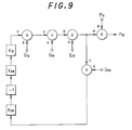
- Fig. 8 is a block diagram showing the circuit described above.
- the transfer functions of the envelope detecting circuits 21 and 27 are 1. Also,
- FIG. 10 the block diagram of this figure 8 becomes the block diagram of Fig. 9 by equivalent conversion. Furthermore, this block diagram may be rewritten as shown in Figs. 10A to 10C.
- the total gain (P13-P11) [dB] of the amplifiers 12 and 13 is equal to the attenuation amount (G26) of the attenuator circuit 26.
- the attenuation amount of the attenuator circuit 26.
- Fig. 10C may be rewritten as shown in Fig. 10D by thinking of the non-linear distortion E13 of the power amplifier 13 as disturbance.
- G(s) K12 * K25 * K28
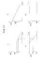
- Fig. 11A and Fig. 11B are obtained.
- the non-linear distortion occurring in the power amplifier 13 is caused by the gain error of the power amplifier 13, the gain error is detected, and the level of the signal S12 inputted to the power amplifier 13 is corrected based upon the detected output, even when the input/output characteristic of the power amplifier 13 is a non-linear characteristic, the non-linear distortion caused by this non-linear characteristic can be compensated.
- this compensating method corresponds to the negative feedback method in a broad sense
- the gain error of the power amplifier 13 is detected in a logarithmic value state, and the gain of the variable gain amplifier 12 having the inverse logarithm characteristic is controlled by this detection signal, as shown in Fig. 11
- the system becomes a linear control system. Accordingly, since a sufficient loop gain may be obtained, the distortion compensating characteristic hardly deteriorates at all with respect to the temperature characteristics and age deterioration, and this distortion compensation is reliably achieved. For instance, there is a circuit which produces a direct current offset within the negative feedback loop, and no adjustment of this direct current offset is required. Also, when either the power source voltage of the power amplifier 13 has been made low, or the power source voltage has changed, even if distortion happens to occur in the power amplifier 13, since this distortion is also compensated, the efficiency of the power amplifier 13 can be increased.
- Fig. 12 shows a second preferred embodiment of the present invention.
- the detection signals S21 and S27 are A/D-converted by A/D converters 31 and 32, a gain detecting circuit 25 and a loop filter 28 are made digital, and after the output signal of the filter 28 has been converted into an analog signal by a D/A converter 33, this analog signal is supplied to the variable gain amplifier 12 as a control voltage.
- Fig. 13 shows a third preferred embodiment of the present invention.
- base band digital voice data I and Q which are supplied to a QPSK modulating circuit 11 are supplied to an envelope forming circuit 34, and a digital signal S34 representative of the envelope waveform of the modulation signal S11 is formed.
- This signal S34 is supplied to a D/A converter 35 and an analog signal indicative of the envelope waveform of the modulation signal S11, namely a signal S21, is derived. Then, this signal S21 is supplied to a gain detecting circuit 25.
- a gain detecting circuit 25 As a result, distortion occurring in the amplifier 13 can be similarly compensated.
- Fig. 14 shows a fourth preferred embodiment of the present invention.
- Features in Fig. 14 which are the same as features in Fig. 5 have been given the same reference numerals, and their detailed description will be omitted here.
- the digital signal S34 representative of the envelope waveform of the modulation signal S11 is derived from the envelope forming circuit 34, both an A/D converter 32 and a D/A converter 33 are provided, as in the example of Fig. 12, and also both the gain detecting circuit 25 and the filter 28 are digital circuits, so that the distortion compensation is performed digitally.
- Fig. 15 shows a fifth preferred embodiment of the present invention.
- a variable attenuator circuit 36 is provided as the variable gain circuit instead of the variable gain amplifier 12.
- the output signal of the filter 28 is supplied as the control voltage to this variable attenuator circuit 36.
- the characteristic of the attenuation amount with respect to the control voltage of the variable attenuator circuit 36 is made an inverse logarithm characteristic similar to that of Fig. 6.
- the non-linear distortion occurring in the power amplifier 13 is caused by the gain errors of the power amplifier 13, and the gain errors are detected, and then the level of the signal S12 inputted to the power amplifier 13 is corrected based upon the detected output, even when the input/output characteristic of the power amplifier 13 is a non-linear characteristic, the non-linear distortion caused by this non-linear characteristic can be compensated.
- this compensating method corresponds to the negative feedback method in a broad sense
- the gain error of the power amplifier 13 is detected in a logarithmic value state, and the gain of the variable gain amplifier 12 having an inverse logarithm characteristic is controlled by this detection signal, the system as shown in Fig. 11 becomes the linear-control system. Accordingly, since a satisfactorily full loop gain may be obtained, the distortion compensating characteristic is not substantially changed with respect to the temperature characteristics and age deterioration, and this distortion compensation is achieved reliably. Also, when the power source voltage of the power amplifier 13 is set to a low voltage, or when the power source voltage has changed, even if distortion is produced in the power amplifier 13, since this distortion is also compensated, the efficiency of the power amplifier 13 can be increased.
Landscapes
- Physics & Mathematics (AREA)
- Nonlinear Science (AREA)
- Engineering & Computer Science (AREA)
- Power Engineering (AREA)
- Amplifiers (AREA)
- Tone Control, Compression And Expansion, Limiting Amplitude (AREA)
- Control Of Amplification And Gain Control (AREA)
Claims (5)
- Circuit de compensation de distorsion d'un amplificateur de puissance à haute fréquence, pour compenser la distorsion non linéaire de l'amplificateur de puissance à haute fréquence (13) par une réaction négative, comprenant :un circuit à gain variable (12), disposé au niveau d'un étage avant dudit amplificateur de puissance à haute fréquence (13), pour une commande variable du niveau d'un signal d'entrée à délivrer audit amplificateur de puissance à haute fréquence ;un circuit de détection de gain (25) pour détecter le gain dudit amplificateur de puissance à haute fréquence 13 ; etun filtre de boucle (28) pour délivrer le signal de sortie de ce circuit de détection de gain (25) audit circuit à gain variable (12) en tant que tension de commande de ce dernier ;dans lequel ledit circuit de détection de gain (25) comprend :un premier circuit de conversion logarithmique (22) pour transformer, de manière logarithmique, un signal de détection d'enveloppe du signal entré dans ledit circuit à gain variable ;un second circuit de conversion logarithmique (23) pour transformer, de manière logarithmique, un signal de détection d'enveloppe du signal de sortie en provenance dudit amplificateur de puissance à haute fréquence ; etun circuit de soustraction (24) pour sortir un signal de soustraction des signaux de sortie respectifs desdits premier et second circuits de conversion logarithmique (22, 23) ;et dans lequel la courbe de la tension de commande par rapport au gain dudit circuit à gain variable est une courbe logarithmique inverse.
- Circuit de compensation de distorsion d'un amplificateur de puissance à haute fréquence selon la revendication 1, dans lequel ledit circuit à gain variable (12) comprend un circuit amplificateur à gain variable.
- Circuit de compensation de distorsion d'un amplificateur de puissance à haute fréquence selon la revendication 1, dans lequel le signal de détection d'enveloppe délivré audit circuit de détection de gain (25) est un signal numérique ;ledit circuit de détection de gain (25) et ledit filtre de boucle (28) sont des circuits numériques ; etle signal de sortie dudit filtre de boucle subit une transformation numérique-analogique avant d'être délivré en tant que signal de commande audit circuit à gain variable.
- Circuit de compensation de distorsion d'un amplificateur de puissance à haute fréquence, pour compenser la distorsion non linéaire de l'amplificateur de puissance à haute fréquence par une réaction négative, comprenant :un circuit de modulation (11) ;un circuit à gain variable (12) pour commander le signal de sortie du circuit de modulation (11) à un niveau prédéterminé, et pour le délivrer audit amplificateur de puissance à haute fréquence (13) ;un circuit de détection de gain (25) pour détecter le gain dudit amplificateur de puissance à haute fréquence 13 ; etun filtre de boucle (28) pour délivrer le signal de sortie de ce circuit de détection de gain audit circuit à gain variable en tant que tension de commande de ce dernier ;dans lequel ledit circuit de détection de gain (25) comprend :un premier circuit de conversion logarithmique (22) pour transformer, de manière logarithmique, un signal de détection d'enveloppe du signal entré dans ledit circuit à gain variable ;un second circuit de conversion logarithmique (23) pour transformer, de manière logarithmique, un signal de détection d'enveloppe du signal de sortie en provenance dudit amplificateur de puissance à haute fréquence ; etun circuit de soustraction (24) pour sortir un signal de soustraction des signaux de sortie respectifs desdits premier et second circuits de conversion logarithmique ;et dans lequel la courbe de la tension de commande par rapport au gain dudit circuit à gain variable est une courbe logarithmique inverse.
- Circuit de compensation de distorsion d'un amplificateur de puissance à haute fréquence selon la revendication 4, dans lequel le signal de détection d'enveloppe délivré audit circuit de détection de gain (25) est un signal numérique ;ledit circuit de détection de gain (25) et ledit filtre de boucle (28) sont des circuits numériques ; etle signal de sortie dudit filtre de boucle subit une transformation numérique-analogique avant d'être délivré en tant que signal de commande audit circuit à gain variable.
Applications Claiming Priority (2)
| Application Number | Priority Date | Filing Date | Title |
|---|---|---|---|
| JP359393/92 | 1992-12-25 | ||
| JP35939392A JPH06196939A (ja) | 1992-12-25 | 1992-12-25 | 高周波パワーアンプの歪み補償回路 |
Publications (2)
| Publication Number | Publication Date |
|---|---|
| EP0603867A1 EP0603867A1 (fr) | 1994-06-29 |
| EP0603867B1 true EP0603867B1 (fr) | 1998-04-08 |
Family
ID=18464283
Family Applications (1)
| Application Number | Title | Priority Date | Filing Date |
|---|---|---|---|
| EP93120728A Expired - Lifetime EP0603867B1 (fr) | 1992-12-25 | 1993-12-22 | Circuit de compensation de distorsion d'amplificateur de puissance à haute fréquence |
Country Status (4)
| Country | Link |
|---|---|
| US (1) | US5374896A (fr) |
| EP (1) | EP0603867B1 (fr) |
| JP (1) | JPH06196939A (fr) |
| DE (1) | DE69317866T2 (fr) |
Families Citing this family (43)
| Publication number | Priority date | Publication date | Assignee | Title |
|---|---|---|---|---|
| US5920596A (en) * | 1995-01-31 | 1999-07-06 | Motorola, Inc. | Apparatus for amplifying a signal using a digital processor |
| DE19506051C2 (de) * | 1995-02-22 | 1999-07-29 | Mikom Gmbh | Schaltungsanordnung zur Reduzierung der Amplitude von Intermodulationsprodukten |
| JPH08307182A (ja) * | 1995-04-27 | 1996-11-22 | Sony Corp | パワーコントロール回路 |
| JPH09238037A (ja) * | 1996-03-01 | 1997-09-09 | Nec Corp | 出力電力制御回路 |
| US5961579A (en) * | 1997-04-17 | 1999-10-05 | Motorola, Inc. | Apparatus using a logarithm based processor |
| US5948052A (en) * | 1997-04-17 | 1999-09-07 | Motorola, Inc. | Apparatus using a logarithm based processor and an audio amplifier |
| US5892396A (en) * | 1997-07-31 | 1999-04-06 | Motorola, Inc. | Method and apparatus for controlling gain of a power amplifier |
| DE19736660C1 (de) * | 1997-08-22 | 1999-03-11 | Siemens Ag | Regelanordnung zur Linearisierung einer Verstärkerschaltung |
| US6137354A (en) * | 1998-05-18 | 2000-10-24 | Omnipoint Corporation | Bypassable amplifier |
| US6081161A (en) * | 1998-05-18 | 2000-06-27 | Omnipoint Corporation | Amplifier with dynamatically adaptable supply voltage |
| US6008698A (en) * | 1998-05-18 | 1999-12-28 | Omnipoint Corporation | Amplifier with dynamically adaptable supply current |
| US5963087A (en) * | 1998-05-29 | 1999-10-05 | Motorola, Inc. | Gain control circuit and method for providing gain control of a variable amplifier using a pilot signal |
| GB2356756B (en) * | 1999-11-25 | 2004-08-11 | Ericsson Telefon Ab L M | Power amplifiers |
| KR20010091141A (ko) * | 2000-03-13 | 2001-10-23 | 서평원 | 이동 통신 시스템의 기지국 송신 장치 |
| US6819938B2 (en) * | 2001-06-26 | 2004-11-16 | Qualcomm Incorporated | System and method for power control calibration and a wireless communication device |
| US7064605B2 (en) * | 2003-12-22 | 2006-06-20 | Silicon Laboratories Inc. | Circuit and method of establishing DC bias levels in an RF power amplifier |
| US7212070B2 (en) * | 2003-12-22 | 2007-05-01 | Silicon Laboratories Inc. | Circuit and method of reducing noise in an RF power amplifier |
| JP5184754B2 (ja) * | 2005-05-12 | 2013-04-17 | ソニーモバイルコミュニケーションズ株式会社 | 歪み補償装置及び無線通信装置 |
| US20080285682A1 (en) * | 2005-11-29 | 2008-11-20 | Trda, Inc. | Calibration apparatus and method for quadrature modulation system |
| JP2007329830A (ja) * | 2006-06-09 | 2007-12-20 | Kyocera Corp | 電力増幅装置及び通信装置並びに電力増幅器の調整方法 |
| CN104124930B (zh) * | 2014-07-31 | 2017-04-19 | 北京邮电大学 | 一种双功率模式包络跟踪方法 |
| CN104766380A (zh) * | 2015-02-11 | 2015-07-08 | 四川蜀路通机电设备安装有限公司 | 一种etc传感系统 |
| CN104766381A (zh) * | 2015-02-11 | 2015-07-08 | 四川蜀路通机电设备安装有限公司 | 基于二阶滤波电路的etc传感系统 |
| CN104766378A (zh) * | 2015-02-11 | 2015-07-08 | 四川蜀路通机电设备安装有限公司 | 一种自增益控制的二阶滤波etc传感系统 |
| US10732714B2 (en) | 2017-05-08 | 2020-08-04 | Cirrus Logic, Inc. | Integrated haptic system |
| KR102454810B1 (ko) * | 2017-05-26 | 2022-10-13 | 삼성전기주식회사 | 옵셋 제거 기능을 갖는 엔벨로프-추적 전류 바이어스 회로 |
| US10832537B2 (en) | 2018-04-04 | 2020-11-10 | Cirrus Logic, Inc. | Methods and apparatus for outputting a haptic signal to a haptic transducer |
| US11269415B2 (en) | 2018-08-14 | 2022-03-08 | Cirrus Logic, Inc. | Haptic output systems |
| GB201817495D0 (en) | 2018-10-26 | 2018-12-12 | Cirrus Logic Int Semiconductor Ltd | A force sensing system and method |
| US11509292B2 (en) | 2019-03-29 | 2022-11-22 | Cirrus Logic, Inc. | Identifying mechanical impedance of an electromagnetic load using least-mean-squares filter |
| US10828672B2 (en) | 2019-03-29 | 2020-11-10 | Cirrus Logic, Inc. | Driver circuitry |
| US10955955B2 (en) | 2019-03-29 | 2021-03-23 | Cirrus Logic, Inc. | Controller for use in a device comprising force sensors |
| US11644370B2 (en) | 2019-03-29 | 2023-05-09 | Cirrus Logic, Inc. | Force sensing with an electromagnetic load |
| US10976825B2 (en) | 2019-06-07 | 2021-04-13 | Cirrus Logic, Inc. | Methods and apparatuses for controlling operation of a vibrational output system and/or operation of an input sensor system |
| KR20220024091A (ko) | 2019-06-21 | 2022-03-03 | 시러스 로직 인터내셔널 세미컨덕터 리미티드 | 디바이스 상에 복수의 가상 버튼을 구성하기 위한 방법 및 장치 |
| US11408787B2 (en) | 2019-10-15 | 2022-08-09 | Cirrus Logic, Inc. | Control methods for a force sensor system |
| US11380175B2 (en) | 2019-10-24 | 2022-07-05 | Cirrus Logic, Inc. | Reproducibility of haptic waveform |
| US11545951B2 (en) * | 2019-12-06 | 2023-01-03 | Cirrus Logic, Inc. | Methods and systems for detecting and managing amplifier instability |
| US11662821B2 (en) | 2020-04-16 | 2023-05-30 | Cirrus Logic, Inc. | In-situ monitoring, calibration, and testing of a haptic actuator |
| US11933822B2 (en) | 2021-06-16 | 2024-03-19 | Cirrus Logic Inc. | Methods and systems for in-system estimation of actuator parameters |
| US11908310B2 (en) | 2021-06-22 | 2024-02-20 | Cirrus Logic Inc. | Methods and systems for detecting and managing unexpected spectral content in an amplifier system |
| US11765499B2 (en) | 2021-06-22 | 2023-09-19 | Cirrus Logic Inc. | Methods and systems for managing mixed mode electromechanical actuator drive |
| US11552649B1 (en) | 2021-12-03 | 2023-01-10 | Cirrus Logic, Inc. | Analog-to-digital converter-embedded fixed-phase variable gain amplifier stages for dual monitoring paths |
Family Cites Families (7)
| Publication number | Priority date | Publication date | Assignee | Title |
|---|---|---|---|---|
| US4263560A (en) * | 1974-06-06 | 1981-04-21 | The United States Of America As Represented By The Secretary Of The Navy | Log-exponential AGC circuit |
| US4188587A (en) * | 1978-06-26 | 1980-02-12 | Motorola, Inc. | Linear gain control apparatus utilizing feed forward level control |
| JPS6090409A (ja) * | 1983-10-25 | 1985-05-21 | Matsushita Electric Ind Co Ltd | 電力増幅装置 |
| US4700151A (en) * | 1985-03-20 | 1987-10-13 | Nec Corporation | Modulation system capable of improving a transmission system |
| JPS62163407A (ja) * | 1986-01-13 | 1987-07-20 | Hitachi Ltd | 自動送信出力制御回路 |
| JP2621518B2 (ja) * | 1989-11-13 | 1997-06-18 | 日本電気株式会社 | 可変減衰器の制御回路 |
| GB9002788D0 (en) * | 1990-02-08 | 1990-04-04 | Marconi Co Ltd | Circuit for reducing distortion produced by an r.f.power amplifier |
-
1992
- 1992-12-25 JP JP35939392A patent/JPH06196939A/ja active Pending
-
1993
- 1993-12-21 US US08/171,660 patent/US5374896A/en not_active Expired - Fee Related
- 1993-12-22 EP EP93120728A patent/EP0603867B1/fr not_active Expired - Lifetime
- 1993-12-22 DE DE69317866T patent/DE69317866T2/de not_active Expired - Fee Related
Also Published As
| Publication number | Publication date |
|---|---|
| US5374896A (en) | 1994-12-20 |
| DE69317866T2 (de) | 1998-09-24 |
| DE69317866D1 (de) | 1998-05-14 |
| JPH06196939A (ja) | 1994-07-15 |
| EP0603867A1 (fr) | 1994-06-29 |
Similar Documents
| Publication | Publication Date | Title |
|---|---|---|
| EP0603867B1 (fr) | Circuit de compensation de distorsion d'amplificateur de puissance à haute fréquence | |
| US5144258A (en) | Power amplifier system for radio transmitter and method for using the same | |
| US4602218A (en) | Automatic output control circuitry for RF power amplifiers with wide dynamic range | |
| US8369802B2 (en) | Polar modulation transmission apparatus and polar modulation transmission method | |
| US5138274A (en) | Linear amplifier circuit | |
| EP0982849B1 (fr) | Générateur de prédistorsion | |
| EP1382115B1 (fr) | Optimisation automatique de linearite pour linearisation d'amplificateur rf a retroaction d'enveloppe | |
| CN1210874C (zh) | 采用线性或非线性功率放大器的闭环功率控制系统 | |
| US6445249B1 (en) | Modification of phase component of error signal to reduce variation of phase component of output signal of power amplifier | |
| US5574994A (en) | Method of correcting carrier leak in a transmitter | |
| EP1282224B1 (fr) | Appareil de compensation de distorsion | |
| GB2236636A (en) | Level control for modulating r.f. | |
| EP1162734B1 (fr) | Dispositif pour compenser la distortion non linéaire | |
| CA2074124A1 (fr) | Emetteur a circuits de correction de non-linearites | |
| KR20010015141A (ko) | 왜곡보상방법 및 무선통신장치 | |
| JPH08316759A (ja) | 広帯域増幅器 | |
| JPH0531330B2 (fr) | ||
| JP3403387B2 (ja) | 送信装置 | |
| JP3146763B2 (ja) | 線形送信回路 | |
| JP2981953B2 (ja) | 線形送信回路 | |
| JP3361350B2 (ja) | 電力増幅器 | |
| KR100485067B1 (ko) | 기지국 증폭기의 출력 안정화 회로 | |
| JPH03198513A (ja) | 高周波増幅器 | |
| JP3107680B2 (ja) | 線形送信回路 | |
| JP3406634B2 (ja) | 電力増幅器 |
Legal Events
| Date | Code | Title | Description |
|---|---|---|---|
| PUAI | Public reference made under article 153(3) epc to a published international application that has entered the european phase |
Free format text: ORIGINAL CODE: 0009012 |
|
| AK | Designated contracting states |
Kind code of ref document: A1 Designated state(s): DE FR GB |
|
| 17P | Request for examination filed |
Effective date: 19941206 |
|
| GRAG | Despatch of communication of intention to grant |
Free format text: ORIGINAL CODE: EPIDOS AGRA |
|
| 17Q | First examination report despatched |
Effective date: 19970626 |
|
| GRAG | Despatch of communication of intention to grant |
Free format text: ORIGINAL CODE: EPIDOS AGRA |
|
| GRAH | Despatch of communication of intention to grant a patent |
Free format text: ORIGINAL CODE: EPIDOS IGRA |
|
| GRAH | Despatch of communication of intention to grant a patent |
Free format text: ORIGINAL CODE: EPIDOS IGRA |
|
| GRAA | (expected) grant |
Free format text: ORIGINAL CODE: 0009210 |
|
| AK | Designated contracting states |
Kind code of ref document: B1 Designated state(s): DE FR GB |
|
| REF | Corresponds to: |
Ref document number: 69317866 Country of ref document: DE Date of ref document: 19980514 |
|
| ET | Fr: translation filed | ||
| PLBE | No opposition filed within time limit |
Free format text: ORIGINAL CODE: 0009261 |
|
| STAA | Information on the status of an ep patent application or granted ep patent |
Free format text: STATUS: NO OPPOSITION FILED WITHIN TIME LIMIT |
|
| 26N | No opposition filed | ||
| REG | Reference to a national code |
Ref country code: GB Ref legal event code: IF02 |
|
| PGFP | Annual fee paid to national office [announced via postgrant information from national office to epo] |
Ref country code: FR Payment date: 20041208 Year of fee payment: 12 |
|
| PGFP | Annual fee paid to national office [announced via postgrant information from national office to epo] |
Ref country code: DE Payment date: 20041216 Year of fee payment: 12 |
|
| PGFP | Annual fee paid to national office [announced via postgrant information from national office to epo] |
Ref country code: GB Payment date: 20041222 Year of fee payment: 12 |
|
| PG25 | Lapsed in a contracting state [announced via postgrant information from national office to epo] |
Ref country code: GB Free format text: LAPSE BECAUSE OF NON-PAYMENT OF DUE FEES Effective date: 20051222 |
|
| PG25 | Lapsed in a contracting state [announced via postgrant information from national office to epo] |
Ref country code: DE Free format text: LAPSE BECAUSE OF NON-PAYMENT OF DUE FEES Effective date: 20060701 |
|
| GBPC | Gb: european patent ceased through non-payment of renewal fee |
Effective date: 20051222 |
|
| PG25 | Lapsed in a contracting state [announced via postgrant information from national office to epo] |
Ref country code: FR Free format text: LAPSE BECAUSE OF NON-PAYMENT OF DUE FEES Effective date: 20060831 |
|
| REG | Reference to a national code |
Ref country code: FR Ref legal event code: ST Effective date: 20060831 |