EP0602997A2 - Informationsübertragungssystem - Google Patents
Informationsübertragungssystem Download PDFInfo
- Publication number
- EP0602997A2 EP0602997A2 EP93310231A EP93310231A EP0602997A2 EP 0602997 A2 EP0602997 A2 EP 0602997A2 EP 93310231 A EP93310231 A EP 93310231A EP 93310231 A EP93310231 A EP 93310231A EP 0602997 A2 EP0602997 A2 EP 0602997A2
- Authority
- EP
- European Patent Office
- Prior art keywords
- information
- data
- card
- memory
- transmission system
- Prior art date
- Legal status (The legal status is an assumption and is not a legal conclusion. Google has not performed a legal analysis and makes no representation as to the accuracy of the status listed.)
- Granted
Links
Images


Classifications
-
- G—PHYSICS
- G06—COMPUTING; CALCULATING OR COUNTING
- G06F—ELECTRIC DIGITAL DATA PROCESSING
- G06F16/00—Information retrieval; Database structures therefor; File system structures therefor
- G06F16/20—Information retrieval; Database structures therefor; File system structures therefor of structured data, e.g. relational data
- G06F16/25—Integrating or interfacing systems involving database management systems
- G06F16/258—Data format conversion from or to a database
Definitions
- This invention relates to an information transmission system which integrates various types of information equipment so as to make them function as a single system.
- a simple method taking the place of the LAN is to use a floppy disk to mediate information between information apparatuses.
- This method has several problems. They include slow writing/reading speeds, insufficient memory capacity, and the necessity of installing a driver in an information apparatus with a floppy-disk drive.
- the ability to connect with communication equipment such as portable telephones is an important item for information transmission.
- the portable telephone is essentially designed to transmit and receive speech data, it can also transmit and receive such digital data as is recorded on a floppy disk.
- it is not practical to transmit and receive digital data by means of communication equipment such as portable telephones taking into account transmission cost due to the circuit rental fee, an increase in the size of the unit resulting from the addition of a floppy-disk drive, and a decrease in the operating time due to the power consumption by the floppy-disk drive.
- Jpn. Pat. Appln. KOKAI Publication No. 3-214310 which has disclosed a method of using a multimedia memory device with a storage medium of an optical disk as a common memory among different types of information apparatuses and realizing data exchange between the different types of information apparatuses via the multimedia memory device. Even this multimedia memory device, however, have a problem. As shown in FIG. 3 of Jpn. Pat. Appln. KOKAI Publication No.
- An attempt to exchange data by means of IC cards intervening between various types of information apparatuses has been made recently.
- This attempt also has the following problem.
- a semiconductor memory device known as an SRAM is generally used as a memory built in an IC card.
- SRAM semiconductor memory device
- To prevent the information from being lost it is necessary to incorporate a backup power supply in the IC card, making the card larger.
- the built-in battery has run down, the important stored information is lost. To avoid this, the user has to replace the built-in battery periodically.
- data-format information from an information apparatus at the calling party must be previously given to the information apparatus at the called party. This is troublesome.
- nonvolatile semiconductor memory devices have appeared as an alternative to fixed magnetic disks.
- the fixed magnetic disk unit is provided with many functions for exchanging data with the CPU (central processing unit).
- CPU central processing unit
- the object of the present invention is to provide an information transmission system which realizes data exchange between various types of information equipment easily and at low cost and integrates the various types of information equipment so as to make them function as a seemingly single system.
- the foregoing object is accomplished by providing an information transmission system comprising: transmission means; information apparatuses on the transmission side for transmitting data together with data-format information to the transmission means; and information apparatuses on the reception side for reading the data inputted from the information apparatuses on the transmission side via the transmission means according to the data-format information.
- the information apparatus on the reception side can read the data even if not holding the format of the data sent.
- the basic concept of the present invention is that first, even if there is no data compatibility between the transmission side and the reception side, it is made possible for an information apparatus on the reception side to read the sent data, and that second, it is made possible for information apparatuses incompatible with transmission lines of a network such as a LAN to exchange data between them by building them in the network.
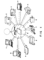
- FIG. 1 is a view of an overall configuration of an information transmission system according to an embodiment of the present invention.
- FIG. 1 shows a personal computer with pen input 2, an electronic notebook 3, a word processor 4, a printer 5, a copier 6, a telephone 7, a facsimile 8, an electronic camera (also called a steal camera) 9, a workstation 110, and a personal computer 11.
- a personal computer with pen input 2
- an electronic notebook 3 a word processor 4
- a printer 5 a copier 6, a telephone 7, a facsimile 8, an electronic camera (also called a steal camera) 9
- workstation 110 a personal computer 11.
- other types of information apparatuses may be used instead.
- the data-format of one of information apparatuses is different from that of other of information apparatuses.
- An IC card 1 as a card-like portable memory medium contains a nonvolatile semiconductor memory element. Specifically, this semiconductor memory element is an electrically erasable PROM (EEPROM, also known as a flash memory) that enables the stored data to be erased and rewritten electrically.
- EEPROM electrically erasable PROM
- This IC card 1 intervenes between various types of information apparatuses 2 through 11 as transmission means, which exchange data with each other.
- the various types of information apparatuses 2 through 11 are connected to a transmission line 12 (a public line of telecommunication or a LAN (local area network)), through which data exchange can be effected.
- a transmission line 12 a public line of telecommunication or a LAN (local area network)
- All the information apparatuses 2 through 11 are each provided with connectors that permit installation and removal of an IC card 1 and with transmission means for directly or indirectly accessing the internal memory of the IC card 1.
- This transmission means creates data and data-format information and identification information, and then send them to the IC card 1 and the transmission line 12.
- Any one of the information apparatuses is previously provided with information about a method of reading the data unique to each of the other information apparatuses.
- the information about a reading method includes: the word identification code; the number of bits per word; encoding information (the sampling frequency, the quantization coefficient, symbol codes): a decoding program itself; and image attribute information (the frame size, scanning procedure).
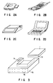
- the specification of the IC card 1 may or may not comply with the standards prescribed by JEIDA (the Japan Electronic Industry Development Association). Because the IC card does not require an internal power supply, it is desirable in terms of portability that the IC card 1 should be designed to a size smaller than the standards prescribed by JEIDA, for example, half the prescribed size.
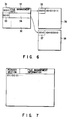
- Some information apparatuses are already provided with a slot and a connector in which an IC card conforming to the JEIDA standards can be installed. In order that the slot and connector can be used for a half-size IC card 1 without modification, an adapter 70 that allows installation and removal of the IC card of FIG. 3 has been proposed.
- the adapter 70 whose size and connector pin arrangement comply with the JEIDA standards, is designed to be inserted in a slot conforming to the JEIDA standards already provided in an existing information apparatus.
- the adapter 70 contains a logic circuit for performing signal conversion for the exchange of signals between IC cards.
- a driving power supply may be incorporated in the adapter 70 or the adapter 70 may be powered externally.
- the adapter 70 is provided with an injector 71 that facilitates installation and removal of the IC card 1. Of course, providing an information apparatus with an connector may be replaced with connecting an IC read/write unit to an information apparatus.
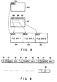
- FIG. 4 shows data transmitted through an IC card 1 or a transmission line 12.
- Data 64 generated at transmission means 60 on the information generation side (the transmission side), any one of the various types of information apparatuses 2 through 11, is written together with information source description data 63 in the IC card 1, or is sent to reception means 61 on the reception side via the transmission line 12.
- the information source description data 63 includes data-format information unique to an information apparatus on the transmission side and the identification information unique to an information apparatus on the transmission side.
- the reception means 61, an information apparatus on the reception side even if it is not previously given information on a method of reading data from an information apparatus on the transmission side, can read the data transmitted from the transmission means 60, an information apparatus on the calling party, according to the reading method contained in the information source description data 63.
- the reception means 61 if it is previously given information on a method of reading the data unique to an information apparatus on the calling party and holds it, can read the data according to the method of reading the data unique to an information apparatus on the calling party selected on the basis of the identification information.
- the interfacing of the internal circuit of the IC card 1 with an external information apparatus and an external power supply unit is effected by an address signal terminal 20, a data signal terminal 21, a control signal terminal 22, a status signal terminal 23, and an external power supply terminal 24.
- the power supplied from the external power supply terminal 24 is converted by a regulator 26 into the necessary power supply voltage, which is supplied to the internal circuit.
- the voltage supplied to the external power supply terminal 24 is generally 5 V.
- a different voltage for example, a high voltage of nearly 18 V may be supplied.
- the IC card 1 can operate in two operating modes: the memory mode and the I/P mode.
- the memory mode is a mode in which an external information apparatus directly specifies the address of the non-volatile semiconductor memory element 27 in the IC card 1. In this mode, the IC card 1 acts as an expansion memory like the internal memory in an external information apparatus.
- the I/O mode the IC card 1 is treated as a file unit. In this mode, an external information apparatus does not directly specifies the address of the nonvolatile semiconductor memory element 27 in the IC card.
- a file in the IC card is accessed by an external information apparatus by sending a data signal and a control signal to the controller 25. Because the file information is also stored in the nonvolatile semiconductor memory element 27, the controller 25 generates a file information address, accessing the nonvolatile semiconductor memory element 27 via a signal line 28 by using the file information address as an ADR signal, treating the file information read from the nonvolatile semiconductor memory element 27 via the I/O line 29 as a data signal, outputting this data signal and a status signal to an external information apparatus via the data signal terminal 21 and the status signal terminal 23, respectively. What is important here is that the address of each file information item in the nonvolatile semiconductor memory.element 27 has been determined previously in order to access at least the file information. The information for accessing may contain only a pointer or the file information itself. The address information is stored in a particular location in the memory space of the nonvolatile semiconductor memory element 27, for example, the first location or the last location.
- the controller 25 obtains information including the start address of the file, the memory size, and the type of data in the nonvolatile semiconductor memory element 27 on the basis of the file information read from the memory element 27, and outputs this file information to an external unit via the data signal terminal 21. At the same time, it outputs a status signal indicating file information to the external unit via the status signal terminal 23.
- the controller 25 on the basis of these signal, generates an actual address of the nonvolatile semiconductor memory element 27 as an ADR signal.
- the controller 25 accesses the nonvolatile semiconductor memory element 27, converts the data taken in from the I/O line 29 into a necessary form, and outputs this converted signal to an external unit via the data signal terminal 21. At the same time, it outputs an status signal indicating file data to the external unit via the status signal terminal 23.
- the controller 25 To write a file, the controller 25 first recognizes a blank area of the nonvolatile semiconductor memory element 27 from the file information, determines the start address at which a file is to be stored, sends the file data sent from an external unit via the data signal terminal 21 together with a PGM signal (a program signal) indicating the write mode to the nonvolatile semiconductor memory element 27 via the I/O line 29, and writes the file data in the memory area.
- Supplying the PGM signal may be replaced with causing the regulator 26 to supply a high voltage for a program differing from the voltage normally supplied to the nonvolatile semiconductor memory element 27, depending on the situation.
- the controller 25 writes the file data in the non-volatile semiconductor memory element 27, while counting the amount of data written into, and at the time when the writing is completed, adds the start address of the file data and its data size to the file information. In addition to this, data on the-type of data is also added to the file information.
- Another method of accessing the file information by a combination of an address signal and a control signal can be considered.
- the address space of the nonvolatile semiconductor memory element 27 is logically divided into a file data area and an area for attribute information including file information. Then, using an address signal and a control signal indicating the area of attribute information, the nonvolatile semiconductor memory element 27 is accessed. The operation for this is the same as that in the I/O mode and its explanation will be omitted.
- the logical dividing of the address space into the file data area and the attribute information area facilitates access. To deal with the file data, however, it is necessary to perform address control with an external unit. In storing the information unique to the IC card 1 including the memory size, the type of element, and the operating speed, the logical division is effective.
- FIG. 6 shows an example of storing a pointer and the file management information in a memory area different from that for the file data.
- pointers 31 and 33 representing the start addresses are written in the first level of hierarchy.
- the first level of hierarchy contains the attribute information on the file data stored in the memory area indicated by each pointer, the identification information for identifying an information apparatus on the data transmission side, and the file management information items 32 and 34.
- the first level also contains information about a method of reading data with an information apparatus on the data transmission side, as information source description data 30.
- the memory areas in the second level of hierarchy indicated by each pointer each store file data items. Such a hierarchic structure is effective in terms of memory efficiency. As shown in FIG.
- FIG. 7 shows an example of storing part of the file information of FIG. 6 as subfile information in a memory area different from that in which file information is stored.
- speech and moving-picture data are handled in seconds or in frames. Encoding compression and decoding are also generally effected in these units. This enables the head of the speech data to be located and the moving-picture data to be reproduced from a given frame.
- the speech data and the moving-picture data are stored as file data items 39a, 39b, and 39c in separate memory areas in seconds or in frames.
- subfile information 39f is placed as the underlying level of hierarchy.
- pointers 39g, 39h, and 39i of the individual data items 39a, 39b, and 39c are written.
- FIG. 9 shows an example of storing the above file management information.
- the number of words or the data length of the file management information may varies with the information apparatus serving as an information source. Therefore, to increase the memory efficiency, it is desirable that those information items should be divided word by word and written continuously.
- pairs of pointers 41, 44, and 47 and word data items 42, 45, and 48 are written in sequence, dividing the pairs by identifiers 40, 43, and 46, ... (IDs) representing the type of data, and identifier 49 indicating an end is written at the end.
- IDs representing the type of data
- the IC card 1 may be constructed as shown in FIG. 10.
- FIG. 10 the same parts as those in FIG. 5 are indicated by the same reference numerals.
- the nonvolatile semiconductor memory element 27 is of the type where the number of writes is limited, the service life of the nonvolatile semiconductor memory element 27 can be made longer.
- the program can be accessed directly by an external apparatus, such as a personal computer.
- the addition of the semiconductor memory element 30 has a wider variety of application.
- an image generated by the electronic camera 3 or the copier 6 is processed at the workstation 4. After that, the processed image is transmitted to a third party via the facsimile 8 or the telephone 7 or outputted on the printer 5. It should be noted here that even if each information apparatus is not previously provided with information about a method of reading the data unique to the other information apparatus, it is possible to read the sent data according to the information source description data (information on a reading method) sent together with the data.
- FIG. 11 shows a more concrete use of the IC card.
- the role of each information apparatus is expressed as an input function I, an output function O, a storage function S, a processing function P, and a distribution (transmission) function D.
- the electronic camera 9 serves as the input function I.
- the image data taken by the electronic camera 9, together with the information source description data, is stored in the IC card 1 or is transmitted to another information apparatus via the transmission line 12.
- the IC card 1 is conveyed to a desired copier 6 with human intervention, and is installed in a connector of the copier 6. At this time, the IC card 1, like the transmission line 12, serves as the distribution function D.
- the copier 6 reads the image data according to the sent information source description data.
- the image data read in the copier 6 is printed on paper.
- the copier 6 fills the role of the output function O.
- the IC card 1 is carried to a desired personal computer 11 with human intervention and is installed in a connector of the personal computer 11.
- the personal computer 11 performs a suitable image and an editing process, such as adding a character title, on the image data read according to the information source description data, and stores the processed image data in the built-in hard disk.
- the personal computer 11 fills the roles of the processing function P and the storage function S.
- the image data subjected to the image and editing processes at the personal computer 11 is stored in the IC card 1.
- the IC card 1 is then carried to a desired copier 6 with human intervention and is installed in a connector of the copier 6. At this time, the IC card 1 serves as the distribution function D.
- the image data read in the copier 6 is printed on paper.
- FIG. 12 shows a concrete internal.structure of the IC card of FIG. 10.
- the IC card 1 is provided with a pin connector 90.
- the pin connector 90 complies with JEIDA/PCMCIA and is designed for a 68-pin arrangement.
- a plurality of nonvolatile semiconductor memory elements 93 and 94 acting as the main memory and a read-only attribute memory 92 for storing the attribute information unique to the IC card are connected via a memory control section 91.
- the number of nonvolatile semiconductor memory elements 93 and 94 is not limited to more than one but may be one.
- each type of signal input and output has its own pin.
- D7-0 Two-way 8-bit data bus.
- the card is at high impedance in any mode other than the data read mode.
- A9-1 Address signal -CE1: Card enable signal. In accessing the IC card, -CE1 signal is kept low.
- -OE Output enable signal.
- -OE signal is kept low when the card attribute information is read from the attribute memory or information is read from the configuration register. When mapping is effected for a memory card, information can be read from a register set in the IC card.
- -WE Write enable signal. With this card, when information is written into the attribute memory or the configuration memory, -WE is kept low.
- RDY/-BSY This signal functions as an interrupt request signal (-IREQ) when configuration is made for an I/O card.
- -IREQ interrupt request signal
- the controller state machine
- this signal goes low.
- an interrupt occurs when the erase operation or the program has been completed.
- the level mode or the pulse mode can be selected by setting the configuration option register. Since this signal is outputted at an open drain, pull-up is necessary on the part of the host.
- -IORD This signal is used to read information from a register set in the IC card when configuration is made for an I/O card.
- -IOWR This signal is used to write information in a register set in the IC card when configuration is made for an I/O card.
- RESET This signal is used to reset the internal circuitry of the IC card.
- -CD1 IC card sense signal. The IC card outputs a low-level signal. When the host interface has sensed the low IC-card sense signal and the low-level signal from the IC card, this means that the IC card is inserted properly. This signal is also used to sense whether the IC card is removed or not.
- -INPACK Input response signal.
- This signal goes low when -CE and -IORD are low and the address on the address bus has coincided with the I/O port in the IC card.
- This signal is at an open drain and is at high impedance with the IC memory IC card interface. It is recommended that the host should not use -INPACK signal for buffer control. This signal is not supported when reading is effected at the memory card interface or when information is read from the attribute memory.
- VCC A 5-V operating power supply.
- VPP1 A 12-V program power supply. This is used when information is written in the attribute memory. The voltage of a VPP1 for an information apparatus which does not write information in the attribute memory, must be 5 V (VCC). Normally, a dedicated programmer is used for writing information in the attribute memory.
- GND Ground
- the attribute information about the IC card 1 includes: a physical layer including the shape of the card, the dimensions and the electrical characteristics, a basic interchangeable layer for determining the basic structure of a data structure, and information necessary for physically accessing a card, such as the device, the capacity, and the access speed of a memory card. Since the attribute information does not necessarily have to be rewritable, there is no problem if it is stored in the read-only attribute memory 92. In addition to this, a data format layer, a data structure layer, and information higher in level that a system inherent layer are also included in the attribute information, but these pieces of information are not necessarily stored in the attribute memory 92, but may be written in the non-volatile memories 93 and 94.
- the attribute memory 92 is basically a nonvolatile memory.
- the layer information may be selectively stored in either the nonvolatile memories 93 and 94 or the attribute memory 92 as required. Since the amount of the attribute information is much smaller that of the data, a low-cost memory with a smaller storage capacity can be used for the attribute memory 92.
- memories with a limited number of writes like EEPROMs (electrically erasable programmable ROMs), are used for the nonvolatile memories 93 and 94, the service life of these memories 93 and 94 can be made longer.
- FIG. 13 shows various registers provided in the memory control section 91.
- FIG. 14 illustrates the connections for a read and a write operation.
- the non-volatile memories 93 and 94 are controlled by an address register 95 and a data register 96 in the memory control section 91.
- the address register 95 accesses the non-volatile memories 93 and 94 via signal line MA31-0 according to signal D7-0 supplied from an external unit.
- the memory areas of the nonvolatile memories 93 and 94 are divided into blocks, each consisting of, for example, PAGE 0 to PAGE 15.
- the data register 96 accesses the data buffers of the nonvolatile memories 93 and 94 via signal line MD7-0 according to the signal supplied over D7-0.
- FIG. 15 shows the data stored in the attribute memory 92.
- the card attribute information 97 and the card control information 98 are written.
- the memory control section 91 accesses the card attribute information in the attribute memory 92 via signal line A9-1.
- the card attribute information read from the attribute memory 92 is returned to the memory control section 91 via signal line D7-0. It is desirable that all the data to be stored in the attribute memory 92 should be written in even addresses. Writing data in this way is convenient for common use of these memories because data is written in even addresses in a 16-bit memory and an 8-bit memory.
- FIGS. 16, 17, and 18 show the program operating procedure, the memory reading procedure, and the chip/block erasing procedure of the IC card of FIG. 11, respectively. Before explaining each procedure, each command handled by the IC card will be enumerated below.
- Data is read from the memory address previously set in response to the request from an external information apparatus. Data reading is effected by reading the data registers in the IC card consecutively. The address is automatically incremented and can continue the reading beyond a page boundary. At a block boundary, the address is not incremented automatically. It takes 15 microseconds to access a page, and in the meantime, the card is in a busy state. The external unit and the controller must judge the ready/busy state on a page boundary. It must not be expected tacitly that the memories are set in the read mode.
- the memory block at a given memory address is electrically erased in unison.
- an interrupt occurs after the erasing operation has been completed.
- the completion of the erasing operation is sensed by RDY-BSY (ready/busy) signal or the status signal.
- the memory chip containing the address previously set is erased. In executing this command, the host must recognize a chip boundary. When the card is operating in the I/O mode, an interrupt occurs after the erasing operation has been completed. When the card is operating in the memory mode, the completion of the erasing operation is sensed by RDY-BSY (ready/busy) signal or the status signal.
- RDY-BSY ready/busy
- Data is written in the memory page by page, and verification is automatically performed. Before execution of the program command, the address must be set and a page of data to be written must be transmitted according to the data buffer write command. For a program in the same block, its address need not be set again at a page boundary. The address is automatically incremented at a page boundary.
- the address is not incremented automatically at a block boundary. This is because the status must be fixed in a manner that points at the memory chip address for reading the status according to the status read command following the program.
- the program operation on the continuous page areas is effected in ascending order of page addresses, not in random order of page addresses. Data can be overwritten on the same page a maximum of 10 times, for example.
- -WP stands for WRITE PROTECT SWITCH STATUS for write disable and write enable.
- WSRDY stands for MEMORY STATUS READY for ready and busy states.
- SUSPEND MULTI-BLOCK ERASE SUSPENDED indicates that operation is suspended by a multi-block erase suspend command. Because the current IC card does not use a multi-block erase suspend command, the card is always in a suspended state.
- REU "0" represents Reserved for Future Use (Always "0"). It is always at 0 in a reserved bit.
- FAIL indicates the pass/fail state after an erase or program operation has been completed. When FAIL goes to 0, this means a pass, and when it goes to 1, this means a failure (error).
- a reset command when a status read command is executed after a memory read operation, a reset command must be executed before the execution of the status read command. This is because in the course of reading information from the memory, the status read command cannot be executed. Since the current card does not read the redundant portion, the memory read operation ends with a suspended state.
- the memory address from which the status is to be read normally, the memory address from which the status is to be read must be set in advance, the address need not be set immediately after a block erase, a multi-block erase, or a chip erase command has been executed. A status read command can be accepted even in a busy state.
- This command is used to read a 2-byte JEDEC ID. All bytes in the address register are set at 00h before the execution of an ID read command.
- This command is used to write data to be programmed in the data buffer.
- the address to be programmed must be set before the execution of the data buffer write command. Since in the same block, the address is automatically incremented, an address need not be set at a page boundary.
- the operation can be suspended by a reset command. While the reset command is being executed, the card is in a busy state for a certain period of time.
- This command is used to read data from the data buffer.
- the verify result can be judged bit by bit. "0" means that data has been written properly, and "1" means that an error has occurred in the writing.
- the card and all the memories are reset. After the execution of the reset command, the card is brought in a busy state for nearly three microseconds. The reset command can be accepted even in the busy state.
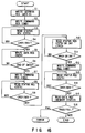
- step S1 The program operation in FIG. 16 begins by writing an address in the address register at step (S1). Then, a command is written in the data buffer (S2) and the status is read from the status register (S3). At this time, the controller sends an address and a command to the memory. Then, at step S4, the controller checks to see if the memory is either ready or busy. If it is busy, control returns to step S3. If it is ready, step S5 is executed. At step S5, data is transferred to the memory via the data register. Next, at step S6, it is judged whether or not the data has ended. If it has not ended, control returns to step S5. If it has ended, at step S7, a command is written in the command register.
- step S8 the status is read from the status register. At this time, the controller transfers a command to the memory.
- step S9 the controller checks to see if the memory is either ready or busy. If it is busy, control returns to step S8. If it is ready, at step S10, data is read from the status register. Then, at step S11, the status of the memory is checked. Next, at step S12, a command is written in the command register. Then, at step S13, data is read from the status register. At this time, the controller transfers a command to the memory.
- step S14 the controller checks the status of the memory. If the memory is busy, control returns to step S12. If it is ready, at step S15, data is read from the data register. Finally, at step S16, a check is made for PASS or FALL. If is PASS, it means an end. If it is FALL, an error is out putted.
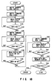
- a memory read operation of FIG. 17 begins by writing an address in the address register at step S21. Then, at step S22, a read command is written in the command register. At step 23, data is read from the status register. At this time, the controller transfers an address and a command to the memory. Then, at step S24, the controller checks to see if the memory is either busy or ready. If it is busy, control returns to step S23. If it is ready, step S25 is executed. At step 25, data continues to be read from the data register until at step 26, a read end is sensed. During the time when data is being read, at step S27, a page boundary is checked. If no page boundary is sensed, control goes back to step S25. If a page boundary is sensed, control returns to step S22.
- step S38 data is read from the status register or INT. Then, at step S39, the status of the memory or INT is checked. Then, at step S40, a status read command is written in the command register. At step S41, data is read from the status register. At this time, the controller transfers a command to the memory. At step S42, the controller checks the status of the memory. If the memory is busy, control returns to step S41. If it is ready, at step S43, data is read from the data register. Finally, at step S44, a check is made for PASS or FALL. If it is PASS, it means an end. If it is FALL, an error is outputted.
- an IC card When an IC card is used as a transmission medium, even an information apparatus without a function compatible with a transmission line can be built in an information transmission network. Additionally, the use of IC cards eliminates the trouble of building a transmission line, thereby making it possible to build an information transmission network with relative ease. Because a nonvolatile semiconductor memory element is used as the internal memory of the IC card, a power supply need not be built in the card. Thus, the IC card can be made so much smaller and its portability can be improved. The danger of losing the data becomes lower, improving the data retaining reliability. Furthermore, the trouble of replacing dead batteries can be eliminated.
Applications Claiming Priority (6)
| Application Number | Priority Date | Filing Date | Title |
|---|---|---|---|
| JP33771292 | 1992-12-18 | ||
| JP33771292 | 1992-12-18 | ||
| JP337712/92 | 1992-12-18 | ||
| JP23892/93 | 1993-02-12 | ||
| JP2389293 | 1993-02-12 | ||
| JP5023892A JPH06236316A (ja) | 1992-12-18 | 1993-02-12 | 情報伝送システム |
Publications (3)
| Publication Number | Publication Date |
|---|---|
| EP0602997A2 true EP0602997A2 (de) | 1994-06-22 |
| EP0602997A3 EP0602997A3 (de) | 1994-10-05 |
| EP0602997B1 EP0602997B1 (de) | 2001-07-11 |
Family
ID=26361333
Family Applications (1)
| Application Number | Title | Priority Date | Filing Date |
|---|---|---|---|
| EP93310231A Expired - Lifetime EP0602997B1 (de) | 1992-12-18 | 1993-12-17 | Informationsübertragungssystem |
Country Status (4)
| Country | Link |
|---|---|
| US (1) | US5930818A (de) |
| EP (1) | EP0602997B1 (de) |
| JP (1) | JPH06236316A (de) |
| DE (1) | DE69330422T2 (de) |
Cited By (6)
| Publication number | Priority date | Publication date | Assignee | Title |
|---|---|---|---|---|
| FR2711832A1 (fr) * | 1993-10-27 | 1995-05-05 | Intel Corp | Carte de mémoire non volatile avec indication prêt occupé et minimisation de compte de broches. |
| ES2112199A1 (es) * | 1994-12-29 | 1998-03-16 | Motorola Inc | Metodo y aparato para la seleccion y gestion con retardo de preferencias personales en aparatos programables. |
| ES2112197A1 (es) * | 1994-12-29 | 1998-03-16 | Motorola Inc | Metodo y aparato para la seleccion y gestion con prediccion de preferencias personales en aparatos programables. |
| ES2112198A1 (es) * | 1994-12-26 | 1998-03-16 | Motorola Inc | Metodo y aparato para la seleccion y gestion de preferencias personales en aparatos programables mediante memoria de preferencias. |
| EP0902589A2 (de) * | 1997-09-03 | 1999-03-17 | Matsushita Electric Industrial Co., Ltd | Digitales Abbildungssystem |
| EP0786715A3 (de) * | 1996-01-29 | 1999-06-09 | Canon Kabushiki Kaisha | Elektronisches Gerät |
Families Citing this family (18)
| Publication number | Priority date | Publication date | Assignee | Title |
|---|---|---|---|---|
| JPH06312593A (ja) | 1993-04-28 | 1994-11-08 | Toshiba Corp | 外部記憶装置、外部記憶装置ユニットおよび外部記憶装置の製造方法 |
| JPH0737049A (ja) * | 1993-07-23 | 1995-02-07 | Toshiba Corp | 外部記憶装置 |
| JP3383398B2 (ja) * | 1994-03-22 | 2003-03-04 | 株式会社東芝 | 半導体パッケージ |
| JP3893480B2 (ja) | 1994-09-28 | 2007-03-14 | 株式会社リコー | デジタル電子カメラ |
| JPH0964240A (ja) | 1995-08-25 | 1997-03-07 | Toshiba Corp | 半導体装置および半導体装置の製造方法 |
| US6022763A (en) * | 1996-05-10 | 2000-02-08 | Kabushiki Kaisha Toshiba | Substrate for semiconductor device, semiconductor device using the same, and method for manufacture thereof |
| JPH09327990A (ja) * | 1996-06-11 | 1997-12-22 | Toshiba Corp | カード型記憶装置 |
| JPH10302030A (ja) * | 1997-02-28 | 1998-11-13 | Toshiba Corp | 接続装置、および情報処理装置 |
| US7034871B2 (en) * | 1997-11-24 | 2006-04-25 | Eastman Kodak Company | Capturing digital images to be transferred to an e-mail address |
| JP3452555B2 (ja) | 2000-07-31 | 2003-09-29 | 松下電器産業株式会社 | 携帯電話機及びデータ記録システム |
| US6748402B1 (en) * | 2001-04-02 | 2004-06-08 | Bellsouth Intellectual Property Corporation | System and method for converting and loading interactive pager address books |
| US7260658B2 (en) * | 2002-05-31 | 2007-08-21 | Oracle International Corporation | Verifying input/output command data by separately sending data to be written and information about contents of the data |
| US20030233590A1 (en) * | 2002-06-17 | 2003-12-18 | Henry Liu | Conversion device bult in with signal and level conversion circuits |
| EP1571813A1 (de) | 2004-03-02 | 2005-09-07 | LG Electronics, Inc. | Methode und Kommunikationssystem zum Übermitteln eines Bildes vom Anrufer an den angerufenen Teilnehmer welches den Anrufer identifiziert |
| WO2005098675A1 (en) * | 2004-03-26 | 2005-10-20 | Alex Mashinski | Exchange of newly-added information over the internet |
| KR100704037B1 (ko) * | 2005-04-15 | 2007-04-04 | 삼성전자주식회사 | 이종의 비휘발성 메모리를 가지는 데이터 저장장치와 그의구동 방법 |
| US8001432B2 (en) * | 2008-11-20 | 2011-08-16 | Lsi Corporation | Uninitialized memory detection using error correction codes and built-in self test |
| KR20170086345A (ko) * | 2016-01-18 | 2017-07-26 | 에스케이하이닉스 주식회사 | 메모리 칩 및 메모리 컨트롤러를 포함하는 메모리 시스템 |
Citations (4)
| Publication number | Priority date | Publication date | Assignee | Title |
|---|---|---|---|---|
| JPH02205443A (ja) * | 1989-01-31 | 1990-08-15 | Toshiba Corp | 携帯型データ処理装置 |
| EP0408132A1 (de) * | 1989-07-14 | 1991-01-16 | Océ-Nederland B.V. | System zur Verarbeitung von in Dateien organisierten Daten mit Steuerungsmodul |
| JPH03214310A (ja) * | 1990-01-19 | 1991-09-19 | Hitachi Ltd | マルチメディアメモリ装置 |
| EP0449493A2 (de) * | 1990-03-26 | 1991-10-02 | International Business Machines Corporation | Verfahren und Gerät zur Übertragung von Daten zwischen heterogenen Datenbanksystemen |
Family Cites Families (9)
| Publication number | Priority date | Publication date | Assignee | Title |
|---|---|---|---|---|
| US4829169A (en) * | 1985-07-01 | 1989-05-09 | Toppan Moore Company, Inc. | IC card having state marker for record access |
| US4874935A (en) * | 1986-03-10 | 1989-10-17 | Data Card Coprporation | Smart card apparatus and method of programming same |
| GB2206431B (en) * | 1987-06-30 | 1991-05-29 | Motorola Inc | Data card circuits |
| US5032927A (en) * | 1988-03-01 | 1991-07-16 | Fuji Photo Film Co., Ltd. | Image signal recording apparatus capable of recording compressed image data together with audio data |
| JP2959773B2 (ja) * | 1989-04-20 | 1999-10-06 | オリンパス光学工業株式会社 | 電子スチルカメラ |
| US5107743A (en) * | 1989-12-04 | 1992-04-28 | Decker Tom W | Piano teaching device and method |
| CA2103395C (en) * | 1992-11-24 | 2004-08-17 | Masakazu Suzuoki | Apparatus and method for providing texture of a moving image to a surface of an object to be displayed |
| JP3103597B2 (ja) * | 1993-08-11 | 2000-10-30 | リーバイ ストラウス アンド カンパニー | コンピュータ制御された機械のための音声を用いたトラブルシューティングシステム |
| US5511000A (en) * | 1993-11-18 | 1996-04-23 | Kaloi; Dennis M. | Electronic solid-state record/playback device and system |
-
1993
- 1993-02-12 JP JP5023892A patent/JPH06236316A/ja active Pending
- 1993-12-17 DE DE69330422T patent/DE69330422T2/de not_active Expired - Lifetime
- 1993-12-17 EP EP93310231A patent/EP0602997B1/de not_active Expired - Lifetime
-
1997
- 1997-08-22 US US08/916,284 patent/US5930818A/en not_active Expired - Lifetime
Patent Citations (4)
| Publication number | Priority date | Publication date | Assignee | Title |
|---|---|---|---|---|
| JPH02205443A (ja) * | 1989-01-31 | 1990-08-15 | Toshiba Corp | 携帯型データ処理装置 |
| EP0408132A1 (de) * | 1989-07-14 | 1991-01-16 | Océ-Nederland B.V. | System zur Verarbeitung von in Dateien organisierten Daten mit Steuerungsmodul |
| JPH03214310A (ja) * | 1990-01-19 | 1991-09-19 | Hitachi Ltd | マルチメディアメモリ装置 |
| EP0449493A2 (de) * | 1990-03-26 | 1991-10-02 | International Business Machines Corporation | Verfahren und Gerät zur Übertragung von Daten zwischen heterogenen Datenbanksystemen |
Non-Patent Citations (2)
| Title |
|---|
| PATENT ABSTRACTS OF JAPAN vol. 14, no. 499 (M-1042) 31 October 1990 & JP-A-02 205 443 (TOSHIBA CORPORATION) 15 August 1990 * |
| PATENT ABSTRACTS OF JAPAN vol. 15, no. 495 (P-1288) 13 December 1991 & JP-A-03 214 310 (HITACHI LTD.) 19 September 1991 * |
Cited By (11)
| Publication number | Priority date | Publication date | Assignee | Title |
|---|---|---|---|---|
| FR2711832A1 (fr) * | 1993-10-27 | 1995-05-05 | Intel Corp | Carte de mémoire non volatile avec indication prêt occupé et minimisation de compte de broches. |
| ES2112198A1 (es) * | 1994-12-26 | 1998-03-16 | Motorola Inc | Metodo y aparato para la seleccion y gestion de preferencias personales en aparatos programables mediante memoria de preferencias. |
| ES2112199A1 (es) * | 1994-12-29 | 1998-03-16 | Motorola Inc | Metodo y aparato para la seleccion y gestion con retardo de preferencias personales en aparatos programables. |
| ES2112197A1 (es) * | 1994-12-29 | 1998-03-16 | Motorola Inc | Metodo y aparato para la seleccion y gestion con prediccion de preferencias personales en aparatos programables. |
| EP0786715A3 (de) * | 1996-01-29 | 1999-06-09 | Canon Kabushiki Kaisha | Elektronisches Gerät |
| US6686958B1 (en) | 1996-01-29 | 2004-02-03 | Canon Kabushiki Kaisha | Electronic apparatus for obtaining pickup data |
| US7630004B2 (en) | 1996-01-29 | 2009-12-08 | Canon Kabushiki Kaisha | Electronic apparatus |
| EP0902589A2 (de) * | 1997-09-03 | 1999-03-17 | Matsushita Electric Industrial Co., Ltd | Digitales Abbildungssystem |
| EP0902589A3 (de) * | 1997-09-03 | 1999-09-15 | Matsushita Electric Industrial Co., Ltd | Digitales Abbildungssystem |
| US6937356B1 (en) | 1997-09-03 | 2005-08-30 | Matsushita Electric Industrial Co., Ltd. | Digital imaging system |
| US7271930B2 (en) | 1997-09-03 | 2007-09-18 | Matsushita Electric Industrial Co., Ltd. | Printer unit |
Also Published As
| Publication number | Publication date |
|---|---|
| US5930818A (en) | 1999-07-27 |
| EP0602997A3 (de) | 1994-10-05 |
| JPH06236316A (ja) | 1994-08-23 |
| DE69330422T2 (de) | 2002-05-16 |
| DE69330422D1 (de) | 2001-08-16 |
| EP0602997B1 (de) | 2001-07-11 |
Similar Documents
| Publication | Publication Date | Title |
|---|---|---|
| EP0602997B1 (de) | Informationsübertragungssystem | |
| US5812814A (en) | Alternative flash EEPROM semiconductor memory system | |
| CN101313287B (zh) | 经由嵌入式控制器初始化快闪存储设备 | |
| JP2724046B2 (ja) | Icメモリカードシステム | |
| US6789158B2 (en) | Method of rewriting program in a flash microcomputer | |
| US7177975B2 (en) | Card system with erase tagging hierarchy and group based write protection | |
| US6851018B2 (en) | Exchanging operation parameters between a data storage device and a controller | |
| JP3718578B2 (ja) | メモリ管理方法及びメモリ管理装置 | |
| EP0528280A1 (de) | Aufzeichnungsgerät für eine Speicherkarte | |
| US6128675A (en) | Memory device having plurality of flash memories with a flash memory controlling circuit | |
| US5604917A (en) | IC memory card having masking function for preventing writing of data into a fixed memory area | |
| KR100986884B1 (ko) | 외부 접속 기기, 호스트 기기 및 데이터 통신 시스템 | |
| JPH08263361A (ja) | フラッシュメモリカード | |
| US20060224821A1 (en) | System for parallel updating flash memory and method for the same | |
| US20060026340A1 (en) | Memory card, card controller mounted on the memory card, and device for processing the memory card | |
| EP0890955B1 (de) | Speichervorrichtung sowie Datenlese- und Schreibverfahren | |
| KR100987205B1 (ko) | 외부 접속 기기, 호스트 기기 및 데이터 통신 시스템 | |
| US5829014A (en) | Method of supervising storage of data in a memory card having EEPROM and a memory card system using the same | |
| US6954815B2 (en) | Microcomputer with universal serial bus interface circuit and method of controlling the same | |
| TW200300257A (en) | Recording device | |
| JP3017524B2 (ja) | Icメモリカードにおけるデータ記録方法およびicメモリカードシステム | |
| JP2001005928A (ja) | Icカード | |
| JPH07141479A (ja) | Icメモリカードおよびそのicメモリカードを使用したファイル管理システム | |
| JP3190421B2 (ja) | Icメモリカードシステム | |
| JP2005100446A (ja) | 情報伝送システム及び情報伝送方法 |
Legal Events
| Date | Code | Title | Description |
|---|---|---|---|
| PUAI | Public reference made under article 153(3) epc to a published international application that has entered the european phase |
Free format text: ORIGINAL CODE: 0009012 |
|
| 17P | Request for examination filed |
Effective date: 19940104 |
|
| AK | Designated contracting states |
Kind code of ref document: A2 Designated state(s): DE FR GB |
|
| PUAL | Search report despatched |
Free format text: ORIGINAL CODE: 0009013 |
|
| AK | Designated contracting states |
Kind code of ref document: A3 Designated state(s): DE FR GB |
|
| 17Q | First examination report despatched |
Effective date: 19981113 |
|
| RIC1 | Information provided on ipc code assigned before grant |
Free format text: 7G 06F 17/30 A, 7G 06F 15/02 B |
|
| GRAG | Despatch of communication of intention to grant |
Free format text: ORIGINAL CODE: EPIDOS AGRA |
|
| GRAG | Despatch of communication of intention to grant |
Free format text: ORIGINAL CODE: EPIDOS AGRA |
|
| GRAH | Despatch of communication of intention to grant a patent |
Free format text: ORIGINAL CODE: EPIDOS IGRA |
|
| GRAH | Despatch of communication of intention to grant a patent |
Free format text: ORIGINAL CODE: EPIDOS IGRA |
|
| GRAA | (expected) grant |
Free format text: ORIGINAL CODE: 0009210 |
|
| AK | Designated contracting states |
Kind code of ref document: B1 Designated state(s): DE FR GB |
|
| REF | Corresponds to: |
Ref document number: 69330422 Country of ref document: DE Date of ref document: 20010816 |
|
| ET | Fr: translation filed | ||
| REG | Reference to a national code |
Ref country code: GB Ref legal event code: IF02 |
|
| PLBE | No opposition filed within time limit |
Free format text: ORIGINAL CODE: 0009261 |
|
| STAA | Information on the status of an ep patent application or granted ep patent |
Free format text: STATUS: NO OPPOSITION FILED WITHIN TIME LIMIT |
|
| 26N | No opposition filed | ||
| PGFP | Annual fee paid to national office [announced via postgrant information from national office to epo] |
Ref country code: FR Payment date: 20101224 Year of fee payment: 18 |
|
| PGFP | Annual fee paid to national office [announced via postgrant information from national office to epo] |
Ref country code: GB Payment date: 20101215 Year of fee payment: 18 |
|
| PGFP | Annual fee paid to national office [announced via postgrant information from national office to epo] |
Ref country code: DE Payment date: 20101215 Year of fee payment: 18 |
|
| GBPC | Gb: european patent ceased through non-payment of renewal fee |
Effective date: 20111217 |
|
| REG | Reference to a national code |
Ref country code: FR Ref legal event code: ST Effective date: 20120831 |
|
| REG | Reference to a national code |
Ref country code: DE Ref legal event code: R119 Ref document number: 69330422 Country of ref document: DE Effective date: 20120703 |
|
| PG25 | Lapsed in a contracting state [announced via postgrant information from national office to epo] |
Ref country code: DE Free format text: LAPSE BECAUSE OF NON-PAYMENT OF DUE FEES Effective date: 20120703 Ref country code: GB Free format text: LAPSE BECAUSE OF NON-PAYMENT OF DUE FEES Effective date: 20111217 |
|
| PG25 | Lapsed in a contracting state [announced via postgrant information from national office to epo] |
Ref country code: FR Free format text: LAPSE BECAUSE OF NON-PAYMENT OF DUE FEES Effective date: 20120102 |