EP0601410B1 - Schaltungsanordnung zur Steuerung der Vorspannung eines Leistungsverstärkers für Hochfrequenzsignale - Google Patents
Schaltungsanordnung zur Steuerung der Vorspannung eines Leistungsverstärkers für Hochfrequenzsignale Download PDFInfo
- Publication number
- EP0601410B1 EP0601410B1 EP93119055A EP93119055A EP0601410B1 EP 0601410 B1 EP0601410 B1 EP 0601410B1 EP 93119055 A EP93119055 A EP 93119055A EP 93119055 A EP93119055 A EP 93119055A EP 0601410 B1 EP0601410 B1 EP 0601410B1
- Authority
- EP
- European Patent Office
- Prior art keywords
- voltage
- supplied
- radio
- circuit
- amplifying element
- Prior art date
- Legal status (The legal status is an assumption and is not a legal conclusion. Google has not performed a legal analysis and makes no representation as to the accuracy of the status listed.)
- Expired - Lifetime
Links
Images


Classifications
-
- H—ELECTRICITY
- H03—ELECTRONIC CIRCUITRY
- H03F—AMPLIFIERS
- H03F1/00—Details of amplifiers with only discharge tubes, only semiconductor devices or only unspecified devices as amplifying elements
- H03F1/02—Modifications of amplifiers to raise the efficiency, e.g. gliding Class A stages, use of an auxiliary oscillation
- H03F1/0205—Modifications of amplifiers to raise the efficiency, e.g. gliding Class A stages, use of an auxiliary oscillation in transistor amplifiers
- H03F1/0211—Modifications of amplifiers to raise the efficiency, e.g. gliding Class A stages, use of an auxiliary oscillation in transistor amplifiers with control of the supply voltage or current
- H03F1/0244—Stepped control
-
- H—ELECTRICITY
- H03—ELECTRONIC CIRCUITRY
- H03F—AMPLIFIERS
- H03F1/00—Details of amplifiers with only discharge tubes, only semiconductor devices or only unspecified devices as amplifying elements
- H03F1/30—Modifications of amplifiers to reduce influence of variations of temperature or supply voltage or other physical parameters
- H03F1/301—Modifications of amplifiers to reduce influence of variations of temperature or supply voltage or other physical parameters in MOSFET amplifiers
-
- H—ELECTRICITY
- H03—ELECTRONIC CIRCUITRY
- H03F—AMPLIFIERS
- H03F2200/00—Indexing scheme relating to amplifiers
- H03F2200/481—A resistor being used as sensor
-
- H—ELECTRICITY
- H03—ELECTRONIC CIRCUITRY
- H03F—AMPLIFIERS
- H03F2200/00—Indexing scheme relating to amplifiers
- H03F2200/483—A shunting switch being paralleled to the sensor
Definitions
- the present invention relates to a bias control circuit for a radio-frequency power amplifier adapted for use in a digital portable telephone system.
- a TDMA method is generally employed to perform alternate transmission and reception by using the same frequency.
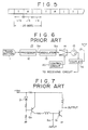
- a transmission time slot T, a reception time slot R and an idle time slot I are repeated temporally sequentially in one channel of a fixed frequency.
- each of the transmission time slot T, reception time slot R and idle time slot I has an equal duration of 20/3 msec.
- Transmission from a mobile station to a base station is performed during the transmission time slot T, and reception from the base station is performed during the reception time slot R.
- the idle time slot I is used for measuring the electric field intensity.
- Fig. 6 shows an exemplary transmitting circuit in a conventional mobile station.
- a sound signal is supplied from a transmitter 11 to a digital processor 12 to be thereby converted into a digital signal which is intermittent every transmission time slot T in conformity to a predetermined format, and the digital signal thus obtained is supplied to a modulator 13 to be converted into a transmission signal S13 through orthogonal modulation.
- the transmission signal S13 is supplied to a transmitting/receiving antenna 17 via a signal line consisting of a radio-frequency power amplifier 14, an isolator 15 and a common antenna coupler 16, so that the signal S13 is transmitted to the base station.
- the frequency band used for such transmission ranges, e.g., from 940 to 960 MHz.
- the transmission signal S13 is processed through orthogonal modulation and has an amplitude component, it is necessary for the amplifier 14 to execute power amplification of the signal S13 linearly. For this reason, the amplifier 14 needs to perform its operation in the class A or AB.
- a power transistor constituting the final stage of the power amplifier 14 deals with a considerably great power, so that the temperature in the transistor is much fluctuated due to the heat generated therefrom.
- the operating point of the transistor varies depending on the temperature.
- a bias control circuit 20 is incorporated in the transmitting circuit of Fig. 6 so that the idle current of the power transistor in the amplifier 14 is controlled to a predetermined value, thereby enabling the amplifier 14 to operate in the class A or AB regardless of the temperature fluctuation.
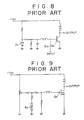
- Circuits shown in Figs. 7 to 9 may be contrived to serve as the power amplifier 14 and the control circuit 20 which satisfy the conditions mentioned.
- FIG. 7 to 9 For the purpose of simplifying the explanation, there drawings merely represent the theoretical connection or constitution.
- a power transistor Q1 in the final stage a transistor Q2 for applying a base bias to the transistor Q1, and a temperature compensating diode D1.
- a voltage including the terminal voltage of the diode D1 is supplied to the transistor Q2 as a base-emitter voltage thereof, so that the collector current of the transistor Q2 is stably maintained at a predetermined value regardless of any temperature fluctuation. Since such collector current is the base current of the transistor Q1, the idle current (collector current) of the transistor Q1 is also stabilized despite the temperature fluctuation.
- a power amplifying transistor Q3 is provided in the final stage. And the voltage obtained from a diode D3 is supplied as a base bias voltage to the transistor Q3. Therefore the idle current of the transistor Q3 is stably maintained at a predetermined value despite any temperature fluctuation.
- a power amplifying MOS FET Q4 in the final stage there are included a power amplifying MOS FET Q4 in the final stage, and a thermistor R4.
- the terminal voltage of the thermistor R4 is supplied to the MOS FET Q4 as a gate bias voltage thereof. Consequently the idle current of the FET Q4 is stably maintained at a predetermined value regardless of any temperature fluctuation.
- the circuit of Fig. 7 is effective when the transistor Q1 operates in the class A, but it is impossible to operate the transistor Q1 in the class AB since the collector current thereof is changed in accordance with the level of the transmission signal S13.
- the temperature compensating diode D1 needs to be thermally coupled to the transistor Q2.
- the temperature compensating diode D3 or the thermistor R4 needs to be thermally coupled to the transistor Q3 or the FET Q4.
- the transistor Q2 to be thermally coupled in the circuit of Fig. 7 is used merely for control, whereas the transistor Q3 or the FET Q4 to be thermally coupled in the circuit of Fig. 8 or 9 is used for power amplification of the transmission signal S13. Therefore, in the circuits of Figs. 8 and 9, the mounting or arrangement of the circuits and the component elements thereof need to be contrived in particular for averting interference and leakage of the signal S13.
- Bias control circuits for RF-amplifiers are known from e.g. US-A-5 128 629, EP-A-0 482 502 or EP-A-0 156 694.
- a bias control circuit for a radio-frequency power amplifier which performs linear power amplification of a radio-frequency signal supplied thereto intermittently at a predetermined repetition cycle.
- the bias control circuit comprises a bias voltage setting circuit for supplying a bias voltage of a predetermined value to a power amplifying element during a time period in which substantially none of the radio-frequency signal is supposed to be supplied to the power amplifying element, and setting the idle current of the power amplifying element to a predetermined value; and a sample and hold circuit for sampling and holding the bias voltage during the time period in which substantially none of the radio-frequency signal is supposed to be supplied to the power amplifying element. And during the following time period in which the radio-frequency signal is supplied to the power amplifying element, the output voltage of the sample and hold circuit is supplied as a bias voltage to the power amplifying element.
- the bias voltage setting circuit comprises a temperature compensating diode, a transistor supplied with the bias voltage including the terminal voltage of the diode, and a circuit for feeding back the output current in the power amplifying element to the transistor. And the output voltage of the transistor is supplied to the sample and hold circuit.
- the sample and hold circuit comprises an A-D converter for executing analog-to-digital conversion of the input voltage, a memory for holding the output data of the A-D converter, and a D-A converter for executing digital-to-analog conversion of the data held in the memory.
- the voltage from a power source is supplied to the power amplifying element regardless of the feedback circuit.
- Fig. 1 is a circuit diagram representing an exemplary embodiment of the invention.
- the final stage of a power amplifier 14 consists of a grounded-source field effect transistor (FET) Q14.
- the gate of the FET Q14 is grounded via a resistor R14, and the drain thereof is connected to a coil L14.
- a transmission signal S13 obtained from a modulator 13 is supplied via a drive stage 141 of the power amplifier 14 to the gate of the FET Q14, and its drain output is supplied to an isolator 15.
- a battery 31 for supplying a voltage of, e.g., 4V is used as a power source for the entire circuits, and a system controller 32 consists of a microcomputer or the like.
- a bias control circuit 20 comprises a bias voltage setting circuit 22 and a sample and hold circuit 23, and has the following configuration.
- the battery 31 is connected via a switch circuit 21 and a resistor R22 to the coil L14.
- a temperature compensating diode D22 and resistors R23, R24 are connected in series between the output of the switch circuit 21 and the ground, and the junction of the resistors R23 and R24 is connected to the base of a transistor Q22, whose emitter is connected to the junction of the resistor R22 and the coil L14.
- the collector of the transistor Q22 is connected via a resistor R25 to a voltage terminal T22 which is reverse in polarity to the battery 31.
- the bias setting circuit 22 is so constituted as mentioned.
- the sample and hold circuit 23 is connected to the collector of the transistor Q22, and the output voltage V23 of the circuit 23 is supplied as a bias voltage to the gate of the FET Q14 via a buffer voltage follower 24 and a coil L15.
- a pulse P21 turned to a high level (“H") during a transmission time slot T is obtained from the system controller 32 and, as shown in Fig. 2B, a pulse P23 turned to a high level during a predetermined short time period ⁇ at the start point of the transmission time slot T is also obtained from the system controller 32.
- the pulse P21 is supplied as a control signal to the switch circuit 21, which is thereby turned on during the high-level period of the pulse P21.
- the pulse P23 of the input voltage is supplied as a control signal to the sample and hold circuit 23, which then samples the input voltage during the high-level period of the pulse P23 and holds the sampled voltage during the low-level ("L”) period of the pulse P23.
- the digital signal outputted from the processor 12 is delivered during the time period excluding at least the start time period ⁇ from the transmission time slot T.
- the switch circuit 21 upon arrival of the transmission time slot T, the switch circuit 21 is turned on by the pulse P21 so that the operating voltages are applied respectively to the transistor Q22 and the FET Q14. Then the transistor Q22 is base-biased by the voltage including the terminal voltage of the diode D22, so that a constant collector current flows in the collector of the transistor Q22 regardless of any temperature fluctuation, whereby the collector is maintained stably at the constant collector voltage V22 despite occurrence of any temperature fluctuation.
- the collector voltage V22 is supplied as a gate bias voltage to the FET Q14 via a line consisting of the sample and hold circuit 23, the voltage follower 24 and the coil L15, so that a drain current I14 comes to flow in the FET Q14 corresponding to the bias voltage .
- the drain current I14 in the FET Q14 increases for example, it causes an increase of the voltage drop across the resistor R22 to lower the base bias voltage of the transistor Q22 as a result, whereby the collector current thereof is decreased to consequently lower the collector voltage V22. Since this signifies a drop of the gate bias voltage of the FET Q14, the drain current I14 thereof is decreased. More specifically, feedback is effected to the FET Q14 via the resistor R22, so that the drain current I14 thereof is stabilized against any temperature fluctuation.
- the voltage V22 during such period ⁇ is supplied from the sample and hold circuit 23 via the voltage follower 24 and the coil L15 to the gate of the FET Q14 as its bias voltage, so that such bias voltage causes a flow of the drain current I14 in the FET Q14.
- the collector voltage V22 is sampled during the time period ⁇ and then is held until the next time periods. Therefore, as shown in Fig. 2D, a DC voltage V23 equivalent to the collector voltage V22 during the time period ⁇ is outputted from the sample and hold circuit 23, and such voltage V23 is supplied as a bias voltage to the gate of the FET Q14 via the voltage follower 24.
- the drain current I14 of the FET Q14 is stably maintained at the predetermined value during the time periods, and the gate bias voltage V23 for causing a flow of such drain current I14 during the period ⁇ , is supplied continuously to the FET Q14 even after the period ⁇ , whereby the drain current I14 is stabilized against any temperature fluctuation even after the lapse of such period ⁇ .
- the FET Q14 is enabled by the bias voltage V23 to operate in the class A, and therefore it is rendered possible to cause a flow of the drain current I14 corresponding to the bias voltage V23, i.e., an idle current as shown in Fig. 2E.
- the transmission signal S13 is supplied to the FET Q14, so that the drain current I14 of the FET Q14 exceeds the idle current as shown in Fig. 2E and becomes proportional to the level of the transmission signal S13. It signifies that the FET Q14 operates in the class AB to consequently enhance the power efficiency.
- the idle current of the power amplifying FET Q14 is set to the predetermined value by controlling the gate bias voltage V23 applied to the FET Q14 during the time period ⁇ in which substantially none of the transmission signal S13 is supposed to be supplied to the FET Q14, and the gate bias voltage V23 obtained during such time period is sampled and held. Then the sampled voltage thus held is supplied as the gate bias voltage V23 to the FET Q14 during the subsequent period in which the transmission signal S13 is supplied thereto, whereby the idle current of the FET Q14 can be maintained at the set value despite occurrence of any temperature fluctuation in a wide range.
- the idle current of the FET Q14 can thus be maintained at the set value regardless of any temperature fluctuation, it becomes possible to retain the efficiency of the power amplifier 14 constant.
- the idle current of the FET Q14 can be kept continuously at the set value.
- the transmitting circuit 10 may be installed in an automobile trunk room or the like where sharp temperature fluctuation is prone to occur. Besides the above, there exists no necessity of adjusting the guaranty amount of temperature compensation with regard to the FET Q14, hence ensuring remarkable enhancement of the productivity.
- Fig. 3 shows another embodiment of the present invention, where the equivalent or same component circuits and elements as those employed in the aforementioned embodiment of Fig. 1 are denoted by the same reference numerals, and a detailed description thereof is omitted.
- a switch circuit 41 is connected in parallel to a feedback resistor R22, and a pulse P23 is supplied as a control signal to the switch circuit 41 in such a manner as to turn on the circuit 41 during a low level ("L") of the pulse P23 or to turn off the circuit 41 during a high level ("H") thereof.
- the bias voltage V23 is supplied to the FET Q14 with the aforementioned operation performed during the time periods.
- the resistor R22 is short-circuited by the switch circuit 41 and the voltage from the battery 31 is supplied directly to the FET Q14 without being lowered through the resistor R22, hence enhancing the efficiency of the source voltage.
- Fig. 4 shows a further embodiment of the present invention, where the equivalent or same component circuits and elements as those employed in the aforementioned embodiment of Fig. 1 are denoted by the same reference numerals, and a detailed description thereof is omitted.
- the embodiment of Fig. 4 represents an exemplary case of digitizing the sample and hold circuit 23 relative to the collector voltage V22. More specifically, the collector voltage V22 of the transistor Q22 is supplied to an A/D converter 51 to be thereby converted into digital data D22, which is then supplied to a latch memory 52. And the data D22 during the time period ⁇ is latched in the memory 52 in response to the pulse P23 and is extracted therefrom repeatedly.
- the data D22 thus extracted repeatedly is supplied to a D/A converter 53, which then produces a temporally continuous voltage corresponding to the voltage V22 during the time period ⁇ , i.e., the sampled-and-held voltage V23. Subsequently this voltage V23 is supplied as a bias voltage to the gate of the FET Q14.
- the final stage of the power amplifier 14 consists of a single-connection FET Q14.
- push-pull connection may also be employed, and a bipolar transistor may be used as well.
- the idle current of the power amplifying FET is set to a predetermined value by controlling the gate bias voltage of the FET during the time petiod in which substantially none of the transmission signal is supposed to be supplied to the FET, and the gate bias voltage during such time period is sampled and held. Then the sampled voltage thus held is supplied as a gate bias voltage to the FET during the subsequent supply period of the transmission signal. Therefore the idle current of the FET can be retained at the set value despite occurrence of any temperature fluctuation in a wide range.
- the idle current of the power amplifying FET can be maintained stably at the set value regardless of any temperature fluctuation, the efficiency of the power amplifier is retainable constant. And due to the advantage that the temperature compensation is updated every transmission of the intermittent signal, the idle current of the FET is maintained at the set value against any sharp temperature fluctuation. Furthermore, the idle current of the FET is kept free from the harmful influence derived from temperature fluctuation, so that the transmitting circuit may be installed in an automobile trunk room or the like where great temperature fluctuation is prone to occur. Besides the above, there is no necessity of adjusting the guaranty amount of temperature compensation relative to the FET, hence ensuring remarkable enhancement of the productivity.
Landscapes
- Engineering & Computer Science (AREA)
- Power Engineering (AREA)
- Amplifiers (AREA)
- Transmitters (AREA)
Claims (4)
- Schaltung (20) zur Steuerung der Vorspannung eines HF-Leistungsverstärkers (Q14) zur linearen Leistungsverstärkung eines mit bestimmter Wiederholrate intermittierend auftretenden Hochfrequenzsignals (S13), mit:einer Schaltung (22) zum Einstellen der Vorspannung, die während eines Zeitabschnitts, innerhalb dessen im wesentlichen kein Hochfrequenzsignal am Leistungsverstärkungselement anliegt, eine Vorspannung mit einem bestimmten Wert an ein Leistungsverstärkungselement anlegt, und zum Einstellen des Ruhestroms des Leistungsverstärkungselements auf einen bestimmten Wert; undeiner Abtast-Halte-Schaltung (23) zum Abtasten der Vorspannung während des Zeitabschnitts, innerhalb dessen im wesentlichen kein Hochfrequenzsignal am Leistungsverstärkungselement anliegt, und zum Halten der abgetasteten Spannung als Ausgangsspannung der Abtast-Halte-Schaltung; und weiter miteinem Mittel (32), durch das die Ausgangsspannung der Abtast-Halte-Schaltung während des folgenden Zeitabschnitts, innerhalb dessen das Hochfrequenzsignal am Leistungsverstärkungselement anliegt, das Leistungsverstärkungselement als Vorspannung beaufschlagt.
- Schaltung nach Anspruch 1, dadurch gekennzeichnet, daß die Schaltung zum Einstellen der Vorspannung enthält:eine Diode zur Kompensation der Temperatur;einen mit der Vorspannung, die die Anschlußspannung der Diode enthält, versorgten Transistor; undeine Schaltung zur Rückkopplung des Ausgangsstroms des Leistunsverstärkungselements an den Transistor;wobei die Ausgangsspannung des Transistors die Abtast-Halte-Schaltung beaufschlagt.
- Schaltung nach Anspruch 1, dadurch gekennzeichnet, daß die Abtast-Halte-Schaltung enthält:einen A/D-Wandler zur Analog/Digital-Wandlung der Eingangsspannung;einen Speicher zum Halten der Ausgangsdaten des A/D-Wandlers; undeinen D/A-Wandler zur Digital/Analog-Wandlung der in dem Speicher gehaltenen Daten.
- Schaltung nach Anspruch 2, dadurch gekennzeichnet, daß die Spannung einer Leistungsquelle unabhängig von der Rückkopplungsschaltung während des Zeitabschnitts der Versorgung des Hochfrequenzsignals das Leistungsverstärkungselement beaufschlagt.
Applications Claiming Priority (2)
| Application Number | Priority Date | Filing Date | Title |
|---|---|---|---|
| JP352065/92 | 1992-12-09 | ||
| JP35206592A JP3365428B2 (ja) | 1992-12-09 | 1992-12-09 | 高周波パワーアンプのバイアス制御回路 |
Publications (2)
| Publication Number | Publication Date |
|---|---|
| EP0601410A1 EP0601410A1 (de) | 1994-06-15 |
| EP0601410B1 true EP0601410B1 (de) | 1997-11-05 |
Family
ID=18421545
Family Applications (1)
| Application Number | Title | Priority Date | Filing Date |
|---|---|---|---|
| EP93119055A Expired - Lifetime EP0601410B1 (de) | 1992-12-09 | 1993-11-25 | Schaltungsanordnung zur Steuerung der Vorspannung eines Leistungsverstärkers für Hochfrequenzsignale |
Country Status (4)
| Country | Link |
|---|---|
| US (1) | US5406225A (de) |
| EP (1) | EP0601410B1 (de) |
| JP (1) | JP3365428B2 (de) |
| DE (1) | DE69315042T2 (de) |
Cited By (1)
| Publication number | Priority date | Publication date | Assignee | Title |
|---|---|---|---|---|
| US7031677B2 (en) | 2001-06-29 | 2006-04-18 | Infineon Technologies Ag | Optimization of the operating point of power amplifiers in mobile stations |
Families Citing this family (32)
| Publication number | Priority date | Publication date | Assignee | Title |
|---|---|---|---|---|
| JP2552089B2 (ja) * | 1994-05-23 | 1996-11-06 | 埼玉日本電気株式会社 | Fet増幅器の消費電力低減方式 |
| US5483191A (en) * | 1994-09-23 | 1996-01-09 | At&T Corp. | Apparatus for biasing a FET with a single voltage supply |
| US5589796A (en) * | 1994-11-01 | 1996-12-31 | Motorola, Inc | Method and apparatus for increasing amplifier efficiency |
| US5493255A (en) * | 1995-03-21 | 1996-02-20 | Nokia Mobile Phones Ltd. | Bias control circuit for an RF power amplifier |
| JP3366191B2 (ja) * | 1996-07-19 | 2003-01-14 | 沖電気工業株式会社 | アイドル電流補正回路及び低電圧駆動電子機器 |
| US5920808A (en) * | 1996-12-12 | 1999-07-06 | Glenayre Electronics, Inc. | Method and apparatus for reducing key-up distortion by pre-heating transistors |
| US6072995A (en) * | 1997-02-26 | 2000-06-06 | Ericsson Inc. | Flexible current control in power amplifiers |
| DE19737062A1 (de) * | 1997-08-26 | 1999-03-04 | Bosch Gmbh Robert | Verfahren und Schaltungsanordnung zur Einstellung eines Arbeitspunktes einer Transistorstufe |
| US6223056B1 (en) * | 1997-12-31 | 2001-04-24 | Samsung Electronics Co., Ltd. | Systems and methods for dynamically controlling a variable power amplifier |
| GB2334167B (en) * | 1998-02-07 | 2002-09-11 | Motorola Ltd | Amplifying circuit and method for determining optimal bias voltages therein |
| US6137354A (en) * | 1998-05-18 | 2000-10-24 | Omnipoint Corporation | Bypassable amplifier |
| US6008698A (en) * | 1998-05-18 | 1999-12-28 | Omnipoint Corporation | Amplifier with dynamically adaptable supply current |
| US6081161A (en) * | 1998-05-18 | 2000-06-27 | Omnipoint Corporation | Amplifier with dynamatically adaptable supply voltage |
| US6043706A (en) * | 1999-02-05 | 2000-03-28 | Ericsson Inc. | Methods and apparatus for controlling power amplifier quiescent current in a wireless communication device |
| US6111466A (en) * | 1999-03-22 | 2000-08-29 | Motorola, Inc. | Amplifier with feedback to provide bias adjustment |
| US6304129B1 (en) * | 1999-10-08 | 2001-10-16 | Ericsson Inc. | Compensation circuit and method for a power transistor |
| US6429746B1 (en) * | 1999-12-07 | 2002-08-06 | Nokia Networks Oy | System and method for auto-bias of an amplifier |
| US6351189B1 (en) * | 2000-07-31 | 2002-02-26 | Nokia Networks Oy | System and method for auto-bias of an amplifier |
| US6701138B2 (en) * | 2001-06-11 | 2004-03-02 | Rf Micro Devices, Inc. | Power amplifier control |
| DE10131654A1 (de) * | 2001-06-29 | 2003-01-16 | Infineon Technologies Ag | Arbeitspunktoptimierung von Sendeleistungsverstärkern in Mobilstationen |
| US6515545B1 (en) * | 2001-08-17 | 2003-02-04 | Harris Corporation | RF power amplifier transistor quiescent current checking and adjusting |
| US20030153287A1 (en) * | 2002-02-14 | 2003-08-14 | Tapio Kuiri | Method and apparatus for sensing operating temperature in a power amplifier |
| US6891438B2 (en) * | 2002-12-12 | 2005-05-10 | Northrop Grumman Corporation | Adaptive active bias compensation technique for power amplifiers |
| GB2400249B (en) * | 2003-03-31 | 2005-08-10 | Motorola Inc | Power amplifier and a RF transmitter and terminal including the amplifier |
| JP4791271B2 (ja) * | 2006-06-28 | 2011-10-12 | 富士通株式会社 | 増幅器制御装置 |
| US7768353B2 (en) * | 2008-06-13 | 2010-08-03 | Samsung Electro-Mechanics Company, Ltd. | Systems and methods for switching mode power amplifier control |
| US9166533B2 (en) * | 2009-07-30 | 2015-10-20 | Qualcomm Incorporated | Bias current monitor and control mechanism for amplifiers |
| JP2011044876A (ja) * | 2009-08-20 | 2011-03-03 | Yagi Antenna Co Ltd | バースト的に電波を送信する送信装置の送信増幅器 |
| US8319560B2 (en) * | 2009-10-05 | 2012-11-27 | Hittite Microwave Corporation | Switched active bias control and power-on sequencing circuit for an amplifier |
| US9166542B2 (en) | 2011-12-22 | 2015-10-20 | Murata Manufacturing Co., Ltd. | High frequency module and portable terminal using same |
| US12132473B2 (en) | 2023-03-13 | 2024-10-29 | Nxp Usa, Inc. | Switch with cascode arrangement |
| US12126338B1 (en) * | 2023-04-04 | 2024-10-22 | Nxp Usa, Inc. | Switch with cascode arrangement |
Family Cites Families (10)
| Publication number | Priority date | Publication date | Assignee | Title |
|---|---|---|---|---|
| GB1229585A (de) * | 1967-05-19 | 1971-04-28 | ||
| FR2560468A1 (fr) * | 1984-02-28 | 1985-08-30 | Lgt Lab Gen Telecomm | Dispositif de polarisation d'etage d'amplification a transistors et son utilisation dans un tel etage |
| GB8826918D0 (en) * | 1988-11-17 | 1988-12-21 | Motorola Inc | Power amplifier for radio frequency signal |
| CA2017904C (en) * | 1989-05-31 | 1993-11-16 | Shinichi Miyazaki | High frequency amplifier circuit capable of optimizing a total power consumption |
| JPH0466826U (de) * | 1990-10-16 | 1992-06-12 | ||
| TW198152B (de) * | 1990-10-18 | 1993-01-11 | Hitachi Seisakusyo Kk | |
| KR960000775B1 (ko) * | 1990-10-19 | 1996-01-12 | 닛본덴기 가부시끼가이샤 | 고주파 전력 증폭기의 출력레벨 제어회로 |
| US5204977A (en) | 1991-04-01 | 1993-04-20 | Motorola, Inc. | Apparatus and method of automatic gain control in a receiver |
| US5128629A (en) * | 1991-04-22 | 1992-07-07 | Hughes Aircraft Company | Method for controlling the output power of digital cellular telephones |
| SE470035B (sv) * | 1992-03-17 | 1993-10-25 | Ericsson Ge Mobile Communicat | Anordning för eliminering av offsetfel i en effektreglerkrets för ett pulsat sändarslutsteg |
-
1992
- 1992-12-09 JP JP35206592A patent/JP3365428B2/ja not_active Expired - Fee Related
-
1993
- 1993-11-25 DE DE69315042T patent/DE69315042T2/de not_active Expired - Fee Related
- 1993-11-25 EP EP93119055A patent/EP0601410B1/de not_active Expired - Lifetime
- 1993-11-30 US US08/158,766 patent/US5406225A/en not_active Expired - Fee Related
Cited By (1)
| Publication number | Priority date | Publication date | Assignee | Title |
|---|---|---|---|---|
| US7031677B2 (en) | 2001-06-29 | 2006-04-18 | Infineon Technologies Ag | Optimization of the operating point of power amplifiers in mobile stations |
Also Published As
| Publication number | Publication date |
|---|---|
| JPH06177658A (ja) | 1994-06-24 |
| EP0601410A1 (de) | 1994-06-15 |
| DE69315042T2 (de) | 1998-06-04 |
| DE69315042D1 (de) | 1997-12-11 |
| JP3365428B2 (ja) | 2003-01-14 |
| US5406225A (en) | 1995-04-11 |
Similar Documents
| Publication | Publication Date | Title |
|---|---|---|
| EP0601410B1 (de) | Schaltungsanordnung zur Steuerung der Vorspannung eines Leistungsverstärkers für Hochfrequenzsignale | |
| US5371473A (en) | Thermally stable ALC for pulsed output amplifier | |
| US6998919B2 (en) | Temperature compensated power amplifier power control | |
| JP2826003B2 (ja) | 送信出力制御回路 | |
| EP0482502B1 (de) | Leistungsverstärker und mobiles Funkgerät mit einem derartigen Verstärker | |
| US6891438B2 (en) | Adaptive active bias compensation technique for power amplifiers | |
| GB2280325A (en) | Dual mode amplifier for transmitter | |
| KR930003578A (ko) | 고주파 송신 장치의 출력 레벨 제어회로 | |
| EP1476941A2 (de) | Strommodulator mit dynamischer kompensation der impedanz eines verstärkers | |
| JP3325348B2 (ja) | 電力増幅装置 | |
| CN104423409A (zh) | 闭环控制系统以及与该闭环控制系统组合的放大器 | |
| JPH0394522A (ja) | 出力波形制御回路 | |
| CN116526987A (zh) | 偏置电路、射频电路及射频芯片 | |
| US5371477A (en) | Linear amplifier | |
| US7026874B2 (en) | Methods and apparatus for improving the operation of a variable gain amplifier (VGA) | |
| US4371840A (en) | Gain control circuit for pulse width modulation amplifier | |
| US20100052789A1 (en) | Power Amplifier With Output Power Control | |
| JP3022364B2 (ja) | 送信出力制御回路 | |
| WO2003012981B1 (en) | Active element bias circuit for rf power transistor input | |
| CA1258501A (en) | Slice amplifier using fet's | |
| JP3209371B2 (ja) | エンベロープ検出回路 | |
| KR100602718B1 (ko) | 이동통신 단말기의 송신출력 보상 장치 및 그 방법 | |
| JPH10284959A (ja) | 増幅器段回路 | |
| JPH0548348A (ja) | 電力増幅回路 | |
| WO1997023051A2 (en) | Radio apparatus |
Legal Events
| Date | Code | Title | Description |
|---|---|---|---|
| PUAI | Public reference made under article 153(3) epc to a published international application that has entered the european phase |
Free format text: ORIGINAL CODE: 0009012 |
|
| AK | Designated contracting states |
Kind code of ref document: A1 Designated state(s): DE FR GB |
|
| 17P | Request for examination filed |
Effective date: 19941115 |
|
| GRAG | Despatch of communication of intention to grant |
Free format text: ORIGINAL CODE: EPIDOS AGRA |
|
| 17Q | First examination report despatched |
Effective date: 19961223 |
|
| GRAH | Despatch of communication of intention to grant a patent |
Free format text: ORIGINAL CODE: EPIDOS IGRA |
|
| GRAH | Despatch of communication of intention to grant a patent |
Free format text: ORIGINAL CODE: EPIDOS IGRA |
|
| GRAA | (expected) grant |
Free format text: ORIGINAL CODE: 0009210 |
|
| AK | Designated contracting states |
Kind code of ref document: B1 Designated state(s): DE FR GB |
|
| REF | Corresponds to: |
Ref document number: 69315042 Country of ref document: DE Date of ref document: 19971211 |
|
| ET | Fr: translation filed | ||
| PLBE | No opposition filed within time limit |
Free format text: ORIGINAL CODE: 0009261 |
|
| STAA | Information on the status of an ep patent application or granted ep patent |
Free format text: STATUS: NO OPPOSITION FILED WITHIN TIME LIMIT |
|
| 26N | No opposition filed | ||
| REG | Reference to a national code |
Ref country code: GB Ref legal event code: IF02 |
|
| PGFP | Annual fee paid to national office [announced via postgrant information from national office to epo] |
Ref country code: FR Payment date: 20031110 Year of fee payment: 11 |
|
| PGFP | Annual fee paid to national office [announced via postgrant information from national office to epo] |
Ref country code: GB Payment date: 20031119 Year of fee payment: 11 |
|
| PGFP | Annual fee paid to national office [announced via postgrant information from national office to epo] |
Ref country code: DE Payment date: 20031204 Year of fee payment: 11 |
|
| PG25 | Lapsed in a contracting state [announced via postgrant information from national office to epo] |
Ref country code: GB Free format text: LAPSE BECAUSE OF NON-PAYMENT OF DUE FEES Effective date: 20041125 |
|
| PG25 | Lapsed in a contracting state [announced via postgrant information from national office to epo] |
Ref country code: DE Free format text: LAPSE BECAUSE OF NON-PAYMENT OF DUE FEES Effective date: 20050601 |
|
| GBPC | Gb: european patent ceased through non-payment of renewal fee |
Effective date: 20041125 |
|
| PG25 | Lapsed in a contracting state [announced via postgrant information from national office to epo] |
Ref country code: FR Free format text: LAPSE BECAUSE OF NON-PAYMENT OF DUE FEES Effective date: 20050729 |
|
| REG | Reference to a national code |
Ref country code: FR Ref legal event code: ST |