EP0600664B1 - Trocken-Ätz-Verfahren für eine Silizium-Dünnschicht - Google Patents
Trocken-Ätz-Verfahren für eine Silizium-Dünnschicht Download PDFInfo
- Publication number
- EP0600664B1 EP0600664B1 EP93309400A EP93309400A EP0600664B1 EP 0600664 B1 EP0600664 B1 EP 0600664B1 EP 93309400 A EP93309400 A EP 93309400A EP 93309400 A EP93309400 A EP 93309400A EP 0600664 B1 EP0600664 B1 EP 0600664B1
- Authority
- EP
- European Patent Office
- Prior art keywords
- layer
- etching
- gas
- hydrogen chloride
- chlorine
- Prior art date
- Legal status (The legal status is an assumption and is not a legal conclusion. Google has not performed a legal analysis and makes no representation as to the accuracy of the status listed.)
- Expired - Lifetime
Links
Images


Classifications
-
- H—ELECTRICITY
- H10—SEMICONDUCTOR DEVICES; ELECTRIC SOLID-STATE DEVICES NOT OTHERWISE PROVIDED FOR
- H10D—INORGANIC ELECTRIC SEMICONDUCTOR DEVICES
- H10D30/00—Field-effect transistors [FET]
- H10D30/01—Manufacture or treatment
- H10D30/021—Manufacture or treatment of FETs having insulated gates [IGFET]
- H10D30/031—Manufacture or treatment of FETs having insulated gates [IGFET] of thin-film transistors [TFT]
- H10D30/0312—Manufacture or treatment of FETs having insulated gates [IGFET] of thin-film transistors [TFT] characterised by the gate electrodes
- H10D30/0316—Manufacture or treatment of FETs having insulated gates [IGFET] of thin-film transistors [TFT] characterised by the gate electrodes of lateral bottom-gate TFTs comprising only a single gate
-
- H—ELECTRICITY
- H10—SEMICONDUCTOR DEVICES; ELECTRIC SOLID-STATE DEVICES NOT OTHERWISE PROVIDED FOR
- H10D—INORGANIC ELECTRIC SEMICONDUCTOR DEVICES
- H10D30/00—Field-effect transistors [FET]
- H10D30/01—Manufacture or treatment
- H10D30/021—Manufacture or treatment of FETs having insulated gates [IGFET]
- H10D30/031—Manufacture or treatment of FETs having insulated gates [IGFET] of thin-film transistors [TFT]
- H10D30/0321—Manufacture or treatment of FETs having insulated gates [IGFET] of thin-film transistors [TFT] comprising silicon, e.g. amorphous silicon or polysilicon
-
- H—ELECTRICITY
- H10—SEMICONDUCTOR DEVICES; ELECTRIC SOLID-STATE DEVICES NOT OTHERWISE PROVIDED FOR
- H10P—GENERIC PROCESSES OR APPARATUS FOR THE MANUFACTURE OR TREATMENT OF DEVICES COVERED BY CLASS H10
- H10P50/00—Etching of wafers, substrates or parts of devices
- H10P50/20—Dry etching; Plasma etching; Reactive-ion etching
- H10P50/24—Dry etching; Plasma etching; Reactive-ion etching of semiconductor materials
- H10P50/242—Dry etching; Plasma etching; Reactive-ion etching of semiconductor materials of Group IV materials
-
- H—ELECTRICITY
- H10—SEMICONDUCTOR DEVICES; ELECTRIC SOLID-STATE DEVICES NOT OTHERWISE PROVIDED FOR
- H10P—GENERIC PROCESSES OR APPARATUS FOR THE MANUFACTURE OR TREATMENT OF DEVICES COVERED BY CLASS H10
- H10P50/00—Etching of wafers, substrates or parts of devices
- H10P50/20—Dry etching; Plasma etching; Reactive-ion etching
- H10P50/26—Dry etching; Plasma etching; Reactive-ion etching of conductive or resistive materials
- H10P50/264—Dry etching; Plasma etching; Reactive-ion etching of conductive or resistive materials by chemical means
- H10P50/266—Dry etching; Plasma etching; Reactive-ion etching of conductive or resistive materials by chemical means by vapour etching only
- H10P50/267—Dry etching; Plasma etching; Reactive-ion etching of conductive or resistive materials by chemical means by vapour etching only using plasmas
- H10P50/268—Dry etching; Plasma etching; Reactive-ion etching of conductive or resistive materials by chemical means by vapour etching only using plasmas of silicon-containing layers
Definitions
- the present invention relates to a drv etching method for use on a polysilicon thin film of a thin film transistor which is formed on an insulating film or on a semiconductor substrates constituting a semiconductor integrated circuit and a liquid crystal display device.
- Thin film transistors are widely used as switching elements in liquid crystal display devices and semiconductor integrated circuits.
- An intrinsic polysilicon thin film (hereinafter, referred to as an "i layer”) is used as a semiconductor laver constituting the TFT.
- Metal films are often used as source electrodes and drain electrodes which constitute the TFT.
- the interface resistance (contact resistance) between metal films and i layers is large.
- an n + polysilicon thin film (hereinafter, referred to as an "n + layer") having a small resistance is formed as a contact layer between the i layer and the source electrode and between the i layer and the drain electrode,
- an i layer and an n + layer are successively formed and then patterned.
- For patterning the n + layer to form a channel section it is required to selectively etch the n + layer.
- Conventionally methods for selectively etching an n + layer include wet etching and dry etching. The wet etching method uses a water or acetic acid-diluted hydrofluoric acid nitric acid mixture.
- the dry etching method uses an etching gas of oxygen, carbon tetrachloride and freon-14.
- the wet etching method has the disadvantage that low dilution of the mixed etchant increases the etch rate and stains (oxide skins) are generated on the polysilicon thin film to be etched, degrading the controllability of etching and the uniformity in the etch rate.
- the dry etching method is superior in both controllability and uniformity.
- the dry etching method has the disadvantage that the use of carbon tetrachloride gas will be prohibited in 1996 by the freon regulations.
- the present invention seeks to provide a dry etching method for selectively etching an n + layer using a gas free from restrictions under the freon regulations, in which the etch rate is uniform and etching can be easily regulated.
- a method of reactive ion etching n-type polysilicon formed on an intrinsic polysilicon layer which comprises dry etching the n-type polysilicon using an etching gas constituted by CF 4 and a gas selected from hydrogen chloride and chlorine, possibly in admixture with oxygen, the concentration of CF 4 in the etching gas being
- a method for fabricating a thin film transistor including a gate electrode, a channel-section semiconductor layer electrically separated from the gate electrode by a gate insulating film, a pair of contact layers having contact with the channel-section semiconductor layer, a source electrode having contact with one of the contact layers and a drain electrode having contact with the other contact layer, comprising the steps of:
- the pressure of the etching gas is preferably 53Pa (400 mtorr) or more.
- the etching gas preferably includes oxygen, suitably at a concentration of 12 mole % or less.
- the activation energy of the n-type polysilicon layer is 0.2 eV or less, preferably 0.1 eV.
- the method of the invention has the advantage of using an etching gas including hydrogen chloride/chlorine and CF 4 (freon-14).
- the hydrogen chloride/chlorine and the freon-14 are free from the freon regulations so that an n-type polysilicon layer can be selectively etched using such a gas.
- etching gas of 53Pa (400 mtorr) or more and with the concentration of the freon-14 in the etching gas being 67 mole % or more, etching can be carried out with satisfactory controllability and at a uniform rate.
- the method of the invention has the further advantage that the n + /i selectivity can be maintained by using an etching gas containing oxygen in a concentration (mol%) of 12% or less, even though the concentrations of the hydrogen chloride/chlorine and the freon-14 are thereby reduced.
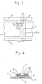
- Figures 1 and 2 show an example of a TFT fabricated by a method of the present invention.
- Figure 1 is a plan view of the TFT
- Figure 2 is a cross-sectional view of the TFT taken along a line A-A' of Figure 1.
- a gate electrode 9 branched from a gate bus line 10 and an intrinsic polysilicon thin film layer 7 (hereinafter, referred to as an "i layer") are formed on a base substrate 12 made of a glass plate or the like, sandwiching a gate insulating film 8 therebetween.
- a source electrode 2 and a drain electrode 3 are formed an the n + layers 5 and 6, respectively.
- a source auxiliary electrode la is formed on the source electrode 2 and connected to a source bus line 4. Further, the drain electrode 3 is connected to a pixel electrode 1.
- the TFT as mentioned above can be fabricated as follows:
- a metal thin film or the like is deposited on the base substrate 12 and etched into a desired configuration and size to form the gate bus line 10 and the gate electrode 9.
- the gate insulating film 8 is formed on the substrate by a CVD method or the like.
- an intrinsic polysilicon is formed on the gate insulating film 8 the i layer 7.
- polysilicon doped with n type impurities is formed on the i layer 7 as an n + layer which will be divided into the n + layers 5 and 6.
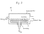
- a dry etching apparatus 20 of a parallel flat plate type in a RIE (Reactive Ion Etching) mode substrates each having the i layer and the n + layer deposited thereon in the above-mentioned manner are provided on a susceptor 21.
- an electric power having an RF electricity concentration of 0.25 w/cm 2 is applied to the susceptor 21 via an RF power supply 22.
- Polysilicons of the i layer and the n + layer react with a reaction species generated in this way to form volatile substances, and then the layers are patterned.
- the i layer has a higher activation energy than the n + layer, so that the i layer is less likely to react with the reaction species. Accordingly, it is possible to selectively etch the n + layer.
- the i layer can be patterned as a different step before or after the selective etching.
- phosphorus may be diffused and an active layer may be formed depending on the temperature at the formation of the n + layer on the i layer 7 or the thermal hysteresis in other steps.
- overetching can be used.
- the source electrode 2 and the drain electrode 3 are formed on the n + layers 5 and 6, respectively. Then, a source auxiliary electrode la is formed on the source electrode 2 and connected to the source bus 4, and the pixel electrode 1 is connected to the drain electrode 3. Further, a liquid crystal orientation film is entirely formed on the substrate and liquid crystal is sealed between the substrate and a counter substrate, thereby obtaining a liquid crystal display device.
- Figure 4 shows the results obtained by measuring the dependence of the n + /i selectivity, the uniformity of the etch rate of the n + layer (n + uniformity), the etch rates of the n + layer (n + etch rate) and the i layer (i etch rate), upon the gas pressure, in the case where the i layer and the n + layer having the activation energy of 0.2 eV are etched by using an etching gas including hydrogen chloride gas, freon-14 gas and oxygen gas with the flow ratio of 5:15:2 at a stable RF electrical density of 0.25 W/cm 2 .
- an etching gas including hydrogen chloride gas, freon-14 gas and oxygen gas with the flow ratio of 5:15:2 at a stable RF electrical density of 0.25 W/cm 2 .
- n + /i selectivity of a process is a measure of the etch rate of the layer to be etched (n + layer) relative to other material (i layer) on the wafer surface.
- the uniformity of the etch rate of the n + layer is decreased (improved) as the gas pressure raises. Further, when the gas pressure is at 53Pa (400 m Torr) or more, the etch rate of the n + layer sharply increases compared with that of the i layer. When the gas pressure is at 53Pa (400 m Torr), the n + /i selectivity becomes minimum.
- the n + /i selectivity, and the uniformity of the etch rate of the n + layer can be simultaneously improved when the gas pressure is at 53Pa (400 m Torr)or more.
- Figure 5 shows the results obtained by measuring the dependence of the n + /i selectivity, the uniformity of etch rate of the n + layer, and the etch rates of the n + layer and the i layer, upon the gas concentration of freon-14, in the case where the i layer and the n + layer having an activation energy of 0.2 eV are etched at a stable gas pressure of the etching gas of 40Pa (300 m Torr) and a stable RF electrical density of 0.25 W/cm 2 .
- the dependence are measured by varying the flow ratio X of freon-14 in an etching gas including hydrogen chloride gas, freon-14 gas, and oxygen gas with the flow ratio of 5:X:2.
- CF 4 /CF 4 +HCl+O 2 in this diagram represents the flow ratio (Viz. concentration (mol%)) of freon-14 gas against the gross volume of hydrogen chloride gas, freon-14 gas, and oxygen gas
- CF 4 /CF 4 +HCl represents the flow ratio of freon-14 gas against the gross volume of hydrogen chloride gas and freon-14 gas
- O 2 /CF 4 +HCl+O 2 represents the flow ratio of oxygen gas against the gross volume of hydrogen chloride gas, freon-14 gas, and oxygen gas, respectively.
- the uniformity of the etch rate of the n + layer is decreased (improved) as the concentration (mol%) of freon-14 gas is increased and the concentration of oxygen gas is decreased. Further, the n + /i selectivity is small when the flow ratio X of freon-14 gas is 5; and the n + /i selectivity is increased when X is more than 5 and less than 10; and the n + /i selectivity is almost stable when X is 10 or more.
- the concentration (mol%) of freon-14 gas against the gross volume of hydrogen chloride gas and freon-14 gas is 67% or more, the n + /i selectivity and the uniformity of the etch rate of the n + layer can be simultaneously improved.
- the concentration (mol%) of freon-14 gas against the gross volume of hydrogen chloride, freon-14 gas, and oxygen gas is 58% or more, the n + /i selectivity and the uniformity of the etch rate of the n + layer can be simultaneously improved.
- the concentration (mol%) of oxygen gas in the etching gas is 12% or less, the n + /i selectivity and the uniformity of the etch rate of the n + layer can be simultaneously improved.
- Figure 6 shows the dependence of n + /i selectivity, the n + uniformity, and the etch rates of the n + layer and i layer, upon the gas pressure under the same measurement conditions as those of Figure 4, except that an n + layer having an activation energy of 0.1 eV is used.
- the dependence represent the same tendencies as those of a case where the n + layer having an activation energy of 0.2 eV is used.
- the etch rate of the n + layer has a value almost twice as large as that of such a case.
- the n + /i selectivity is almost doubly improved.
- Etching is promoted in the n + layer having an activation energy of 0.1 eV because electrons of reacting molecules (radical) and those of silicon are exchanged. Accordingly, the etching is smoothly conducted and the etch rate is increased, thereby obtaining the excellent selectivity.
- Figure 7 shows the dependence of n + /i selectivity, the n + uniformity, and the etch rates of the n + layer and i layer, on the concentration (mol%) of freon-14 gas under the same measurement conditions as those of Figure 5, excepting that an n + layer having an activation energy of 0.1 eV is used.
- the dependence represent the same tendencies as those of the case where the n + layer having an activation energy of 0.2 eV is used.
- the n + /i selectivity has further improved compared with that case.
- etching characteristics can be obtained by using a polysilicon thin film having an activation energy of 0.2 eV or less for the n + layer.
- the TFT is fabricated by using the above-mentioned respective etching characteristics in the following manner:
- the i layer 7 is deposited on the substrate with a thickness a of 50nm (500 angstroms) and the n + layer having an activation energy of 0.2 eV is deposited thereon with a thickness of 50nm (500 angstroms).
- An etching gas including hydrogen chloride gas, freon-14 gas and oxygen gas having the flow ratio of 5:15:2 and a pressure of 53Pa (400 m Torr) is made to flow into the dry etching apparatus.
- the RF electrical density is set at 0.25 W/cm 2 .
- the etch rate of the n + layer is 25nm/min (250 angstroms/min) under the above-mentioned conditions.
- the n + layer should be etched for about 2 minutes.
- etching is conducted for about 3 minutes in order to remove the active layer formed in the i layer by the diffusion of phosphorus included in the n + layer, resulting in a 150% etching of an appropriate etching.
- the n + /i selectivity becomes 2, and the layers can be selectively etched.
- the i layer 7 having a thickness of 30nm (300 angstroms) is formed without remaining partially undivided on the n + layer nor being excessively etched.
- the n + layers 5 and 6 are excellent in uniformity.
- a liquid crystal display device having an excellent display characteristics can be fabricated by using the TFT formed in this manner.
- the TFT having the same structure as mentioned above is fabricated with an n + layer made of crystalline polysilicon having an activation energy of 0.1 eV.
- the etch rate becomes 50nm/min (500 angstroms/min) under the above-mentioned conditions, so that only 1 minute of etching is required to divide the n + layer into the drain region 5 and the source region 6.
- a 150% etching is conducted in order to remove the active layer formed in the i layer by the diffusion of phosphorus included in the n + layer. Under the above-mentioned conditions, the n + /i selectivity becomes 4, and the layers can be selectively etched.
- the i layer 7 having a thickness of 20nm (200 angstroms) is formed without remaining partially undivided on the n + layer nor being excessively etched. Further, the n + layers 5 and 6 are excellent in uniformity.
- the liquid crystal display device having an excellent display characteristics can be fabricated by using the TFT formed in this manner.
- a mixed gas of hydrogen chloride gas and freon-14 gas added with oxygen gas is used for the etching.
- the etching gas used for the present invention is not limited to such a mixed gas and the same effect can be obtained with a mixed gas including chlorine gas instead of hydrogen chloride gas.
- a cylindrical apparatus can be used as a dry etching apparatus for the present invention.
- modes such as a RIE (Reactive Ion Etching) mode, a PE (Plasma Etching) mode and an ECR mode can be applied for the etching mode.
- the n + layer and the i layer having an satisfactory controllability of etching and an uniform etch rate can be selectively etched by the dry etching method using an etching gas including hydrogen chloride gas and freon-14 gas free from the freon regulation.
- a TFT having an i layer of a thin film thickness can be fabricated by taking an advantage of the above-mentioned characteristics of the present invention, so that the optical pumping current can be reduced when the TFT is turned off.
- the distortion of the threshold voltage generated when the optical pumping current is introduced into a gate insulating film can be restrained, so that a liquid crystal display device having excellent display capacities can be obtained.
Landscapes
- Drying Of Semiconductors (AREA)
- Liquid Crystal (AREA)
- Thin Film Transistor (AREA)
Claims (4)
- Verfahren zum reaktiven Ionenätzen von n-Polysilicium, das auf einer eigenleitenden Polysiliciumschicht hergestellt wurde, mit einem Trockenätzen des n-Polysiliciums unter Verwendung eines Ätzgases, das durch CF4 und ein Gas gebildet ist, das aus Chlorwasserstoff und Chlor, möglicherweise mit einer Zumischung von Sauerstoff, ausgewählt ist, wobei die Konzentration von CF4 im Ätzgas die folgende ist:67 Mol% oder mehr bezogen auf CF4 und Chlorwasserstoff oder Chlor, wenn das Ätzgas aus CF4 und Chlorwasserstoff oder Chlor besteht; oder58 Mol% oder mehr bezogen auf CF4 und Chlorwasserstoff oder Chlor, wenn das Ätzgas aus CF4 und Chlorwasserstoff oder Chlor sowie Sauerstoff besteht;um dadurch das n-Polysilicium in Bezug auf das eigenleitende Polysilicium selektiv zu ätzen.
- Verfahren nach Anspruch 1, dadurch gekennzeichnet, dass der Druck des Ätzgases 53 Pa (400 mTorr) oder mehr beträgt.
- Verfahren nach Anspruch 1 oder Anspruch 2, bei dem das Ätzgas Sauerstoff mit einer Konzentration von 12 Mol% oder weniger enthält.
- Verfahren zum Herstellen eines Dünnschichttransistors mit einer Gateelektrode (9), einer einen Kanalabschnitt bildenden Halbleiterschicht, die durch einen Gateisolierfilm (8) elektrisch von der Gateelektrode getrennt ist, einem Paar Kontaktschichten (5, 6) mit Kontakt zur den Kanalabschnitt bildenden Halbleiterschicht, einer Sourceelektrode (2) mit Kontakt mit einer der Kontaktschichten (5) und einer Drainelektrode (3) mit Kontakt mit der anderen Kontaktschicht (6), mit den folgenden Schritten:Herstellen einer eigenleitenden Polysiliciumschicht (7) auf dem Gateisolierfilm (8);Herstellen einer n-Polysiliciumschicht (5, 6) auf der eigenleitenden Siliciumschicht (7) undHerstellen des Paars Kontaktschichten (5, 6) durch selektives reaktives Ionenätzen eines Teils der n-Polysiliciumschicht durch ein Verfahren gemäß einem der Ansprüche 1 bis 3.
Applications Claiming Priority (3)
| Application Number | Priority Date | Filing Date | Title |
|---|---|---|---|
| JP32102392 | 1992-11-30 | ||
| JP32102392A JP3009975B2 (ja) | 1992-11-30 | 1992-11-30 | シリコン薄膜のドライエッチング方法 |
| JP321023/92 | 1992-11-30 |
Publications (3)
| Publication Number | Publication Date |
|---|---|
| EP0600664A2 EP0600664A2 (de) | 1994-06-08 |
| EP0600664A3 EP0600664A3 (de) | 1994-11-23 |
| EP0600664B1 true EP0600664B1 (de) | 2001-05-23 |
Family
ID=18127935
Family Applications (1)
| Application Number | Title | Priority Date | Filing Date |
|---|---|---|---|
| EP93309400A Expired - Lifetime EP0600664B1 (de) | 1992-11-30 | 1993-11-25 | Trocken-Ätz-Verfahren für eine Silizium-Dünnschicht |
Country Status (4)
| Country | Link |
|---|---|
| US (2) | US5783494A (de) |
| EP (1) | EP0600664B1 (de) |
| JP (1) | JP3009975B2 (de) |
| DE (1) | DE69330241T2 (de) |
Families Citing this family (9)
| Publication number | Priority date | Publication date | Assignee | Title |
|---|---|---|---|---|
| JPH07263415A (ja) * | 1994-03-18 | 1995-10-13 | Fujitsu Ltd | 半導体装置の製造方法 |
| US6284576B1 (en) * | 1996-07-04 | 2001-09-04 | Sharp Kabushiki Kaisha | Manufacturing method of a thin-film transistor of a reverse staggered type |
| TW463300B (en) * | 1998-08-07 | 2001-11-11 | United Microelectronics Corp | Manufacturing method of self-aligned via for preventing the poisoning of the via |
| US20020177321A1 (en) | 2001-03-30 | 2002-11-28 | Li Si Yi | Plasma etching of silicon carbide |
| US7084070B1 (en) | 2001-03-30 | 2006-08-01 | Lam Research Corporation | Treatment for corrosion in substrate processing |
| FR2890236B1 (fr) * | 2005-08-30 | 2007-11-30 | Commissariat Energie Atomique | Procede de fabrication de circuits en couches minces en silicium amorphe et polycristallin |
| US9515089B1 (en) | 2015-05-14 | 2016-12-06 | International Business Machines Corporation | Bulk fin formation with vertical fin sidewall profile |
| US9627263B1 (en) | 2015-11-30 | 2017-04-18 | International Business Machines Corporation | Stop layer through ion implantation for etch stop |
| US9887135B1 (en) | 2017-04-28 | 2018-02-06 | Globalfoundries Inc. | Methods for providing variable feature widths in a self-aligned spacer-mask patterning process |
Family Cites Families (14)
| Publication number | Priority date | Publication date | Assignee | Title |
|---|---|---|---|---|
| US101302A (en) * | 1870-03-29 | Improvement in tie-bar for holding bent wood | ||
| US4383885A (en) * | 1980-02-06 | 1983-05-17 | Bell Telephone Laboratories, Incorporated | Reactive sputter etching of polysilicon utilizing a chlorine etch gas |
| UST101302I4 (en) * | 1980-03-17 | 1981-12-01 | Selective reactive ion etching of polycrystalline silicon against monocrystalline silicon | |
| JPS56144542A (en) * | 1980-03-17 | 1981-11-10 | Ibm | Method of selectively reactively ion etching polycrystalline silicon for monocrsytalline silicon |
| JPS57174466A (en) * | 1981-04-22 | 1982-10-27 | Hitachi Ltd | Dry etching method |
| US4490209B2 (en) * | 1983-12-27 | 2000-12-19 | Texas Instruments Inc | Plasma etching using hydrogen bromide addition |
| US4789426A (en) * | 1987-01-06 | 1988-12-06 | Harris Corp. | Process for performing variable selectivity polysilicon etch |
| US4799991A (en) * | 1987-11-02 | 1989-01-24 | Motorola, Inc. | Process for preferentially etching polycrystalline silicon |
| US5543646A (en) * | 1988-09-08 | 1996-08-06 | Mitsubishi Denki Kabushiki Kaisha | Field effect transistor with a shaped gate electrode |
| US4992134A (en) * | 1989-11-14 | 1991-02-12 | Advanced Micro Devices, Inc. | Dopant-independent polysilicon plasma etch |
| JPH03270223A (ja) * | 1990-03-20 | 1991-12-02 | Sharp Corp | 非晶質シリコン薄膜のドライエッチング方法 |
| JPH047822A (ja) * | 1990-04-25 | 1992-01-13 | Fuji Xerox Co Ltd | 半導体装置の製造方法 |
| EP0504390B1 (de) * | 1990-10-05 | 1996-01-10 | General Electric Company | Dünnfilmtransistorstruktur mit verbesserten source/drainkontakten |
| US5384009A (en) * | 1993-06-16 | 1995-01-24 | Applied Materials, Inc. | Plasma etching using xenon |
-
1992
- 1992-11-30 JP JP32102392A patent/JP3009975B2/ja not_active Expired - Lifetime
-
1993
- 1993-11-25 EP EP93309400A patent/EP0600664B1/de not_active Expired - Lifetime
- 1993-11-25 DE DE69330241T patent/DE69330241T2/de not_active Expired - Lifetime
-
1995
- 1995-09-07 US US08/524,886 patent/US5783494A/en not_active Expired - Lifetime
-
1998
- 1998-07-21 US US09/119,993 patent/US6133157A/en not_active Expired - Lifetime
Also Published As
| Publication number | Publication date |
|---|---|
| DE69330241T2 (de) | 2001-10-18 |
| JPH06168915A (ja) | 1994-06-14 |
| EP0600664A2 (de) | 1994-06-08 |
| US5783494A (en) | 1998-07-21 |
| DE69330241D1 (de) | 2001-06-28 |
| JP3009975B2 (ja) | 2000-02-14 |
| EP0600664A3 (de) | 1994-11-23 |
| US6133157A (en) | 2000-10-17 |
Similar Documents
| Publication | Publication Date | Title |
|---|---|---|
| US4450042A (en) | Plasma etch chemistry for anisotropic etching of silicon | |
| US7754294B2 (en) | Method of improving the uniformity of PECVD-deposited thin films | |
| KR100741435B1 (ko) | 필름 형성 전구체를 제어함으로써 실리콘 질화물 필름의 특성 및 균일성을 제어하는 방법 및 실리콘 질화물을 포함하는 tft 소자 | |
| US5286344A (en) | Process for selectively etching a layer of silicon dioxide on an underlying stop layer of silicon nitride | |
| US4789426A (en) | Process for performing variable selectivity polysilicon etch | |
| JPH0744175B2 (ja) | エッチング方法 | |
| JP3370806B2 (ja) | Mis型半導体装置の作製方法 | |
| US6686292B1 (en) | Plasma etch method for forming uniform linewidth residue free patterned composite silicon containing dielectric layer/silicon stack layer | |
| KR19980071698A (ko) | 질화 실리콘층의 에칭 방법 및 반도체 장치의 제조 방법 | |
| JPH029122A (ja) | ポリシリコンを含む層状体のエッチング方法 | |
| EP0600664B1 (de) | Trocken-Ätz-Verfahren für eine Silizium-Dünnschicht | |
| US5700699A (en) | Method for fabricating a polycrystal silicon thin film transistor | |
| US7214979B2 (en) | Selectively deposited silicon oxide layers on a silicon substrate | |
| US4479850A (en) | Method for etching integrated semiconductor circuits containing double layers consisting of polysilicon and metal silicide | |
| US6399515B1 (en) | Plasma etch method for forming patterned chlorine containing plasma etchable silicon containing layer with enhanced sidewall profile uniformity | |
| JP2000252259A (ja) | ドライエッチング方法及び半導体装置の製造方法 | |
| EP0111706B1 (de) | Seitenwandisolation der Gate-Elektrode von Feldeffekttransistoren und Verfahren zu ihrer Herstellung | |
| KR20020035747A (ko) | 보텀게이트형 박막트랜지스터와 그 제조방법 및 표시장치 | |
| JP2939783B2 (ja) | 薄膜トランジスタの製造方法 | |
| KR970003886B1 (ko) | 실리콘박막의 건식에칭방법 | |
| KR19980071537A (ko) | 도핑된 폴리실리콘층 및 폴리실리콘층 구조물의 제조 방법 및 폴리실리콘층을 포함하는 층 및 층 구조물의 구조화 방법 | |
| JPH08167597A (ja) | エッチング方法およびエッチング装置 | |
| JP2739228B2 (ja) | 半導体デバイスの製造方法 | |
| JP2692914B2 (ja) | 薄膜トランジスタの製造方法 | |
| US6191016B1 (en) | Method of patterning a layer for a gate electrode of a MOS transistor |
Legal Events
| Date | Code | Title | Description |
|---|---|---|---|
| PUAI | Public reference made under article 153(3) epc to a published international application that has entered the european phase |
Free format text: ORIGINAL CODE: 0009012 |
|
| AK | Designated contracting states |
Kind code of ref document: A2 Designated state(s): DE FR GB |
|
| PUAL | Search report despatched |
Free format text: ORIGINAL CODE: 0009013 |
|
| AK | Designated contracting states |
Kind code of ref document: A3 Designated state(s): DE FR GB |
|
| 17P | Request for examination filed |
Effective date: 19950127 |
|
| 17Q | First examination report despatched |
Effective date: 19950329 |
|
| GRAG | Despatch of communication of intention to grant |
Free format text: ORIGINAL CODE: EPIDOS AGRA |
|
| GRAG | Despatch of communication of intention to grant |
Free format text: ORIGINAL CODE: EPIDOS AGRA |
|
| GRAG | Despatch of communication of intention to grant |
Free format text: ORIGINAL CODE: EPIDOS AGRA |
|
| GRAH | Despatch of communication of intention to grant a patent |
Free format text: ORIGINAL CODE: EPIDOS IGRA |
|
| GRAG | Despatch of communication of intention to grant |
Free format text: ORIGINAL CODE: EPIDOS AGRA |
|
| GRAH | Despatch of communication of intention to grant a patent |
Free format text: ORIGINAL CODE: EPIDOS IGRA |
|
| GRAA | (expected) grant |
Free format text: ORIGINAL CODE: 0009210 |
|
| AK | Designated contracting states |
Kind code of ref document: B1 Designated state(s): DE FR GB |
|
| REF | Corresponds to: |
Ref document number: 69330241 Country of ref document: DE Date of ref document: 20010628 |
|
| ET | Fr: translation filed | ||
| REG | Reference to a national code |
Ref country code: GB Ref legal event code: IF02 |
|
| PLBE | No opposition filed within time limit |
Free format text: ORIGINAL CODE: 0009261 |
|
| 26N | No opposition filed | ||
| PGFP | Annual fee paid to national office [announced via postgrant information from national office to epo] |
Ref country code: DE Payment date: 20121121 Year of fee payment: 20 Ref country code: FR Payment date: 20121130 Year of fee payment: 20 |
|
| PGFP | Annual fee paid to national office [announced via postgrant information from national office to epo] |
Ref country code: GB Payment date: 20121121 Year of fee payment: 20 |
|
| REG | Reference to a national code |
Ref country code: DE Ref legal event code: R071 Ref document number: 69330241 Country of ref document: DE |
|
| REG | Reference to a national code |
Ref country code: GB Ref legal event code: PE20 Expiry date: 20131124 |
|
| PG25 | Lapsed in a contracting state [announced via postgrant information from national office to epo] |
Ref country code: GB Free format text: LAPSE BECAUSE OF EXPIRATION OF PROTECTION Effective date: 20131124 Ref country code: DE Free format text: LAPSE BECAUSE OF EXPIRATION OF PROTECTION Effective date: 20131126 |